Alma Mater Studiorum · Universit`
a di Bologna
Scuola di Scienze
Corso di Laurea Magistrale in Fisica
Programmable Electronic Platform for the
remote control of the Cell-Migration
Galvanotaxis
Relatore:
Dott. Alessandro Gabrielli
Correlatore:
Dott.ssa Isabella Zironi
Presentata da:
Luca Boccioletti
Sessione III
“Per Aspera ad Astra” A chi non smette di sognare
Abstract
Il presente lavoro di tesi nasce come collaborazione tra il Laboratorio di Progettazione Elettronica e il Laboratorio di Microscopia a Fluorescenza del Dipartimento di Fisica e Astronomia dell’ Universit`a di Bologna. In particolare nasce dalla volont`a di dotare il dipartimento di un apparato sperimentale in grado di svolgere studi sulla Galvanotassia, un fenomeno biologico consistente nella migrazione di cellule sottoposte a stimolazione elettrica. La Galvanotassia `e nota da fine ’800 ma non sono ancora chiari i meccanismi cellulari che la provocano. Una migliore comprensione di tale fenomeno potrebbe portare importanti sviluppi in ambito medico, sia diagnostici che terapeutici. Dalla letteratura a riguardo non `e emersa l’ esistenza di apparecchi elettronici di controllo che permettano lo studio della Galvanotassia e che possano essere duttili a seconda del tipo di esperimento che si voglia svolgere. Da qui l’ idea di iniziare lo sviluppo di un dispositivo elettronico, che fosse riprogrammabile, a basso costo e facilmente trasportabile. La progettazione di questo dispositivo ha portato ad una prima fase di test e verifiche sperimentali che hanno permesso di migliorare e affinare la costruzione di uno strumento di misura e controllo dei parametri relativi alla Galvanotassia. Sono gi`a stati programmati test futuri che porteranno ad una versione definitiva dell’ apparecchiatura alla quale succederanno pi`u approfondite ricerche sul fenomeno della Galvanotassia.
Abstract
The present work is born as a collaboration between the Laboratory of Electronics Design and the Laboratory of Fluorescence Microscopy of the Department of Physics and Astronomy of the University of Bologna. In particular it arose from the desire to equip the department of an experimental apparatus able to perform studies on Galvanotaxis, a biological phenomenon consisting in the migration of cells when subjected to electrical stimulation. The Galvanotaxis is known from the end of ’800 but are not yet clear the cellular mechanisms that cause it. A better understanding of this phenomenon could lead to important developments in medicine, both diagnostic and therapeutic. From the literature on this subject it has not emerged the existence of devices that allow the study of the phenomenon that may be adaptable depending on the type of experiment that you want to play. From here the idea of starting the development of an electronic device, which was re-programmable, low-cost and easily transportable. The design of this device has led to a first phase of tests and experimental verifications that have allowed to improve and refine the construction of a measuring and control instrument of the parameters related to Galvanotaxis. They have already programmed future tests that will lead to a final version of the device which will be followed by further research on the phenomenon of Galvanotaxis.
Contents
Abstract III
Abstract V
Introduction 1
1 Galvanotaxis and Biological Experimental Setup 3
1.1 Galvanotaxis . . . 3
1.2 Data Acquisition System . . . 6
1.2.1 Nikon Eclipse Ti . . . 7
1.2.2 Incubator . . . 8
1.2.3 Nis-Elements software . . . 9
1.3 T98G Cell Line . . . 9
2 Design and Development 11 2.1 Arduino Due . . . 11
2.2 Support plate for incubator . . . 13
2.3 Electronic platform for the remote control of the cell-migration Galvanotaxis 15 2.3.1 Design . . . 15 2.3.2 Construction . . . 16 2.4 Sketch . . . 20 3 Measurements 25 3.1 Voltage Measures . . . 25 3.2 Measures of Currents . . . 29 Conclusions 35 Appendix 46 VII
Aknowledgements 47
Introduction
The Galvanotaxis is a biological phenomenon already known from the late nineteenth century that states that certain motile cells, when subjected to electric type stimuli tend to migrate all in the same direction. This phenomenon has been observed in many biological processes of medical interest but to date the cellular mechanisms that cause it are not yet fully known. This thesis was born as collaboration between the Electronic Design Laboratory and the Fluorescence Microscopy Laboratory of the Department of Physics and Astronomy of University of Bologna. Given that in the literature have been found several sources that spoke of different types of stimuli both in intensity and in time; the intention was to start a search that would lead to obtain a device for the electrical stimulation of the cells that were low-cost, re-programmable, remotely controllable and easily transportable.
After an initial phase of the study of the problem, the commercial Arduino board has been chosen as the main electronic apparatus to start designing the entire electronic remote control of the biological cells. For this reason it was designed and attached a contour circuitry and a firmware that was functional to the requirements. The entire electronic device, once assembled, has been tested in the laboratory and some preliminary measurements were performed. The measures carried out have led to some changes in the electronic platform and to a better understanding of the problems related to the development of a galvanotactic chamber. This study has also resulted in the development, thanks to the collaboration of the mechanical facility of Istituto Nazionale di Fisica Nucleare (INFN), of a support board for the cell culture that was integrated into an incubator for in vivo measures and that could contain any electronics required without damaging the cell culture. The measurements were performed by stimulating the cells with external electric fields and electric currents.
The first chapter introduces the phenomenon of Galvanotaxis, briefly explaining some theories about it, shows the experimental setup used to perform biological experiments and the cell line used. The second chapter is about the peculiarity of the Arduino board, the design and the development of Programmable Electronic Platform and explains one of the possible firmware versions that permits to use it. In the third chapter the tests performed, the results and the future developments will be shown.
Chapter 1
Galvanotaxis and Biological
Experimental Setup
This chapter briefly explains the phenomenon of Galvanotaxis, the data acquisition system, which it is composed of an optical microscope capable to performs in vivo mea-surements thanks to an incubator placed on its stage and the type of cells that have been used in this work.
1.1
Galvanotaxis
Galvanotaxis (also known as Electrotaxis) is a word that indicates the movement of a living organism in response to an electrical stimulus. This word owes its name to the Italian physicist and physician Luigi Galvani, who was the first scientist to perform studies of bioelectricity in the eighteenth century along but independently from the physician Alessandro Volta. In particular, the term Galvanotaxis, in biology means the movement of a cell subjected to currents induced by a continuous electric field (dcEF). The first studies in this field date back to the end of the nineteenth century thanks to Ludloff(1895) and Verworn(1899)[1] and they were conducted on unicellular organisms.
Endogenous electric fields are normally present in nature in the magnitude of mVmm−1[2] and it has been shown that these have an important role in physiological processes of medical interest such as: embryogenesis, angiogenesis, wound healing and metastasis. The experiments conducted have shown that some types of cells, when subjected to dcEFs of the same magnitude as those endogenous, tend to orientate and to migrate along the axes of the electrical potential. Depending on the cell type it is seen as they move in a selective manner to the cathode or to the anode, even though most of the work done has shown mainly a migration toward the cathodical side of the field. To
Figure 1.1: Portraits of Luigi Galvani (on the left) and Alessandro Volta (on the right).
date, the actual mechanism behind the Galvanotaxis remains unclear although several theories have been proposed about.
The electrical properties of the cell are mainly due to the cell membrane[3]. In fact outside of the membrane cells are soaked in a conductive medium, but thanks to the high resistance of this, with respect to the external medium, much of the current flow created by the electric field passes out of the cell, without creating effect on the internal structures. Not only in the media but even in the Cytoplasm the ions are present. So the cell will tend to undergo a polarization when subjected to an electrical stimulus (fig 1.2).[4]
Figure 1.2: Polarization of ions inside the cell in the presence of an external electric field. (Przemyslaw B. 2012)
The membrane, however, is provided with structures called ion channels that are able to create, also in a selective manner, an electro-osmotic flow of ions. Just these channels,
1.1 Galvanotaxis 5
in particular the Voltage Gated Calcium Channels (VGCCs), so even the concentration of Ca2+ seem to be apparently responsible for the galvanotactic response, response that
might operate in the short term (seconds/minutes) and the long term (minutes/hours). It is believed that the opening of this channels, from the anodic side, hyperpolarised the cell thereby creating a so-called calcium wave (fig. 1.3) that would create a structural deformation of the cytoskeleton such as to allow a migration towards the cathode. It is seen as inhibiting these channels or reducing the concentrations of Ca2+ ions in the
medium, the galvanotactic effect appreciably decreases. But recent studies have high-lighted as also the concentration of Na+ ions and consequently the activity of Voltage Gated Sodium Channels (VGSCs) may have a role in the phenomenon.[5] The majority of the cells showed sensitivity to electrical stimuli and the few that have not shown are those that already normally have low motility. The galvanotactic response is independent to that chemotactic.
Figure 1.3: A cell exposed to a dcEF. The membrane towards the anode is hyperpolarized and attracts Ca2+. Consequently, this side of the cell contracts, thereby propelling the cell towards the cathode. (Mycielska M.E. and Djamgoz M. B. A. 2004)
The design of the galvanotactic chamber isn’t sensibly changed through the years. Typically they use agar salt bridges for conveying the electric current inside the media of cell culture. Two are the methods used mainly. The first one is the creation of a “channel” inside the Petri dish to convey the electric current in the middle[6] (fig.1.4). The second one is to use a microfluidic chamber[7] in order to obtain a best shaping of the dcEF. The second method is simpler but it does not allow the study on cell population but only on single cells. New articles have also highlighted as monolayers of cells have a galvanotactic behaviour and field inversions, even too short (minutes), are visible creating real motion reversals such as U-turns.
the reasons mentioned above it is deduced as the real understanding of this phenomenon, known but not entirely clarified, can lead to the development of new diagnostic or medical techniques of considerable interest.
Figure 1.4: Scheme of a typical galvanotactic chamber. (Zhao M. et al. 2006)
1.2
Data Acquisition System
The laboratory of fluorescence microscopy of the Department of Physics of the Uni-versity of Bologna is equipped with an inverted optical microscope. In particular a Nikon Eclipse Ti integrate with a live cell chamber. This data acquisition system is able to perform in-vivo measurements.
1.2 Data Acquisition System 7
1.2.1
Nikon Eclipse Ti
The Nikon Eclipse Ti is an inverted optical microscope, associated with software Nis-Elements 3.1, that is capable to acquire different kinds of images: bright-field, contrast-phase, fluorescence. It is called inverted because it has its light source on top pointing down, while the objectives are under the stage pointing up. In this work we have used the contrast-phase microscopy technique, acquiring images in time-lapse thanks to the integrated incubator.
The contrast-phase microscopy is a technique that allows to point out the different components of a cell. Not normally visible with the standard technique (bright-field). This technique converts little phase shifts of the light in changes of amplitude that will be visualized on the image as a gray levels. The phase shifts are due to the different refractive index of the specimen components. If the refractive index of the crossed component is greater than the medium the speed of light will be lower and the delay of this wave will be greater than the others that have crossed only the medium.
Below are the main components of the specific instrument used: Source of light: the light source is an HBO mercury-vapor lamp.
Shutter: the Smart Shutter LAMBDA SC is a diaphragm, automatic programmable and controlled by software, that permits to alternate different phases of illumination of the sample. This mechanism allows to avoid switching on and off of the lamp.
Figure 1.6: Image of the objectives mounted on the microscope.
Objectives: this type of microscope has a variety of different objectives. This arrangement is intended to ensure that it can be used exploiting the various previously mentioned techniques of microscopy. For example for the dynamic imaging it is necessary to use an objective with a high signal transfer efficiency.
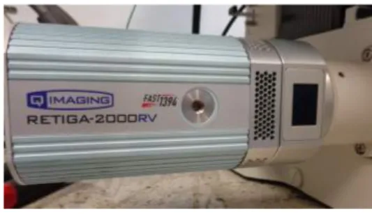
Camera: The RETIGA 2000 RV is a digital camera based on a CCD detector, designed to aquire low intensity signals. It has an integrated cooling system that it allows to adjust the temperature to −30oC. It is also synchronized with the other system
Figure 1.7: RETIGA 2000 RV digital image camera.
components. The CCD detector is 1.92 Megapixel large, with a 12 bits output (4096 gray levels) and the exposure time can change from seconds up to minutes. PFS: the Perfect Focus System is a hardware solution invented by Nykon in order to
avoid the loss of focus extremely useful especially during time-lapse acquisitions.
1.2.2
Incubator
Figure 1.8: The incubator on the microscope stage. The tubes which are seen are those for monitoring environmental conditions.
It is produced by Oko-Lab and is designed to maintain all the environmental con-ditions for cell cultures. It is basically formed by a case where temperature, humidity and CO2 concentration are constantly monitored and modified. The temperature is
ad-justed by a thermal bath thermostat and monitored by a thermocouple. A compressed air pump coupled with a CO2 cylinder are linked to the same control system and allow
1.3 T98G Cell Line 9
the right humidity the thermal bath is capable to produce steam and to pump it inside the incubator.
1.2.3
Nis-Elements software
Provided by Nikon, this software is used to control the microscope. It is able of managing all of the instrument parameters as: time of exposition and aquistition mode. It is also capable to modify and analyze images previously acquired thanks to the digital image analysis tools in it of which is provided.
1.3
T98G Cell Line
T98G is a cell line derived from a human glioblastoma multiforme tumor (GMB). This is the most aggressive invasive and malignant brain cancer. These cells are immortalized, they can proliferate indefinitely.
Figure 1.9: Histological image of a Glioblastoma
After diagnosis lifespan is around 12-15 months with a mortality rate of 95-97%. The glioblastoma is so named because it emerges from the glial cells, cells that provide support for the central and peripheral nervous system. Especially it emerges from the astrocytes, star-shaped cells. It is also called grade IV astrocytoma. GMB is found mainly in the brain but can also be found in the spinal cord. T98G are cells arrested in G1 phase
under stationary phase conditions. Similar to fibroblast, they have shown good adhesion properties, high invasiveness and great movement capability “in vitro”. They exhibit numerous alterations in genes that encode for ion channels. It was hypothesized that these type of alterations could facilitate the passage of ions through the cell membrane, making them more sensitive to telectrical stimuli, Galvanotaxis including.
In the tests performed in this work, the T98G cells were cultured in RPMI 1640 media with 10 vol.% bovin serum (FBS), 1 vol.% L-glutamine, Sodium pyruvate (0.01M) and antibiotics such as penicillin (100 U/ml) and streptomycin (µg/ml). The cells are kept in the incubator under optimum culture conditions: 37oC, 100% humidity, 5% CO2
concentration.
Chapter 2
Design and Development
This chapter is the main chapter of this work. Here we will explain the characteristics of the Arduino Due board and the design and the development of the platform for the electronic control of the Galvanotaxis chamber. Also part of this work was to design a plate that was integrated in the incubator and could accommodate the necessary components.
2.1
Arduino Due
The Arduino is an open-source microcontroller board. The Arduino project has been developed to give the possibility to building simple, low cost and programmable digital devices capable to interact with the real world. The board is composed of a microcon-troller with electronic complementary components. These devices are programmable and the Arduino project provides the Arduino integrated development environment (IDE). A firmware written with this specific IDE is called a “sketch”. In particular, it has chosen to use an Arduino Due board, produced by the Italian Arduino S.r.l., because it has two DAC (Digital-to-Analog) converters, useful to generate analog signals. The Arduino Due board is based on the Atmel SAM3X8E ARM Cortex-M3 CPU. The core is a 32-bit ARM microcontroller with a CPU clock at 84MHz. Unlikely other Arduino boards, the maximum operating voltage that the I/O pins can tolerate is 3.3V. The board can be interfaced with a a PC via USB cable. The USB port is used to program the microcon-troller or even to feed it. It’s possible to use an external power supply such as a battery or an AC-to-DC adapter. The board can operate on an external supply of 6 to 20 volts. Some technical specifications of the board can be seen in the tab. 2.1. For more details refer to the official data sheets.
In the recent articles about Galvanotaxis it arose as the cells are sensitive even to sinusoidally oscillating field with a period of magnitude of minutes. So the eventuality
Figure 2.1: An Arduino Due board
of stimulating the cells with this kind of inputs has obviously led to choose a board that allows the modulations of analog output signals instead of using the Pulse-Width-Modulation (PWM). A DAC indeed is a device that converts digital data into an analog signal. With some electronic components it was possible to build a 2-output channels waveform generator. In particular the DACs of the Arduino Due board do not have an analog output voltage from 0V to Vref, that was previously set to be 3.3, but it goes from
1/6 to 5/6 of the reference. So the minimum voltage is Vmin = 0.55V and the maximum
is Vmax = 2.75V. These data, found on the datasheet, are tested experimentally and
confirmed. So the output voltage range of the DAC is equal to 2.2V. Having the device a 12-bit resolution we can also state that the DAC has resolution of 0.537mV. Eventually this problem can be avoided by constructing a simple differential amplifier realized with an op-amp. This would eliminate the voltage offset and allow to amplify the output signal.
2.2 Support plate for incubator 13
Microcontroller AT91SAM3X8E Operating Voltage 3.3V
Digital I/O Pins 54(12 PWM) Analog Outputs Pins 2(DAC) Flash Memory 51 kB SRAM 96 kB Clock Speed 84 MHz Length 101.52 mm Width 53.3 mm Weight 36 g
Table 2.1: Some technical specifications of the Arduino Due board.
2.2
Support plate for incubator
To perform the measurements was also necessary to develop a support for the petri dish that could be integrated in the incubator and that would allow to maintain the environmental conditions suitable for the survival of the cells.
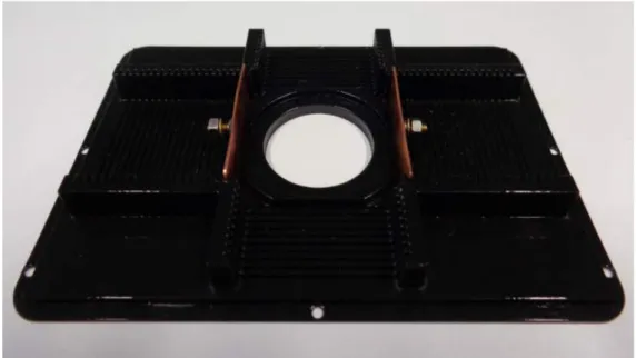
Thanks to the mechanical department of the INFN (Istituto Nazionale di Fisica Nucleare) we were able to create the support. The first prototype has been realized by using a prototype maker machine. This tool is capable, given a project file, to realize high precision models of plastic resin.
As seen in fig. 2.2 the board was developed to have the petri dish in the middle. The dimensions of the support are of 135×95 mm. It has also been studied not only for hous-ing the cell sample and any other components of the system that can be accommodated in the incubator but also with the ability to mount from one to four rectangular con-ducting metal plates of the dimensions of 40×12 mm. This solution has been designed in order to obtain dcEFs, even multipartite, to study also the application of external fields. In particular the conducting plates are made of copper. The nut and the washer are for connection of the plates, via wires, to the external electronic platform. The various visible notches serve to vary the distance between the plates. The distance between two consecutive notches is of 2mm. This is used to achieve different strength of dcEFs and to control them. In fact, known the formula:
E = V d
where E is the electric field, V is the voltage and d is the distance between the plates, we can easily calculate the theoretical strength of the field. The minimum distance reachable
Figure 2.2: The first prototype of support for petri dish made of plastice resin. The dimensions are of 135×95 mm
between the two plates is of 42.5mm. So, for example, if we have V = 1V we obtain E =24 mVmm−1. It can be seen as the area reserved for the sample is not exactly at the same height of the plates but a little bit higher. This arrangement serves to ensure that the growing medium, considerable at the same height of the base of the petri, is in the center of the electric field that will be created. In fact, thanks to this, we can consider, ignoring edge effects, that the center of the culture medium will be subjected to a uniform electric field. The holes on the outer part of the subject, which are seen in the figure, serve to ensure the support at the base of the incubator. This, in fact, will be the real bottom of the container in order to avoid heat or humidity loss.
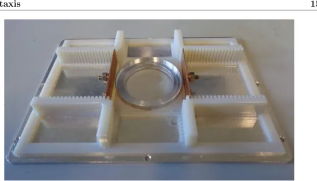
The first temperature leak tests led to consider the usefulness of building a support made of material that scatter less heat. So we decided to develop a second prototype, exactly equal to the previous one, but with the metal base and with the use of plastics components only for the guides of the conducting plates (fig. 2.3). This base is the same size as the plastic one. Even the conducting plates and spacing between theme are the same.
Preliminary tests conducted later showed how this choice was better than the previous one.
2.3 Electronic platform for the remote control of the cell-migration
Galvanotaxis 15
Figure 2.3: The second prototype of support for petri dish made of metal. Dimensions 135×95 mm
2.3
Electronic platform for the remote control of the
cell-migration Galvanotaxis
Below the steps that led to the design first and then to the realization of the electronic platform will be explained.
2.3.1
Design
The idea was to design a circuit that allows the the individual digital control of five different outputs and the possibility to control one of them with an analog output from the waveform generator.
In order to design and study the components and to testing the sketch we used, in addition to the Arduino Due board, a breadboard. This is a construction base for prototyping electronics. On a breadboard, it is not necessary to solder the electronic components. So it is reusable, cheap and excellent for prototyping.
The prototype circuit is shown in figure 2.4. The five LEDs had to simulate the five outputs. Not knowing exactly the LEDs that were available it was decided after a series of tests that the optimal solution was to use to the anode side five 47 ohm resistors. All the resistors used in this work are precision resistors with five bands. The LEDs are used to have a visual and immediate evaluation of the operation of the circuit.
(a) (b)
Figure 2.4: Representation of the prototype circuit (a) and circuit diagram (b).
The main switch of the circuit is the toggle switch S3. This switch allows you to decide which mode to use the circuit: digital or analog(DAC). The central position is the idle position. In analog mode we can decide whether to use the LEDs 1 and 4 or the LEDs 2, 3 and 5 at the same time. This capability is given by the button S5. The components in the red box are the components of the waveform generator. The two switches are used to change the waveform output from the two converters while the potentiometer, thanks to the reading of its signal, is used to vary the frequency. A better understanding of its operation is postponed to the paragraph on the sketch. The switch in the blue box is used only to control the LED1 and to avoid the voltage input into the pin declared as digital voltage output.
As shown in fig. 2.5 the two DACs really generate a waveform signal, visible on the screen of a oscilloscope. With the sketch explained below the two DACs are capable to generate four different waveform: sinusoidal, square, triangle and sawtooth.
2.3.2
Construction
The platform was build on a stripboard. The stripboard is a plastic board with a regular grid of holes. In the lower part of the board there are copper strips that connect all the holes on the greater side (fig. 2.6). This choice has been made to make
2.3 Electronic platform for the remote control of the cell-migration
Galvanotaxis 17
Figure 2.5: Testing the wave generator.
the circuit permanent. In fact, the electronic components have been soldered on the stripboard. The board has the dimensions of 160×100 mm. The holes are arranged in 38 rows by 61 columns, spaced with standard pitch equal to 2.54mm, for a total of 2,318 holes. The two upper strips of the board have been used for the 3.3V (Vref) and for the
ground. The choice of using 3.3V was made according to the technical specifications of the Arduino due board. Higher voltages, if sent back inside the microcontroller, would cause the destruction of the input pin. Every component of the platform is not directly and permanently connected with the Arduino Due board. This arrangement coupled with the possibility of reprogramming the Arduino allows to have a choice of different configurations virtually infinite. The device was mounted inside a sealable plastic box to be more easily transportable and avoid accidental breakage. The case and then the complete device have the size of 200×119×30 mm. Given the size of the device it is easily transportable to be repaired or possibly reprogrammed while away from the acquisition systems.
The type and number of components of the platform can be found in tab. 2.2. Each resistor used is of the E96 series so it has tolerance equal to 1%. The 5kΩ resistors were used for the switch and the three buttons. All of them are in pull-down config-uration. This expedient has been used to make sure that when the specific terminal is disconnected, the value read by Arduino is really a logical low state. For each elec-tronic component soldered on stripboard it has been mounted at least one pin (two for the switch). Consequently each of them can be connected with the board, through the jumper wires.
This arrangement is meant to have a switch that works as the mode dial, the central position can be used for the idle. In this specific case it is used to select the digital or the analog mode. The pusbutton below is used as another mode dial. For example we
Figure 2.6: A typical stripboard.
Figure 2.7: The programmable electronic platform soldered an mounted inside the plastic case.
can program the board in such a way that the pressure of the button will enable certain outputs rather than others. The screw terminals and the LEDs indicated by the arrow and inside the black box (fig. 2.7) were conceived as eight digital outputs. The right side of the stripboard (the part indicated by the white arrows) should be the wavegenerator.
2.3 Electronic platform for the remote control of the cell-migration
Galvanotaxis 19
As said earlier, the two pushbuttons are the waveform selector and the potentiometer serves a frequency selector. The two screw terminals are, if properly connected, the two outputs from the DAC. The circuit diagram of one of the possible configuration can be seen in fig. 2.8 (a larger image can be found in the Appendix). This is the configuration that has been programmed with the sketch written in this work.
Components Number Screw Terminals 8 LEDs 8 Switch 1 Pushbuttons 3 47Ω Resistors 8 10kΩ Resitors 5 10kΩ Potentiometers 1
Table 2.2: Type and number of components of the platform.
After the first tests carried out on the platform emerged the concern that it could be necessary to also have an output that could regulate a possible current flow out. This, given the possibility, not only to feed conductive plates for generating an external electric field but also for that of placing two electrodes in contact with the cell culture medium in order to generate a current flow inside the petri dish. The solution has been found adding a new output to the platform. This new line, that terminates with a screw terminal, it has been build by putting a 1kΩ and a 1MΩ potentiometer in series. To monitor the electric current that flows in the line, two pins were been mounted one before and one after the resistor. These were thought to be connected to a voltmeter. The reading of the voltage drop, known the voltage at the heads of circuit and the resistance, thanks to the Ohm’s law allow to calculate the electric current that flows.
The components are mounted on the right side of stripboard. From figure 2.9a you can understand how they were assembled and in what exact position. The circuit diagram associate (fig.2.9b) permits to easy theoretically calculate the current range available (from minimum to maximum of the potentiometer). When the potentiometer is at its maximum value, we can neglect the other resistor in series. So:
if R2min = 0Ω ⇒ Imax = 5mA
if R2max = 1M Ω ⇒ Imin = 5µA
Then, in the case of voltage equal to 5V and in this configuration the current range goes from 5µA to 5mA. The calculations are confirmed by the reading of the values on the
Figure 2.8: The circuit diagram of one of the possible configurations of the support. Specifically, that which has been designed and programmed in this work.
voltmeter. In fact, as you would expect, given that reading is done on R1, the maximum value read is equal to 5V and the minimum to 5mV. The two pins for the voltmeter were been mounted not only to control and regulate the current but also, given that the resistance of the cell culture media is unknown, to measured it and eventually to collect its variation during the experiment.
2.4
Sketch
The firmware, called sketch beacause it has been written in the specific IDE for Arduino, was been designed to control the setup configuration in fig. 2.8. As explained before this sketch allows two use the electronic platform in two modes, digital and analog using a switch. In digital mode we can turn on and off the six digital output pushing a
2.4 Sketch 21
(a)
(b)
Figure 2.9: Image of the assembly of components for controlling the current (a) and as-sociated circuit diagram (b) in the case that the output is short-circuited on the Arduino due board.
button. In analog mode we use two DAC to create different waveform, changing them with a button e selecting the frequency turning a knob. The entire code can be found in Appendix. As every sketch is composed of two main void function: setup and loop. These two functions must always be present in every sketch, even the most simple. The setup function is used to initialize the I/O pins and to define other settings. The loop function is the main part of a sketch, has repeatedly invoked, contains the instructions that permit to microcontroller to interface itself with the external environment. The execution of this function is stopped only with the shutdown of the board. Here we will explain the main parts of the code and the functioning of the waveform generator.
First of all some variables were declared and initialized with statement as:
int i = 0;
int configu = LOW;
//INPUT
int swt1_1 = 22;
//OUTPUT
the variable “i” has been declared as integer ad initialize, the variable “configu” has been initialized as logic state LOW. In fact the Arduino IDE gives the possibility to initialize the variables, not only as numbers but also as logic state. The other two statements are examples of variables used as variable for the pins of Arduino. The numbers is not a numeric value but the number that idfentifies the pin on the board. So the statement declares that the variable “LED!1” is integer and it refers to the pins number 13. An example of what can be found in the function setup is:
void setup() {
analogWriteResolution(12); // analog output resolution to 12 bit analogReadResolution(12); // analog input resolution to 12 bit
pinMode(22, INPUT);
pinMode(13, OUTPUT); }
As already said before, the function has the task to define the settings of the board. In fact the lines of code above declare that the reading and writing resolution of the board will be of 12 bits. Normally, by default, the resolution is of 8 bits. This shrewdness is necessary in order to use the 12 bits DAC available. The third and the fourth lines declares in which mode the pins have to be used. Normally all the digital pins of Arduino are I/O pins. Only after these statements they become input or output ports. Another important line of code is:
attachInterrupt(button0, wave0Select, RISING);
This is used to control the buttons that change waveform. It means that the function “wave0select” will be executed only when the pin linked to the variable “button0” sees a rising edge. The variables “swt1 1” and “swt1 2” are the variables for the selection mode switch. Their values, read by the function “digitalRead”, compose the couple of value that checked by the control structure “if” decide the mode. The exact line of code is:
if (val1_1 == LOW && val1_2 == LOW) {instructions to execute}
In this specific case it has been reported the line of code for the idle mode. It is obviously to understand that when the variable are in the logic low state at the same time, the switch is in the middle position. To avoid strange behaviours of the platform it has
2.4 Sketch 23
been written the same code for the case in which both variables are in the logic high state. The lines of code that follow the control structure recall the functions that write a specific state at the output. For example:
digitalWrite(LED1, LOW);
analogWrite(DAC0, 0);
the function “digitalWrite” will write on the output pin declared as LED1 the logic low state and “analogWrite” will write on the output of DAC0 the minimum value available (DAC off). Inside the block of code on digital mode, there is another control structure “if” that, after pressing the button near the switch, enables or disables the digital outputs (from low to high or viceversa) and the related LEDs. In this specific sketch all the digital outputs and the LEDs are simultaneously at the same logic state.
The analog mode, enabling the waveform generator, is based on the line: analogWrite(DAC0, Table[wave0][i]);
this function turn on the DAC and read an array of indexed value written in an header file (see the appendix for the entire header file) that is recalled at the beginning of the firmware. Inside the header file there are: two definitions and four arrays. The definitions declare the number of waveform contained in it and the maximum number of values for each of them that it is equal to 120. The values are written in hexadecimal form and goes from 0 to 4095. Every time that the the line above is invoked one of the value is taken and sent to the DAC that converts it in an voltage output included between 0.55V and 2.75V. Every loop, the index “i” is increased by one so scrolling the list of values. The frequency of the wave is controlled by the potentiometer. Turning it we can change the period. This setup allows to go from a minimum frequency of 1Hz to a maximum of 170Hz. Tho do this it was necessary to define the so called “oneHzSample” as
1000000µs
maximumnumberof values =
1000000µs
120 = 8333µs
this is the time that, called with the function “delay”, stop the loop every time that a sample value is taken. It easy to understand that to complete an entire waveform, in this case, we have to complete 120 loop for a total time of 1s that it is exactly the period of the wave of frequency equal to 1Hz. The minimum frequency, when the potentiometer, is set to zero, is due to the intrinsic delay of the microcontroller. The value is given by the constructor. So with an easy calculus we can obtain, maximum frequency known, the minimum sample rate. If we call the period T :
T = 1
170Hz = 5882µs ⇒ min sample rate = 49µs
sample = map(analogRead(A7), 0, 4095, 0, oneHzSample);
This line maps the voltage signal, that can go from 0V to 3.3V, in a value included between 0 and 4095 (12 bits) and then remaps it in a value that goes from zero to the maximum sampling rate. Every time that the entire list of value has been read the firmware from the beginning of the list because the index “i” is set to zero. It is the same for the choice of the waveform, that they has been read every time in the same sequence. The frequency range can be changed, for example, by adding the same number of values in the header file. Different waveforms can be created, theoretically infinite, creating the right list of values.
So with this sketch and this configuration the platform has the characteristics shown in tab. 2.3. Digital mode number of outputs 6 LOW 0V HIGH 3.3V Analog mode number of outputs 2 number of waveforms 4 min freq. 1Hz max freq. 170Hz
Table 2.3: Some details of the electronic platform with the configuration and the sketch ecplained.
Chapter 3
Measurements
In this chapter we will explain the types of measurements performed with the use of the programmable electronic platform and the support plate for the petri dish. It will be explained the setup used and observations made. The tests made are of two types. In the first one an external electric field was used to stimulate the cell. In the second one it has created an electric current through the cellular culture medium.
3.1
Voltage Measures
The first measurements were designed to see if a dcEF (direct current electric field) could create a Galvanotaxis phenomenon or whether the cells will move all in the same direction. To achieve this was used the support plate with inserted two copper conductive plates. The distance used was the minimum obtainable, that is equal to 42,5mm. The measurements were always done in the same way. First, the support was placed in the incubator and the cables have been connected to the voltage external generator (as shown in fig. 3.1). Then the incubator was closed and brought to the optimum temperature of 37o and the optimal environmental conditions have been reached. At this point it
has been inserted on the plate the petri dish containing the cell culture. It was then searched the best observation point by pointing the microscope using a 20× objective. The total acquisition lasted two hours by recording with an acquisition rate of one frame per minute. The first hour was not turned on the field, this in order to acquire what is called the “base line” or an observation of the cell culture without stimulation. At the beginning of the second hour the voltage was given to the copper conductive plate. A total of 120 images were acquired, 60 with field and 60 without.
In the first experiment we used a tension equal to 5V, applied for 1 hour, using the specific output of the Arduino base. So theoretically we got a field at the center of the
Figure 3.1: The conductive plates of the support plate linked to the electronic platform.
capacitor equal to:
5V → E ∼= 118mV mm−1
In these conditions, analyzing the acquired images (fig. 3.2), we did not see any significant shift of the specimen. We thought that the problem could be a too low voltage applied. So we decided to increase it.
For the second test, thinking that the problem was a too low voltage, the plates were connected to a voltage generator model CPX200 manufactured by Aim TTi (3.3), able reach up to 35V. The experiment took place under exactly the same conditions as the previous one, so 37oC and controlled environmental parameters. This time we decided to
use a voltage equal to 20V. Again we can calculate the theoretical strenght of the field: 20V → E ∼= 470mV mm−1
3.1 Voltage Measures 27
(a)
(b)
Figure 3.2: The last frame of the base line (a) and the last one after one hour of dcEF (b). No movement in a certain direction can be seen.
Even in this case we did no note any significant shift of the specimen. On of hypoth-esized idea could be that the range of voltages used is inappropriate. Another idea that
Figure 3.3: A voltage generator model CPX200.
could be reasonable is that the phenomenon that we are trying to achieve could have a threshold. So if we do not use the exact voltages, maybe higher, the cellular shift will not start. However, these experiments have led us to consider the possibility of use current instead of voltage to stimulate the cells. The changes to the setup and the test carried out are explained in the next section.
3.2 Measures of Currents 29
3.2
Measures of Currents
The second type of test performed was based on the circulation of electric current within the cell culture medium. To perform this we had to modify the electronic platform and the support plate. To the platform were added: 1kΩ resistor, 1MΩ potentiometer and a screw terminal to wire the line to the platform (explained in the previous chapter). The setup has been designed in such a way that the contacts, thanks two electrodes, of the culture medium allowed the flow of an electrical current. As electrodes we decided to use two Ag/AgCl wire. This type of electrodes are commonly used in biological applications. For example act as reference electrode in patch clamp experiments. They also have the advantage that the only species involved in the electrochemical reaction that you are going to have on the electrode surface is the generation or consumption of chloride ions avoiding other kind of reactions. These electrode do not have to contact directly the culture medium, in order to do not alter the right living conditions of the cells. So we decided to use the agar gel as a salt bridge. To achieve this configuration we used two pipette tips previously bent to be positioned on the platform. These were filled with agar gel, and then the electrodes were inserted in them. The entire device thus constructed was then placed in the incubator, as shown in fig. 3.4(a). To contact the electrodes with the cables, we used the specific connectors that have been prepared before (fig. 3.4). In this case we have a 100× objective and the acquisition rate has always been an image per minute.
The experiment was performed in three hours, one for the base line e two for the stimulation. This choice was made to have a greater stimulation time (double that of the previous experiments). It was expected to see a cell shift to one of two electrodes. This time, unfortunately, we could not bring the temperature above 33oC. It was decided to connect the anode to the 5V output of the platform and the cathode to the reference ground of the same. So, as explained in the previous chapter, the range of currents available would have been between 5µA and 5mA. Not being known the resistance of salt bridges and of culture medium we can consider, knowing the configuration of the platform, as if there were three resistances in series, two known and one unknown. The associated circuit is visible in fig. 3.5.
Reading the voltage value, with a voltmeter, between the point 1 and 2 of the circuit, we can: regulate the current flow and estimate the resistance value of the third resistor. The voltage values were recorded every 20 minutes.
The second hour of the experiment, beginning of stimulation, began with the poten-tiometer set to zero. So in the available maximum current regime. It is now seen as the readable value on the voltmeter was far less than what was expected. In fact, the current flowing at that time was only 600µA. Thanks to the Ohm’s law and considering the total voltage, it was possible to calculate the unknown resistance value.
Rtot =
5V 600µA
∼ = 8.3kΩ
(a)
(b)
Figure 3.4: The electrical current experiment setup inside the incubator (a). The black wire is the cathode, the red one the anode. A particular of the electrode connector (b). The scale is in cm.
Figure 3.5: Circuit diagram of the experimental setup.
Finally, by subtracting the value of R1 (the resistors are in series) becomes:
3.2 Measures of Currents 31
Not expecting such a high value of resistance we decided to leave the potentiometer to zero to take advantage of the maximum intensity of current available.The recorded voltage values, and the relative values of current and resistance, are visible in tab. 3.1.
How can easily seen, the current flow drops extremely fast during the first twenty minutes and then reaches a plateau. An increase of the resistance was expected, during the experiment, but we did not expect it was so fast. Even after two hours of stimulation we did not record any massive cell shift to the side of one of two electrodes. It has also been noted, immediately, the formation of a substance, apparently bubbles, around the cathode. The increase of resistance can be justified due to the migration of the ions, present in the culture medium, towards the electrodes. The non-optimum temperature, 33oC instead of 37oC, may have reduced motility of cells as well as the cell type may not
be the appropriate one.
The interesting results are that the designed system worked properly, there have never been current outages throughout the experimental period. Now it is possible to estimate the resistance value of the medium and consequently it will be possible to intervene on the electronics to provide a higher current flow, as for example by decreasing the resistance before of the signal output terminal or approaching the electrodes. Subsequent already planned experiments will be used to check whether the used current range are wrong and if eventually the galvanotaxis is a threshold phenomenon.
Time[minutes] Voltage read[V ] Current[µA] Resistance[kΩ]
0 0.600 600 7.3 20 0.200 200 24.0 40 0.220 220 21.7 60 0.210 210 22.8 80 0.200 200 24.0 100 0.200 200 24.0 120 0.185 185 26.0
3.2 Measures of Currents 33
(a) (b)
(c) (d)
Figure 3.7: Four frame of the cell culture acquired during the current stimulation exper-iment. Last frame of the baseline (a), first from the start of the stimulation (b), after 1h of stimulation (c), after 2h.
Conclusions
The aim of this thesis was to develop a Programmable Electronic Platform for the remote control of the cell-migration Galvanotaxis in order to permit a better compre-hension of this biological pehenomenon.
This work was structured as a feasibility study that wants to bring to an innovative approach in the study of Galvanotaxis. The system developed was oriented to be an innovative device for a scientific approach, particularly adapted to cover a wide range of possible galvanotactic measurements by changing the critical parameters one at a time. Additionally it opens a new line of research for the Department of Physic and Astronomy and a new collaboration between two laboratories by expoiting interdisciplinary features and skills.
Preliminary measures made with external electric fields, in the range of parameters under control, did not show significant movement of cells such as to justify an episode of Galvanotaxis. Even during the experiments with electrical (direct) current, the cells did not show signs of Galvanototactic events, in the analyzed conditions. However, the whole set of measurement campaigns have led to a fine tuning of the hardware electronic system that, along with the optical microscope apparatus, compose a prototype device to drive the entire set of parameters necessary to control a galvanotactic investigation. One of the expected future developments will be the automatization and the on-line adjustment of the parameters controlled by the electronic platform. To do that, a new version of firmware will be designed accordingly. The data currently available not only allow to study the range of currents and voltages used so far, but also permit to extend larger values not yet used. The platform has also performed the task for which it was designed, having never had dips or interruption of signals throughout the whole acquisition time. New experimental tests have been scheduled and will take place in the coming weeks to allow an improvement of the device. It will be made a systematic study of the variables that find optimal experimental conditions. All in all, what we can conclude so far is that a migration phenomenon might have happened in our system, in any case, but we have not been able to claim it in a reproducible and consistent way. Nevertheless, we also cannot exclude that Galvanotaxis could be a threshold phenomenon or that cytoskeletal modifications could have happened. This is one the the main aspects that we want to study in the near future.
Appendix
A:
Here the complete sketch used in this work and the relative header file. Sketch:
#include "Wave.h"
#define oneHzSample 1000000/numSamples // sample for the 1Hz freq. wave
const int button0 = 53, button1 = 51; volatile int wave0 = 0, wave1 = 0;
int i = 0; int sample;
unsigned long tempo1 = 500; unsigned long tempo2 = 500; int configu = LOW;
//INPUT
int swt1_1 = 22; int swt1_2 = 24;
int push_configu = 26;
//OUTPUT int LED1 = 13; int LED2 = 12; int LED3 = 11; int LED4 = 10; int LED5 = 9; int LED6 = 8; int LED7 = 52; int LED8 = 50; int e1 = 7; int e2 = 6; int e3 = 5; int e4 = 4; int e5 = 3; int e6 = 2; void setup() {
analogWriteResolution(12); // analog output resolution to 12 bit analogReadResolution(12); // analog input resolution to 12 bit
attachInterrupt(button0, wave0Select, RISING); // attachInterrupt(button1, wave1Select, RISING); //
pinMode(22, INPUT); pinMode(24, INPUT); pinMode(26, INPUT); pinMode(13, OUTPUT); pinMode(12, OUTPUT); pinMode(11, OUTPUT);
3.2 Measures of Currents 39 pinMode(10, OUTPUT); pinMode(9, OUTPUT); pinMode(8, OUTPUT); pinMode(7, OUTPUT); pinMode(6, OUTPUT); pinMode(5, OUTPUT); pinMode(4, OUTPUT); pinMode(3, OUTPUT); pinMode(2, OUTPUT); pinMode(52, OUTPUT); pinMode(50, OUTPUT); } void loop() {
int val1_1 = digitalRead(swt1_1); int val1_2 = digitalRead(swt1_2);
if (val1_1 == LOW && val1_2 == LOW) { // IDLE digitalWrite(LED1, LOW); digitalWrite(LED2, LOW); digitalWrite(LED3, LOW); digitalWrite(LED4, LOW); digitalWrite(LED5, LOW); digitalWrite(LED6, LOW); digitalWrite(LED7, LOW); digitalWrite(LED8, LOW); digitalWrite(e1, LOW); digitalWrite(e2, LOW); digitalWrite(e3, LOW); digitalWrite(e4, LOW);
digitalWrite(e5, LOW); digitalWrite(e6, LOW); analogWrite(DAC0, 0); analogWrite(DAC1, 0); }
if (val1_1 == HIGH && val1_2 == HIGH) { // IDLE digitalWrite(LED1, LOW); digitalWrite(LED2, LOW); digitalWrite(LED3, LOW); digitalWrite(LED4, LOW); digitalWrite(LED5, LOW); digitalWrite(LED6, LOW); digitalWrite(LED7, LOW); digitalWrite(LED8, LOW); digitalWrite(e1, LOW); digitalWrite(e2, LOW); digitalWrite(e3, LOW); digitalWrite(e4, LOW); digitalWrite(e5, LOW); digitalWrite(e6, LOW); analogWrite(DAC0, 0); analogWrite(DAC1, 0); }
if (val1_1 == HIGH && val1_2 == LOW) { //DIGITAL MODE
int read_push_configu = digitalRead(push_configu); if (read_push_configu == 1) {
if (configu == LOW) { configu = HIGH;
3.2 Measures of Currents 41 digitalWrite(e1, HIGH); digitalWrite(e2, HIGH); digitalWrite(e3, HIGH); digitalWrite(e4, HIGH); digitalWrite(e5, HIGH); digitalWrite(e6, HIGH); digitalWrite(LED1, HIGH); digitalWrite(LED2, HIGH); digitalWrite(LED3, HIGH); digitalWrite(LED4, HIGH); digitalWrite(LED5, HIGH); digitalWrite(LED6, HIGH); } else { configu = LOW; digitalWrite(e1, LOW); digitalWrite(e2, LOW); digitalWrite(e3, LOW); digitalWrite(e4, LOW); digitalWrite(e5, LOW); digitalWrite(e6, LOW); digitalWrite(LED1, LOW); digitalWrite(LED2, LOW); digitalWrite(LED3, LOW); digitalWrite(LED4, LOW); digitalWrite(LED5, LOW); digitalWrite(LED6, LOW); } }
}
if (val1_1 == LOW && val1_2 == HIGH) { //ANALOG MODE digitalWrite(LED7, HIGH);
digitalWrite(LED8, HIGH);
sample = map(analogRead(A7), 0, 4095, 0, oneHzSample); sample = constrain(sample, 0, oneHzSample);
analogWrite(DAC0, Table[wave0][i]); // write the selected waveform on DAC0 analogWrite(DAC1, Table[wave1][i]); // write the selected waveform on DAC1
i++;
if (i == numSamples) // Reset the counter i = 0;
delayMicroseconds(sample); // Stop the loop for the sample time } } // void wave0Select() { wave0++; if (wave0 == 4) wave0 = 0; } // void wave1Select() { wave1++; if (wave1 == 4) wave1 = 0; }
3.2 Measures of Currents 43
The header file:
#ifndef _Wave_h_ #define _Wave_h_
#define numWave 4 #define numSamples 120
static int Table[numWave][numSamples] = { // Sin
{
0x7ff, 0x86a, 0x8d5, 0x93f, 0x9a9, 0xa11, 0xa78, 0xadd, 0xb40, 0xba1, 0xbff, 0xc5a, 0xcb2, 0xd08, 0xd59, 0xda7, 0xdf1, 0xe36, 0xe77, 0xeb4, 0xeec, 0xf1f, 0xf4d, 0xf77, 0xf9a, 0xfb9, 0xfd2, 0xfe5, 0xff3, 0xffc, 0xfff, 0xffc, 0xff3, 0xfe5, 0xfd2, 0xfb9, 0xf9a, 0xf77, 0xf4d, 0xf1f, 0xeec, 0xeb4, 0xe77, 0xe36, 0xdf1, 0xda7, 0xd59, 0xd08, 0xcb2, 0xc5a, 0xbff, 0xba1, 0xb40, 0xadd, 0xa78, 0xa11, 0x9a9, 0x93f, 0x8d5, 0x86a, 0x7ff, 0x794, 0x729, 0x6bf, 0x655, 0x5ed, 0x586, 0x521, 0x4be, 0x45d, 0x3ff, 0x3a4, 0x34c, 0x2f6, 0x2a5, 0x257, 0x20d, 0x1c8, 0x187, 0x14a, 0x112, 0xdf, 0xb1, 0x87, 0x64, 0x45, 0x2c, 0x19, 0xb, 0x2,
0x0, 0x2, 0xb, 0x19, 0x2c, 0x45, 0x64, 0x87, 0xb1, 0xdf,
0x112, 0x14a, 0x187, 0x1c8, 0x20d, 0x257, 0x2a5, 0x2f6, 0x34c, 0x3a4, 0x3ff, 0x45d, 0x4be, 0x521, 0x586, 0x5ed, 0x655, 0x6bf, 0x729, 0x794 } , // Triangular { 0x44, 0x88, 0xcc, 0x110, 0x154, 0x198, 0x1dc, 0x220, 0x264, 0x2a8, 0x2ec, 0x330, 0x374, 0x3b8, 0x3fc, 0x440, 0x484, 0x4c8, 0x50c, 0x550, 0x594, 0x5d8, 0x61c, 0x660, 0x6a4, 0x6e8, 0x72c, 0x770, 0x7b4, 0x7f8,
0x83c, 0x880, 0x8c4, 0x908, 0x94c, 0x990, 0x9d4, 0xa18, 0xa5c, 0xaa0, 0xae4, 0xb28, 0xb6c, 0xbb0, 0xbf4, 0xc38, 0xc7c, 0xcc0, 0xd04, 0xd48, 0xd8c, 0xdd0, 0xe14, 0xe58, 0xe9c, 0xee0, 0xf24, 0xf68, 0xfac, 0xff0, 0xfac, 0xf68, 0xf24, 0xee0, 0xe9c, 0xe58, 0xe14, 0xdd0, 0xd8c, 0xd48, 0xd04, 0xcc0, 0xc7c, 0xc38, 0xbf4, 0xbb0, 0xb6c, 0xb28, 0xae4, 0xaa0, 0xa5c, 0xa18, 0x9d4, 0x990, 0x94c, 0x908, 0x8c4, 0x880, 0x83c, 0x7f8, 0x7b4, 0x770, 0x72c, 0x6e8, 0x6a4, 0x660, 0x61c, 0x5d8, 0x594, 0x550, 0x50c, 0x4c8, 0x484, 0x440, 0x3fc, 0x3b8, 0x374, 0x330, 0x2ec, 0x2a8, 0x264, 0x220, 0x1dc, 0x198, 0x154, 0x110, 0xcc, 0x88, 0x44, 0x0 } , // Sawtooth { 0x22, 0x44, 0x66, 0x88, 0xaa, 0xcc, 0xee, 0x110, 0x132, 0x154,
0x176, 0x198, 0x1ba, 0x1dc, 0x1fe, 0x220, 0x242, 0x264, 0x286, 0x2a8, 0x2ca, 0x2ec, 0x30e, 0x330, 0x352, 0x374, 0x396, 0x3b8, 0x3da, 0x3fc, 0x41e, 0x440, 0x462, 0x484, 0x4a6, 0x4c8, 0x4ea, 0x50c, 0x52e, 0x550, 0x572, 0x594, 0x5b6, 0x5d8, 0x5fa, 0x61c, 0x63e, 0x660, 0x682, 0x6a4, 0x6c6, 0x6e8, 0x70a, 0x72c, 0x74e, 0x770, 0x792, 0x7b4, 0x7d6, 0x7f8, 0x81a, 0x83c, 0x85e, 0x880, 0x8a2, 0x8c4, 0x8e6, 0x908, 0x92a, 0x94c, 0x96e, 0x990, 0x9b2, 0x9d4, 0x9f6, 0xa18, 0xa3a, 0xa5c, 0xa7e, 0xaa0, 0xac2, 0xae4, 0xb06, 0xb28, 0xb4a, 0xb6c, 0xb8e, 0xbb0, 0xbd2, 0xbf4, 0xc16, 0xc38, 0xc5a, 0xc7c, 0xc9e, 0xcc0, 0xce2, 0xd04, 0xd26, 0xd48, 0xd6a, 0xd8c, 0xdae, 0xdd0, 0xdf2, 0xe14, 0xe36, 0xe58, 0xe7a, 0xe9c, 0xebe, 0xee0, 0xf02, 0xf24, 0xf46, 0xf68, 0xf8a, 0xfac, 0xfce, 0xff0 }
,
// Square {
3.2 Measures of Currents 45 0xfff, 0xfff, 0xfff, 0xfff, 0xfff, 0xfff, 0xfff, 0xfff, 0xfff, 0xfff, 0xfff, 0xfff, 0xfff, 0xfff, 0xfff, 0xfff, 0xfff, 0xfff, 0xfff, 0xfff, 0xfff, 0xfff, 0xfff, 0xfff, 0xfff, 0xfff, 0xfff, 0xfff, 0xfff, 0xfff, 0xfff, 0xfff, 0xfff, 0xfff, 0xfff, 0xfff, 0xfff, 0xfff, 0xfff, 0xfff, 0xfff, 0xfff, 0xfff, 0xfff, 0xfff, 0xfff, 0xfff, 0xfff, 0xfff, 0xfff, 0xfff, 0xfff, 0xfff, 0xfff, 0xfff, 0xfff, 0xfff, 0xfff, 0xfff, 0xfff, 0x0, 0x0, 0x0, 0x0, 0x0, 0x0, 0x0, 0x0, 0x0, 0x0, 0x0, 0x0, 0x0, 0x0, 0x0, 0x0, 0x0, 0x0, 0x0, 0x0, 0x0, 0x0, 0x0, 0x0, 0x0, 0x0, 0x0, 0x0, 0x0, 0x0, 0x0, 0x0, 0x0, 0x0, 0x0, 0x0, 0x0, 0x0, 0x0, 0x0, 0x0, 0x0, 0x0, 0x0, 0x0, 0x0, 0x0, 0x0, 0x0, 0x0, 0x0, 0x0, 0x0, 0x0, 0x0, 0x0, 0x0, 0x0, 0x0, 0x0 } }; #endif
B:
Here the circuit diagram of the configuration of the programmable electronic platform used and developed in this work.
Aknowledgements
Ci terrei a ringraziare tutte le persone che mi sono state vicino durante questo viaggio. Un particolare ringraziamento al Dott. Alessandro Gabrielli, per aver sempre creduto in questo lavoro e avermi sostenuto anche nei momenti peggiori con grande forza e disponibilit`a. Un grazie alla Dott.ssa Isabella Zironi per aver condiviso i momenti delle misure. Un ringraziamento a tutti i ragazzi del Laboratorio di Progettazione Elettronica del DIFA.
Un sentito grazie a Cristiano, Max e Mario per aver accompagnato le mie giornate in dipartimento sempre con gentilezza e massima disponibilit`a.
Vorrei ringraziare di cuore tutti gli amici, quelli veri, quelli che una volta entrati nella mia vita hanno deciso di non uscirne pi`u. Quelli che mi hanno sempre sostenuto e hanno creduto in me anche nei momenti di massimo sconforto e nelle difficolt`a.
In particolare: Ivan, Matteo, Elvia, Davide e Costanza. Un particolare pensiero va alla “Chioccia”, non solo un amico ma un faro nel mio percorso universitario. Un grazie anche ai ragazzi della Champions, Riccardo e Giovanni, per gli splendidi due anni di serate insieme.
Per ultimi, ma sicuramente non per importanza, un grandissimo ringraziamento ai miei genitori Roberto e Primiana. Per avermi cresciuto, essermi stati vicini e avermi fatto sentire il loro affetto. Per avermi sempre sopportato e supportato in qualunque momento. Per esserci nella mia vita da sempre. Grazie!
Bibliography
[1] M. Verworn. Die polare erregung der protisten durch der galvanischen strom. Eu-ropean Journal of Physiology, (45):1–36, 1889.
[2] K.R. Robinson. The responses of cells to electrical fields: A review. The Journal of Cell Biology, (101):2023–2027, 1985.
[3] Mogilner A. Theriot J. A. Allen, G. M. Electrophoresis of cellular membrane compo-nents creates the directional cue guiding keratocyte galvanotaxis. Current Biology, (23):560–569, 2013.
[4] B. Przemys law. On the biophysics of cathodal galvanotaxis in rat prostate can-cer cells: Poisson–nernst–planck equation approach. European Biophysics Journal, (41):527–534, 2012.
[5] Djamgoz M. B. A. Mycielska, M.E. Cellular mechanisms of direct-current elec-tric field effects: galvanotaxis and metastatic disease. Journal of Cell Science, (117):1631–1638, 2004.
[6] Nelson W. J. Maharbiz M. M. Cohen, D. J. Galvanotactic control of collective cell migration in epithelial monolayers. Nature Materials, (13):409–417, 2014.
[7] Samorajski J. Kreimer R. Searson P. C. Huang, Yu-Ja. The influence of electric field and confinement on cell motility. Plos One, (8), 2013.
[8] H. H. Dale. Galvanotaxis and chemotaxis of ciliate infusoria part. i. The Journal of Physiology, (26):291–361, 1901.
[9] W. Nagel. Ueber galvanotaxis. Pfl¨ugers Archiv, (59):603–642, 1895.
[10] M. et al Zhao. Application of direct current electric fields to cells and tissues in vitro and modulation of wound electric field in vivo. Nature Protocols, (2):1479– 1489, 2007.