i
SCUOLA NORMALE SUPERIORE
PH.D. THESIS
IN BIOPHYSICAL SCIENCES
INTERFACING GRAPHENE WITH PERIPHERAL NEURONS: INFLUENCE ON NEURITE OUTGROWTH
AND NGF AXONAL TRANSPORT
CANDIDATE Domenica Convertino ADVISORS Camilla Coletti Laura Marchetti SUPERVISOR Stefano Luin
ii
Foreword
This thesis is the result of my research activity at NEST Laboratory of Scuola Normale Superiore in Pisa. I started to work on graphene in 2013. I continued during my PhD at NEST since 2014, focusing mainly on graphene interaction with peripheral neurons. This research was performed within a joint PhD program sponsored by Scuola Normale Superiore and Istituto Italiano di Tecnologia.
i
Table of Contents
List of abbreviations ... v
Abstract ... i
Introduction ... iii
Objective and results of the thesis ... vii
Thesis outline ... x
1 Graphene in neural interfaces ... 1
1.1 Graphene structure ... 1
1.2 Graphene properties ... 2
1.3 Graphene bioapplications ... 3
1.4 Graphene in neural interfaces ... 5
2 Graphene synthesis and characterization ... 10
2.1 Graphene growth ... 10
2.2 Graphene characterization ... 13
2.2.1 Atomic force microscopy ... 13
2.2.2 Scanning electron microscopy ... 14
2.2.3 Raman spectroscopy ... 15
2.3 Epitaxial growth on Silicon Carbide ... 18
2.3.1 Hydrogen etching ... 19
2.3.2 Graphene obtained via thermal decomposition of SiC ... 21
2.4 Chemical Vapor Deposition on copper ... 32
ii
2.4.2 Transfer to glass coverslip ... 35
3 Investigation of the potential of epitaxial graphene as a conductive peripheral neural interface ... 40
3.1 Materials and methods ... 42
3.1.1 Sample preparation ... 42
3.1.2 Surface functionalization ... 43
3.1.3 PC12 and embryonic DRG neurons cell culture ... 44
3.1.4 PC12 cell morphometric analysis and viability ... 45
3.1.5 Statistical analysis ... 46
3.2 Surface characterization ... 46
3.3 Nano-resolved analysis of polymeric coating of epitaxial graphene and control substrates ... 49
3.4 Neurite outgrowth of PC12 cell on graphene ... 57
3.5 DRG primary neurons on epitaxial graphene ... 59
3.6 Conclusion ... 63
4 Graphene promotes axon elongation through local stall of Nerve Growth Factor signaling endosomes ... 65
4.1 Nerve growth factor ... 66
4.1.1 Axonal transport and signaling endosome model ... 67
4.2 Materials and methods ... 70
4.2.1 CVD graphene synthesis, transfer and characterization ... 70
4.2.2 Surface functionalization ... 71
iii
4.2.4 Microfluidic cell culture platform ... 73
4.2.5 DRG neurons seeding ... 76
4.2.6 DRG axonal length quantification ... 77
4.2.7 Immunofluorescence staining ... 77
4.2.8 Fluorescence microscopy ... 78
4.2.9 NGF fluorolabeling ... 79
4.2.10 Transport measurements ... 80
4.2.11 Patch clamp recordings on DRG cultures ... 82
4.2.12 Stochastic optical reconstruction microscopy ... 83
4.2.13 Transmission electron microscopy ... 86
4.2.14 Statistical Analysis ... 87
4.3 Abberior488 and Alexa488 in fluoNGF: a comparative study of labeling and axonal transport performance ... 87
4.3.1 Comparison of NGF labeling by Abberior488 and Alexa488 87 4.3.2 FluoNGF internalization in PC12 cells ... 89
4.3.3 Abberior488 and Alexa488 axonal transport comparison ... 90
4.4 Graphene promotes axon elongation in developing DRG neurons 92 4.5 Graphene alters retrograde transport of Nerve Growth Factor signaling endosomes ... 96
4.6 Reciprocal charge redistribution between graphene and neuronal membrane ... 101
4.7 Reduced microtubule distance and a stretched axonal topology of axons on graphene... 109
iv
5 Cell viability on centimeter-scale WS2 and graphene on a transparent
substrate ... 120
5.1 Introduction ... 120
5.2 Material and methods ... 122
5.2.1 Samples preparation and characterization ... 122
5.2.2 Preparation of hBDNF ... 124
5.2.3 Expression and purification of recombinant His-tagged human furin 126 5.2.4 SH‐SY5Y cell culture and differentiation... 128
5.2.5 Statistical analysis ... 129
5.3 Characterization of the few-layers WS2 ... 129
5.4 Characterization of polycrystalline graphene on sapphire ... 132
5.5 Cytotoxicity and differentiation of SH-SY5Y on graphene and WS2 133 5.6 Conclusion ... 138
Conclusion and outlook ... 139
Bibliography ... 141
v
List of abbreviations
DRG NGF GO rGO LPE GB FBS CNF CNT GAP-43 NFL FAK MAPK SiC CVD P PLL PDL DIV FluoNGF AFM STORM TEM WS2 RT µDorsal root ganglion Nerve growth factor Graphene oxide
Reduced graphene oxide Liquid phase exfoliation Graphene-based
Fetal bovine serum Carbon nanofiber Carbon nanotube
Growth-associated protein-43 Neurofilament light chain Focal adhesion kinase
P38 mitogen-activated protein kinase Silicon carbide
Chemical vapor deposition Post-natal day
Poly-L-Lysine Poly-D-Lysine Days in vitro Fluorolabeled NGF Atomic force microscopy
Stochastic optical reconstruction microscopy Transmission electron microscopy
Tungsten disulfide Room temperature Mobilities
vi MG SNR NSC SEM FWHM QFSMG PMMA SLG APS DI RMS BDNF 125I-NGF QD-NGF CoA HPLC PDMS SC AC PFA BSA DAPI SDS-PAGE ROI MT NHF MPS Multi-layered graphene Signal-to-noise ratio Neural stem cell
Scanning electron microscopy Full width at half maximum
Quasi-free standing monolayer graphene Poly-methyl-methacrylate
Single layer graphene Ammonium persulfate Deionized
Root-mean-square
Brain-derived neurotrophic factor Iodine-125-labeled NGF
Quantum dot-labeled NGF Coenzyme A
High-performance liquid chromatography Polydimethylsiloxane
Soma compartment Axon compartment Paraformaldehyde Bovine serum albumin
4′,6-diamidino-2-phenylindole
Sodium Dodecyl Sulphate - PolyAcrylamide Gel Electrophoresis
Region of interest Microtubule
Neurofilament heavy
vii TMD
RA FL
Transition metal dichalcogenide Retinoic acid
i
Abstract
Graphene displays properties that make it appealing for neuroregenerative medicine, yet the potential of large-scale highly-crystalline graphene as a conductive peripheral neural interface has been scarcely investigated. In particular, pristine graphene offers enhanced electrical properties that can be advantageous for nervous system regeneration applications.
In this work, we investigate graphene potential as peripheral nerve interface. First, we perform an unprecedented analysis aimed at revealing how the typical polymeric coatings for neural cultures distribute on graphene at the nanometric scale. Second, we examine the impact of graphene on the culture of two established cellular models for peripheral nervous system: PC12 cell line and primary embryonic rat dorsal root ganglion (DRG) neurons, showing a better and faster axonal elongation using graphene.
We then observe that the axon elongation in the first days of culture correlates to an altered nerve growth factor (NGF) axonal transport, with a reduced number of retrogradely moving NGF vesicles in favor of stalled vesicles. We thus hypothesize that the axon elongation observed in the first days of culture could be mediated by this pool of NGF vesicles locally retained in the medial/distal parts of axons.
Furthermore, we investigate electrophysiological properties and cytoskeletal structure of peripheral neurons. We observe a reduced neural excitability and altered membrane potential together with a reduced inter-microtubular distance on graphene and correlate these electrophysiological and structural reorganizations of axon physiology to the observed vesicle stalling.
ii
Finally, the potential of another 2D material as neural interface, tungsten disulfide, is explored.
iii
Introduction
A specific feature of peripheral nerves is the ability to spontaneously regenerate after traumatic injuries. In the presence of important gaps where an end-to-end suture is not possible, a surgical approach is preferred, where nerve conduits (generally, autografts or allografts) are used as bridges between the nerve stumps and provide physical guidance for the axons 1. However, these present limitations in functional recovery and other disadvantages, e.g. size mismatch and increasing healing time for autografts, and rejection and disease transmission for allografts 2. A promising alternative is represented by tissue engineered nerve grafts, which have shown to improve regeneration, reduce scar formation and increase the concentration of neurotrophic factors 1,3. Among materials that can be used for the guide production, silicon stimulates excessive scar tissue formation thus lacking long-term stability, while some other natural polymers, such as collagen and chitosan, lack adequate mechanical and electrical properties 4–6.
In recent years, new materials have been suggested as alternative candidates for tissue engineering applications. In particular, due to their unique features, graphene and its derivatives have attracted great attention in a broad range of fields, including biomedical applications.
Graphene is a single layer of carbon atoms arranged in a honeycomb lattice, firstly isolated in 2004 from graphite 7. The increasing research interest in graphene is due to its peculiar features: superior mechanical properties both in strength and flexibility, high electron mobility and thermal conductivity and high area/volume ratio 8,9. Furthermore, its transparency, flexibility, biocompatibility and chemical stability make it ideally suited for biomedical applications 10.
iv
In the past years, a number of studies have investigated graphene potential as a conductive neural interface, which can enhance adhesion, proliferation, differentiation and outgrowth of different cell types, including neural cells 11– 15. Graphene turned out to be a promising material in regenerative medicine to realize a scaffold that provides support in nervous system regeneration 5,16–18. Most of the biomedical studies published to date have explored graphene covalently-functionalized forms, such as graphene oxide (GO) and its chemical reduction known as reduced graphene oxide (rGO), or liquid phase exfoliated (LPE) graphene 10,17,19–24. These graphene-like structures have altered electronic structure and physical properties due to the variable fraction of sp2 and sp3 hybridized carbon atoms. With respect to those graphene-based (GB) materials, pristine graphene assures its unique electrical and tribological properties and most notably an excellent electrical conductivity, thus prospecting advantages for nervous system regeneration applications for the positive effect of conductive materials on axon regeneration 5,13,25. For these reasons, graphene and carbon nanotubes have been tested to realize composite materials as an alternative to the conductive polymers usually preferred as bioactive scaffold 6,25,26.
The studies that use pristine graphene usually interface it with central neurons 11,27. In this direction much progress has been made; e.g. graphene has been successfully used for high-resolution neurophysiological recording and stimulation 28–30. On the other hand, despite graphene potential in nerve tissue regeneration, only few studies have investigated pristine graphene interaction with peripheral neurons 12,31; these suggested a positive effect on neurite outgrowth and proliferation when using graphene coated with fetal bovine serum (FBS). However, in both studies bare glass was used as control, thus the effect on the results of FBS coating, which per se is not a traditional coating
v
for neural cells 32, was not investigated. Moreover, no detailed study has yet examined the homogeneity and quality of the coatings typically adopted in neuronal culture. Predicting how polymeric surface coatings distribute onto graphene, due to its hydrophobicity and extreme flatness, is by no means trivial; furthermore, understanding how nerve cells can sense graphene under extracellular-matrix-like coatings is crucially important for possible in vivo applications. Overall, this lack of studies on pristine graphene leaves other carbon-based materials such as carbon nanofibers (CNF), carbon nanotubes (CNT), GO and rGO to star in its play 5,17,33,34.
Furthermore, little is known about the nanoscale mechanisms by which graphene would promote axon regeneration. Li et al. showed that especially during the developmental phase graphene accelerated neurite sprouting and outgrowth in hippocampal neurons. A recognized marker of developing and regenerating axons, growth-associated protein-43 (GAP-43), was investigated to understand the molecular mechanism promoting outgrowth on graphene. Interestingly, increased GAP-43 protein levels was reported 11. Similarly, increased GAP-43 and synaptophysin levels were also reported in PC12 cells grown on aligned silk-graphene hybrid hydrogels 35, suggesting that the mechanisms driving neurogenesis may be shared for central and peripheral neurons grown on graphene. Graphene was also demonstrated to stimulate human neuroblastoma (SH-SY5Y) cell neurogenesis, upregulating the expression of the neurofilament light chain (NFL), through focal adhesion kinase (FAK) and p38 mitogen-activated protein kinase (MAPK) cascades. A recent study has reported for hippocampal neurons grown on graphene an increased cell firing probably due to altered membrane ion currents at the material interface 27. Indeed, several reports described a positive effect of electrical stimulation on axonal outgrowth and branching 13,36,37. However,
vi
such effect may not necessarily apply to peripheral neurons on graphene, as it was already reported that DRG neurons respond differently from hippocampal neurons on nanofabricated biomaterial scaffolds 38,39. Importantly, all the above-cited studies were carried out on cultures grown from one to three weeks onto the substrate. While this strategy is useful to understand the long-term effects of the material on neuron physiology, it fails to investigate how the early developmental stage is influenced by the neuron-material interface. Indeed, this appears to be an important issue to unravel, because the positive effect of graphene on axonal sprouting and outgrowth was found to be maximal during the first two days of culture, and then to decrease up to a steady-state level in which axons are slightly longer with respect to control cultures 11.
vii
Objective and results of the thesis
The overall motivation of the thesis is to investigate the potential of graphene as a conductive peripheral neural interface.
Three aims in particular are targeted:
(i) to examine how the polymeric coating typically adopted in neuronal culture distribute onto the highly hydrophobic graphene; (ii) to assess graphene effect on axonal sprouting and viability of two
cellular models used to study peripheral nerve regeneration; (iii) to investigate graphene effect on primary neurons during the early
developmental phase, i.e., when we could detect a maximal axonal elongation with respect to a control substrate.
To this purpose, we synthesized graphene on different substrates and with different techniques: via thermal decomposition of silicon carbide (SiC) dice 40 and via chemical vapor deposition (CVD) on copper (Cu) foils 41. This allowed us to study both an ideal model – i.e., graphene on SiC is extremely clean as it does not need transfer and cells can be cultured directly on it – and the realistic model of CVD graphene grown on Cu and transferred on substrates of choices which can be, at need, of different chemical composition, planar or flexible. These different graphene substrates were used for systematically investigating vitality, axonal outgrowth and NGF transport of two different cellular models of peripheral neurons, namely PC12 immortalized cell line 42 and primary rat embryonic DRG neurons 43. However, as a more reliable model to study axonal regeneration requires the use of adult neurons, we also set up a method for dissection of DRGs from post-natal day 3-4 (P3-4) mice and for their further
viii
dissociation and culture, and these were alternatively used throughout the experiments as detailed below.
In the first part of this thesis, we used epitaxial graphene obtained via thermal decomposition on SiC. Graphene was synthesized with single layer thickness and high crystallinity as confirmed by atomic and spectroscopic characterization 44. A careful nano-resolved analysis of typical polymeric coatings for neural cultures on such substrate was performed, in order to examine their distribution on the highly hydrophobic graphene surface. Differently from the control substrates, where the polymeric coatings distributed homogeneously, on graphene aggregates were observed. Only the Poly-L-Lysine (PLL) coating tended to form a uniform carpet of 1 nm spots, while Collagene Type I, Poly-D-Lysine (PDL) and laminin formed network-like structures 45. Then, we cultured PC12 cells and embryonic DRG neurons on graphene, in order to evaluate the material cytocompatibility and its effect on the neuron differentiation process. Graphene significantly improved neurite outgrowth of PC12 cells, with an increased neurite length on graphene up to 35% more than controls. DRG primary neurons survived both on uncoated and coated graphene and showed dense axonal networks comparable to the controls 45. These results suggested that novel concepts of active nerve conduits promoting better and faster axonal elongation can be devised by using graphene. However, it should be noted that flexibility and scalability are requirements in neural regeneration that cannot be easily met by using graphene on SiC.
For these reasons, in the following part of the thesis CVD graphene was synthesized on Cu and transferred on glass coverslips. Also in this case graphene synthesis was carefully carried on by controlling the single layer
ix
thickness and by maximizing the crystallinity of the material. An optimized transfer process was developed to increase graphene adhesion on glass, and the effect of graphene on post-natal DRG neurons was investigated. It was observed that, differently from glass where the cell monolayer was homogeneously distributed, cell bodies formed aggregates connected by fasciculated axonal bundles on graphene, which however did not affect culture vitality.
To better explore CVD graphene influence on axonal outgrowth, P3-4 DRG neurons were grown within compartmentalized chambers placed on top of the graphene substrate or on graphene-coated glass coverslip, using glass coverslip as control. We monitored axonal elongation during the first 4 days in vitro (DIV) of neuron development and found a statistically significant neuron outgrowth on graphene during the first 3 days of culture, with an axonal sprouting up to 79% greater than in the control. To shine light on this result, the role of the NGF neurotrophin, a key molecule involved in neurite elongation and survival during DRG development 46,47 was investigated by single-molecule fluorescence microscopy of a fluorolabeled NGF (fluoNGF). A remarkably altered vesicle trafficking was observed on graphene with respect to a glass control, consisting in a reduced number of retrogradely or anterogradely moving, as well as oscillating, NGF vesicles in favor of stalled vesicles. Interestingly, we found that axonal sprouting on graphene correlates with this significant reduction of NGF vesicles retrogradely transported to the soma, in favor of a stalled pool retained locally in the developing axons.
Combined electrophysiology and ultrastructural analyses showed that profound rearrangements occur in axons developing on graphene. Axon elongation correlates with a mutual charge redistribution observed both for the material via Raman spectroscopy and for the cell membrane via
x
electrophysiological recording. Furthermore, ultrastructural analysis indicates a reduced inter-microtubule distance and a stretched axonal topology. We believe that these rearrangements could be causally involved in the local accumulation of NGF, which acts in the medial and distal parts of axons boosting axon elongation.
Thus, both electrophysiological and structural effects account for graphene action on neuron development. Unraveling the molecular players underneath this interplay may open new avenues for axon regeneration applications. This work paves the way to test in vivo graphene in peripheral nerve regeneration. The direct transfer of the transparent graphene onto flex ible and biocompatible substrates allows the realization of a nerve conduit that not only improves regeneration of injured nerves, but can also be used to electrically stimulate nerves and monitor axonal transport in vivo.
Thesis outline
Chapter 1 addresses the basic properties of graphene and gives an overview of its applications, focusing in particular on graphene biomedical applications. Existing works on graphene neural interfaces are reported and the key issues that motivated this study are explained.
Chapter 2 gives an overview of the main synthesis methods, focusing on the ones used in this work: epitaxial growth on SiC via thermal decomposition and chemical vapor deposition on copper (section 0). Section Error! R eference source not found. presents the standard surface characterization instruments for structural, chemical and electronic analysis of the graphene substrate: atomic force microscopy (AFM) and Raman spectroscopy. In particular, it is clarified how AFM allows probing graphene quality, in terms
xi
of morphology, roughness and uniformity. It is also described how Raman spectroscopy can be used to assess graphene electronic and structural properties, focusing on the possibility to extract information on doping and strain.
The different growth modes for graphene on Si- and C-face of SiC are then illustrated, together with the experimental approaches developed within this thesis to improve C-face graphene topography and homogeneity and Si-face graphene quality (section 2.3). The choice of the best samples for cell culture experiments is also explained. The optimization of the transfer process of CVD graphene for cell culture applications is finally discussed in section 2.4. After a brief introduction to the sample characterization (section 3.2), Chapter 3 reports the distribution of the typical polymeric coatings for neural cultures on graphene at the nanometric scale (section 3.3). Furthermore, it is presented the impact of graphene on the culture of two established cellular models for peripheral nervous system: PC12 cell line (section 3.4) and primary embryonic rat DRG neurons (section 3.5). Notably, the morphometric analysis of cell differentiation shows that graphene significantly improves neurite outgrowth. Remarkably, graphene performs better than gold, an appealing conductive alternative for biomedical applications. These results suggest that graphene holds great promises as an active substrate in nerve guidance conduit devices. Chapter 4 focuses on graphene effect on axonal elongation of developing DRG neurons on graphene. In section 4.1, the NGF neurotrophin, which is involved in neuron survival and elongation and is an object of study in this work, is introduced. Subsequently, the approaches that have been adopted to study NGF binding, internalization and axonal transport (section 4.1) are discussed. The experimental procedures used to label the neurotrophin and check its quality are also reported. Section 4.2 describes the approach
xii
specifically developed in this thesis to combine graphene with compartmentalized chambers in order to study the trafficking of labeled NGF in living cells on graphene. It also reports the custom made Matlab script for Single particle tracking of the fluorescent vesicles (section 4.2.10) as well as the techniques adopted to characterize neurons electrophysiological (Patch-clamp, section 4.2.11) and morphological properties (Stochastic optical reconstruction microscopy (STORM), transmission electron microscopy (TEM), section 4.2.12 and 4.2.13). Section 4.3 describes the use of two different green excitable fluorophores to produce the labelled neurotrophin (fluoNGF). In this section it is also investigated whether the choice of the fluorophore influences the labelling reaction on purified NGF, the fluoNGF internalization in neurons and the axonal transport properties. The effect of graphene on axonal sprouting is thoroughly reported in section 4.4, while the correlation between axonal sprouting and altered NGF axonal transport is discussed in section 4.5. Finally, the possible cause-effect links between NGF vesicle stall and axon elongation are investigated in sections 4.6 and 4.7, by examining the possible electrophysiological and structural changes prompted by graphene.
Chapter 5 presents a preliminary study of cell viability on centimeter-scale tungsten disulfide (WS2) grown on sapphire and compares it to that obtained on graphene on sapphire. The quality, thickness and homogeneity of the materials is analyzed by using AFM and Raman spectroscopy (sections 5.3 and 5.4). The cytotoxicity of WS2 is investigated by cell viability and differentiation assessment on SH-SY5Y cells (section 5.5).
1
1 Graphene in neural interfaces
In this chapter a brief introduction on graphene structure and properties is reported. Graphene bioapplications are then discussed, with particular attention to graphene as a neural interface in nerve tissue regeneration.
1.1 Graphene structure
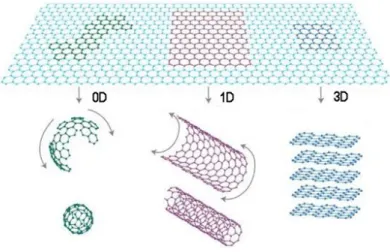
Graphene is a monolayer of sp2-hybridized carbon atoms arranged in a two-dimensional honeycomb lattice, firstly isolated from graphite in 2004 by Andre Geim and Konstantin Novoselov 7. It is the mother of all the other graphitic forms of different dimensions: fullerenes (0D), carbon nanotubes (1D) and graphite (3D) (Error! Reference source not found.).
Fig. 1.1. Graphene as building block for carbon materials of all other dimensionalities: 0D fullerenes, 1D carbon nanotube and 3D graphite. Adapted from 48.
The 2s and two 2p orbitals hybridize to form three sp2 planar orbitals that participate in covalent σ bonds. The fourth electron occupies the perpendicular
2
pz orbital and forms a delocalized π bond. The strong σ bonds are responsible of graphene mechanical properties, while the delocalization of π electrons gives rise to a high graphene electrical conductivity 49.
The first graphene flakes were isolated by mechanical exfoliation of highly oriented pyrolytic graphite using an ordinary scotch tape and transferred on a silicon substrate to fabricate a metallic field-effect transistor 7. Thanks to their “groundbreaking experiments regarding the two-dimensional material graphene”, Geim and Novoselov were awarded the 2010 Nobel Prize in Physics 50.
1.2 Graphene properties
Graphene shows peculiar electrical, thermal, optical and mechanical properties. Graphene films exhibit a pronounced ambipolar electric field effect such that charge carriers can be tuned continuously between electrons and holes in concentrations up to 1013 cm-2 and their mobilities (μ) can exceed 100000 cm2V-1s-1 even under ambient conditions 48. Graphene electrical properties derive from its band structure: it is a zero-gap semiconductor with a π-bands linear dispersion at the K points of the Brillouin zone, also known as the Dirac points (Error! Reference source not found.). Due to this l inearity, the charge carriers in the graphene have no rest mass and behave like relativistic particles 9,48.
3
Fig. 1.2. Electronic dispersion in the graphene lattice. Plot of the π-bands over the Brillouin zone, with a zoom-in of the energy bands in the vicinity of the Dirac point (ED). Adapted from 51.
In addition, graphene is the strongest material ever measured, with Young’s modulus of the order of 1 TPa and the intrinsic strength of 130 GPa 8. Furthermore it has other remarkable properties: high thermal conductivity up to 3000 W mK-1 near room temperature (RT) 52; impermeability at standard gases 53; optical transparency 54; outstanding mechanical flexibility and chemical durability 55; biocompatibility 56. These interesting properties make it suitable for different applications in nanoelectronics, transparent conducting electrodes, hydrogen storage 57,58, biomedical and sensing fields 59,60. In addition, properties and applications of vertical heterostructures composed of graphene and other 2D materials have been attracting a lot of attention in the fields of electronics and optoelectronics 61–63.
1.3 Graphene bioapplications
Graphene properties could be exploited in biosensing, drug delivery, antibacterial activity and imaging 64–67. Furthermore, transparency and flexibility properties, together with electrical conductivity, make it an
4
excellent candidate material for neural interfacing devices that combine stimulation and recording 28,29,68 and for tissue engineering applications 5,69,70. Graphene can be produced with different methods, resulting in different materials in terms of size, shape, number of layers, purity, lateral dimensions and chemical modification that can influence its applications 71. For example, GO and its chemical reduction known as rGO are usually preferred for biomedical applications thanks to the high water solubility and easy functionalization of the oxygenated species introduced during the oxidation processes 72,73. However, in GO the large fraction of sp3 carbon covalently bonded to oxygen to form epoxy and hydroxyl groups degrades the electronic performances of the material 74.
Highly crystalline graphene obtained via CVD has instead been mainly adopted for many applications including biosensing 75–77, stem cell differentiation 14 and neural electrodes 28,29.
One of the possible drawbacks in using GB materials in biomedical applications may be related to the unclear and highly debated cytotoxicity 78,79. It has been demonstrated that GO induced functional alterations in primary astrocytes 24 and cortical neurons 20. In spite of that, the potential cytotoxicity of graphene is often associated to disperse graphene flakes. Graphene flakes showed a shape and concentration-dependent cytotoxicity on PC12 cells 78, just as GO had a dose-dependent cytotoxicity in human fibroblast cells and mice 80. On the other hand, when GO is functionalized using different reducing agents, its toxicity can be drastically reduced 81,82.
5
1.4 Graphene in neural interfaces
In the past years, several studies have been conducted to investigate the use of GB materials as biocompatible neural interfaces 11,14,19–24,27,83–87
To date, most of the studies have investigated graphene covalent-functionalized forms such GO and rGO, or LPE graphene 10,17,19–23. GB materials can be used to design 3D scaffolds, in form of composites, foams, fibers and hydrogels to enhance their optical, electrical and mechanical properties, in a condition closer to the in vivo environment 70. With respect to those GB materials, pristine graphene, the defect-free layer of sp2 hybridized carbon atoms, offers enhanced electrical and tribological properties and most notably an excellent electrical conductivity. Thus, it can be possibly used as an electroactive scaffold that enhances neuronal regeneration and functional recovery 70.
The effect of GB materials on neural cells, even in the absence of any coating agent, has been investigated in many studies. An impairment of excitatory transmission was found in primary neurons following a chronic exposure to graphene oxide flakes 20,23. Bramini et al. observed that, even without interfering with neuron viability and intrinsic excitability, graphene exposure decreased the network electrical activity by creating an imbalance between synaptic excitation and inhibition 20. Rauti et al. showed similar results on primary hippocampal neurons. They reported that higher concentration of GO affected synapse formation and function without altering cell survival 23. It is important to notice that the previous studies employed a solution of graphene oxide. When a flat surface coated with graphene was used, the synaptic formation and network activity in hippocampal neurons were not altered 22. Uncoated graphene produced by LPE was reported to retain unaltered neuronal behavior, supporting neuronal functional development in
6
the absence of any perturbation of the neuronal network synaptic and electrophysiological properties (neuronal passive properties, spontaneous synaptic activity and short-term synaptic plasticity). Uncoated thermally reduced graphene (TRG) was shown to favor the multi-lineage differentiation of adult mouse olfactory bulb into neurons, astrocytes and oligodendrocytes. TRG supported the morphological differentiation of oligodendrocytes and the formation of functional synapses in neurons 21.
Graphene has also been interfaced with neural cells to exploit its applications in tissue engineering, as electroactive scaffold that can facilitate functional connection between neurons 69. Indeed, it has been demonstrated that conductive materials can enhance the electric field produced by the cell, influencing cell bioelectric properties 85. Electrical stimulation can also improve and direct neurite outgrowth 13,25 and can accelerate axonal elongation 5. Neural conductive interfaces for neural regeneration application usually exploit conductive polymers, such as polyethylenedioxythiophene (PEDOT) and polypyrrole (PPy), or composite materials whose conductivity depends on the inclusion of graphene or CNTs 6,16,18,25,26,88. Jakus et al. realized a 3D printable scaffold consisting of graphene with a minority of polylactide-co-glycolide that could be used as electrically conducting scaffolds for tissue regenerative engineering applications 16. Qian and colleagues fabricated a multi-layered porous scaffold composed of single-layered graphene or multi-single-layered graphene (MG) and polycaprolactone (PCL). The in vivo studies revealed that these substrates improves axonal regeneration and nerve remyelination after physical nerve injury, with a successful sensory recovery 18. Golafshan et al. developed a hybrid graphene nanosheets-sodium alginate/polyvinyl alcohol fibrous scaffold and observed an enhanced PC12 cells adhesion and proliferation 88. Additional researches supported the anti-inflammatory ability of 3D graphene foams, probably due
7
to their topographical structures, and the enhanced neural survival (neural stem cell and PC12) by the activation of microglia 89.
The use of pristine graphene with or without a polymeric coating is usually preferred to realize 2D devices, as planar electrodes to stimulate and record neural activity. Indeed, recently graphene and CNTs have been successfully used to improve recording and electrical stimulation of neurons 28,90 and surprisingly neural microelectrode arrays (MEAs) fabricated using graphene performed better than gold and indium tin oxide (ITO), in terms of signal-to-noise ratio (SNR) 91. Park et al. developed a graphene-based, carbon-layered electrode array (CLEAR) device that was implanted on rodent brain for high-resolution neurophysiological recording. Thanks to graphene biocompatibility, transparency and flexibility the CLEAR device showed long-term in vivo stability and viability for optogenetic activation of focal cortical areas, electrophysiology and cortical imaging 29. Kuzum and coauthors developed a transparent flexible neural electrode based on graphene for simultaneous electrophysiological recording and optical imaging, with an improved SNR and substantial reduction in electrical interference noise 28. The technique has been recently improved to integrate 2-photon microscopy, optogenetic, stimulation and cortical recordings in the same in vivo experiment 92. Recently, graphene has been also used to realize solution-gated field-effect transistor that were used to record visual and auditory responses in rats with performance similar to platinum black electrodes 30.
Polymer-coated graphene was also shown to enhance the differentiation of neural stem cells (NSC) into neurons rather than glia 14. Park et al. exploited graphene as a transparent electrode, observing a good electrical coupling between graphene and neurons for electrical stimulation and confirming the neural activity of the differentiated cells 14. The resulting neural network
8
functionality and the graphene effect on the maturation of the NSC’s electrophysiological state was also investigated by Guo et al. Graphene influenced both the passive and active bioelectric membrane properties, hyperpolarizing the resting membrane potential and increasing the firing of action potentials during development, resulting in an accelerated maturation and enhanced neural performance 85. In addition, coated GB materials were found to support the growth of primary hippocampal neurons, without affecting cell viability and morphology and accelerating neurite sprouting and outgrowth especially during the developmental phase 11.
Even in the absence of a coating, CVD graphene was shown to be biocompatible, sustaining neuron survival and neurite outgrowth. Bendali et
al. examined the survival and neurite outgrowth of adult retinal neurons both
on bare and polymeric coated graphene. They confirmed the graphene potential as a cytocompatible material for interfacing neurons with electronic devices, even if the presence of a polymeric coating seemed to help cell adhesion and spreading 87. Sahni et al. used bare graphene to culture cortical neurons and showed long, linear neurite growth and synapse-like structure formation. They reported also an increased adhesion of neurons on graphene, compared to the bare plastic dishes, that was explained by van der Waals overcoming the hydrophobic forces of the plastic dish 83. More recently, Pampaloni et al. have disclosed that single layer graphene boosts neuronal activity, increasing the action potential frequency in hippocampal neurons by altering extracellular ion distribution at the material interface. They hypothesized that potassium ions are trapped at the carbon surface, leading to a local depletion at the neuronal membrane 27. Also, it has been shown, that neural affinity strongly depends on the graphene quality. Veliev et al. showed that hippocampal neurons cultured on bare graphene had an improved adhesion and outgrowth, with a neuritic architecture similar to the
9
conventional coated controls. On the other hand, the use of defective graphene prevented cell attachment, demonstrating that the presence of carbon atoms alone does not guarantee the material cytocompatibility, but rather the material crystalline quality plays a crucial role 86.
It should be noted that most of the existent studies that use pristine graphene as a neural interface investigate its effect on central neurons. To date, the interaction between pristine graphene and peripheral neural cells has been scarcely investigated, even if graphene positive effect on neurite outgrowth and proliferation could open opportunities in neuroscience, neural engineering and regenerative medicine 12,31.
10
2 Graphene synthesis and characterization
In this Chapter, section 0 gives an overview of the different graphene synthesis methods. Section 2.2 describes the characterization techniques mainly used in this work to investigate the structural, chemical and electronic properties of the graphene substrates: AFM, scanning electron microscopy (SEM) and Raman spectroscopy. An extensive description of the synthesis methods used in this thesis – epitaxial growth on SiC and CVD on copper – is given in section 2.3 and 2.4 The different growth processes specifically developed and adopted in this work are described, together with the approaches used to improve graphene quality. Finally, the optimized transfer approach developed to increase graphene adhesion on glass is presented.
This chapter contains information published in the peer-reviewed work with authors D. Convertino, A. Rossi, V. Miseikis, V. Piazza, C. Coletti: “Thermal decomposition and chemical vapor deposition: a comparative study of multi-layer growth of graphene on SiC(000-1).” MRS Advances 1(55):3667–72 (2016). Experiments and data shown in each figure were performed and analyzed by D. Convertino.
Graphene samples were also produced and characterized for collaborations that has led to the publication of numerous works cited in the chapter and coauthored by D. Convertino.
2.1 Graphene growth
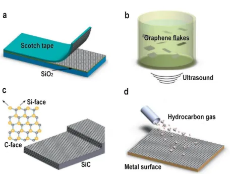
Since its first isolation in 2004, a great effort has been made by the research community to produce graphene with different methods that span from micromechanical exfoliation, to chemical-based approaches, to thermal
11
decomposition of silicon carbide and chemical vapor deposition on metals (Fig. 2.1).
Fig. 2.1. Schematic illustration of graphene synthesis methods. (a) Micromechanical exfoliation. (b) Liquid phase exfoliation. (c) Thermal decomposition of SiC. (d) Chemical vapor deposition on transition metals. Adapted from 93.
Micromechanical exfoliation consists in a repeated peeling of flakes of graphite using scotch tape (Fig. 2.1(a)) 7. The weak van der Waals interplanar interactions allow the isolation of single layers of graphene that can be transferred by simply pressing the tape onto another substrate. This graphene presents the highest quality level and it is preferred for fundamental studies thanks to its perfect crystallinity and low density of defects. However, the typical micrometric size of the exfoliated flakes makes them unsuitable for large-scale production and applications.
12
In LPE the exfoliation process is scaled up. The graphite is dispersed in a solvent, exfoliated using ultrasound and ultracentrifugated to remove the un-exfoliated flakes (Fig. 2.1(b)) 93. The principle of LPE can also be used to exfoliate GO. The obtained GO has to be reduced using thermal or chemical treatments. These graphene-like structures have degraded quality and purity, altered electronic structure and physical properties due to the variable fraction of sp2 and sp3 hybridized carbon atoms and are usually used to produce conducting films and composites 94.
The two main techniques for wafer-scale synthesis of high quality graphene are thermal decomposition of SiC (Fig. 2.1(c)) 95,96 and CVD of graphene on transition metals (Fig. 2.1(d)) 41,97,98. These techniques guarantee scalability and cleanliness, preserving the graphene quality in terms of transparency and electrical conductivity and for these reasons were adopted in this work. Using thermal decomposition, the SiC wafer is annealed at high temperature leading to silicon desorption from the surface that leaves graphene layers behind 96. Graphene thus can be obtained directly on a commercially available semiconducting or semi-insulating substrate and no transfer is required. The SiC wafer is commonly cut in a way that produces the surface orientations (0001) and (0001̅), called the Si- and C-face, respectively. The choice of the SiC crystal face to grow graphene strongly influences the results 96. Indeed, thermal decomposition is not a self-limiting process and areas of different film thicknesses may exist on the same SiC crystal, especially on the C-terminated surface where the growth process is much faster and generates multilayered, rotationally disordered graphene 40. Prior to growth, both the surfaces are hydrogen etched to produce atomically flat surfaces 99. Moreover, hydrogen intercalation of graphene grown on the Si-face is used to better decouple the atomic-thick material from the substrate and to achieve charge neutrality 100.
13
The optimization of the growth process on both the crystal faces are discussed in detail in the following sections.
The chemical vapor deposition approach is a surface-mediated process that exploits the catalytic behavior of transition metals to synthesize both single-crystals and polycrystalline graphene, subsequently transferred onto many different substrates. Nickel is usually preferred to grow multilayer graphene. Due to the appreciable solubility of carbon in nickel, carbon diffuses into the metal and then segregates to form non homogeneous multilayer films of graphene 97. On the contrary, the low solubility of carbon in copper allows a self-limited growth that ceases as soon as the copper surface is covered with graphene. This results in a homogeneous single-layer film 41.
The two growth techniques to obtain large-scale highly crystalline graphene, namely thermal decomposition of SiC and CVD growth on copper, and the relative approaches specifically developed and optimized to produce the substrates used in this work will be described in detail in sections 2.3 and 2.4.
2.2 Graphene characterization
2.2.1 Atomic force microscopy
AFM is a scanning probe technique used for morphological characterization, force measurement and sample manipulation at the nanoscale. The principle of operation is to scan a flexible cantilever with a sharp tip back and forth across the sample’s surface with a feedback mechanism that enables a piezoelectric actuator to maintain the tip at a constant force or a constant height. A laser beam is focused on the cantilever and is reflected into a photodiode. During the scanning the cantilever bends and the laser beam deflection is measured by the photodetector. Typically, the AFM is operated
14
in three modes that differ from each other by the tip and sample interaction forces: non-contact mode (attractive force), contact mode (repulsive force) and tapping mode (the cantilever oscillates at its resonant frequency lightly tapping on the surface). AFM is capable of producing a three-dimensional topography with a nanometric resolution. In addition to topography also sample’s material properties and frictional forces can be detected by phase signal and lateral force signal respectively. Lateral force microscopy has been used for spatial mapping of frictional properties in partially graphitized SiC(0001) surfaces, providing a contrast between buffer layer and monolayer graphene 101. Moreover, the AFM phase sensitivity to material changes allows to distinguish between different numbers of graphene layers from the contrast change 102,103. In this work, the AFM images were taken using an AFM+ (Anasys Instruments) operated in tapping-mode using a standard tapping probe (PRE-EX-T125, Anasys Instruments). Typically, topography and phase channels were acquired to characterize the substrates.
2.2.2 Scanning electron microscopy
SEM is a technique that uses a focused high-energy electron beam to probe the sample surface. The interaction between the beam and the target sample generates electrons (e.g., either excited from the atoms of the sample or backscattered) that are used to gain information about the morphology and chemical composition of wide areas with a resolution of tens of nanometers. Indeed, secondary electrons and backscattered electrons, generated respectively by inelastic and elastic scattering interactions with the incident electron beam, are typically detected.
15
In this thesis, SEM imaging was performed at 5 keV using a Zeiss Merlin microscope, equipped with a field emission gun using an in-lens detector for secondary electrons.
2.2.3 Raman spectroscopy
Raman spectroscopy is a spectroscopic technique typically used to detect rotational, vibrational and other modes in a molecule. It measures the inelastic scattering generated by light interaction with the molecule. Each peak in Raman spectrum derives from a molecular or lattice vibration, giving information about molecular structure, crystallinity and residual stress. The characteristic graphene Raman spectrum has two main peaks associated with phonon vibrational modes: the G band (~1580 cm-1) and the 2D band (~2700 cm-1). In case of disordered samples there is also the D band (~1350 cm-1) 104,105. The G band originates from a first order Raman scattering process. The 2D band is associated to a double resonance electron-phonon inelastic scattering process. When the process involves a phonon and a defect, we have the D band.
The position and shape of the 2D peak give an indication of the number of graphene layers. In particular, the single Lorentzian fitting of the peak with a full width at half maximum (FWHM) of < 30 cm-1 is characteristic of monolayer graphene. In bilayer and trilayer graphene, the 2D peak becomes broader and the fitting requires multiple Lorentzians. Moreover the 2D band energy increases significantly with increasing layer number 106. In monolayer graphene, the 2D peak is two times more intense than the G peak. It has been demonstrated that the G to 2D band intensity ratio provides a good correlation with the number of graphene layers 107,108, even if considering the ratio alone could be not sufficient because it is also a benchmark for graphene doping 109.
16
Shifted G and 2D bands can also be associated with strain or doping or their combination 109–111. The energy of the 2D peak blue-shifts in p-type doping and red-shifts in n-type doping, with respect to the case of pure undoped graphene. While the G-band of graphene shifts towards higher wave numbers both n and p type doping 109,112. The separation of the strain and doping contribution from graphene’s Raman spectra is complicated, due to G (ωG ) and 2D (ω2D) band shifts dependency both on charges (n) and strain (ε). Lee et
al. proposed a method to extract the contribution of charges and strain in the
ωG - ω2D space using a vector model (Fig. 2.2) 110. They demonstrated that each experimental point (P) can be decomposed into two components, whose shift is due to strain (eT) or doping (eH) to extract the strain and doping values from known reference values. The eT and eH vectors divided the ωG - ω2D space in four quadrants: Q1 for compressive strains and hole doping, Q4 for tensile strain and hole doping and Q2 and Q3 that are not allowed, because both n- and p-type doping cause an increase in ωG.
Fig. 2.2. Vector model to separate the effect of doping and strain in graphene. The green dot (O) represents the point (ωG0, ω2D0) that is not affected by strain and doping. The magenta line represents a strain-free graphene with varying doping (ε=0). The orange line represents doping-free graphene under uniaxial stress (n=0). Any experimental point (P) can be decomposed along the strain-free vector (eH) and the doping-free vector (eT). The blue and red lines are experimental trajectories for n-type and p-type graphene, respectively. Adapted from 110.
17
It has been demonstrated that the G and 2D band width can be used as a measure for the amount of nanometric scale strain variations. By analyzing the relation between the G and D line width, Neumann et al. found that the strain variations constituted a dominant contribution to the G and 2D lines broadening 111.
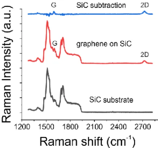
When graphene is grown on SiC, G and D bands are difficult to identify due to the Raman bands from the SiC substrate between 1200 and 1800 cm-1. The SiC contribution is usually removed by subtracting a reference SiC spectrum, making both the bands visible 113, as depicted in Fig. 2.3.
Fig. 2.3. Raman spectra of SiC, graphene on SiC and graphene on SiC after background subtraction.
When compared to micromechanically cleaved graphene, the 2D band FWHM of graphene on SiC is typically larger 106 and both G and 2D Raman peaks are strongly blue shifted (G band of ∼10 cm-1, 2D band ∼39 cm-1) due to the compressive strain caused by the SiC substrate 114. Differently from the 2D band, the G band position and FWHM are not influenced by the number of layers 106.
18
In this this thesis, all the Raman characterizations were performed using a micro-Raman spectroscope, equipped with a motorized sample stage (inVia Raman, Renishaw) and a 532 nm laser with a spot size of around 1 μm in diameter. The laser power was kept at 1 mW with an acquisition time of 2 s, unless otherwise indicated.
2.3 Epitaxial growth on Silicon Carbide
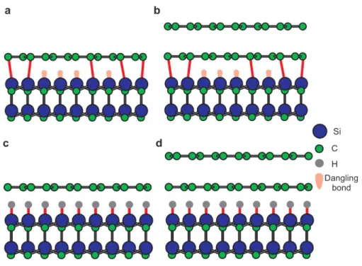
SiC can assume different crystal structures, called polytypes. In this work, we grow graphene on the hexagonal SiC polytypes 4H- and 6H-SiC because they provide an ideal crystallographic symmetry for the growth of graphene (Fig. 2.4). By cutting a hexagonal SiC crystal along a plane perpendicular to the c-axis, two surfaces are formed, one terminated by Si atoms, known as (0001) or Si-face and the other terminated with C atoms, known as (0001̅) or C-face (Fig. 2.4d). The growth of graphene has been carried out both on the Si-terminated and C-Si-terminated surfaces of the SiC crystal with different results 96.
19
Fig. 2.4. SiC crystal. (a) The building block of the SiC crystal is a tetrahedron of four carbon atoms covalently bonded to a silicon atom in the center. (b-d) The SiC4 tetrahedra forms the so-called bilayer and arranges in parallel planes of regular hexagonal networks whose stacking defines the different polytypes of SiC. (b) Hexagonal bilayer with Si and C in alternating tetrahedrally coordinated site. (c) Hexagonal frame of SiC bilayer. (d) Crystal structure of three different SiC polytypes: cubic 3C-SIC, hexagonal 4H-SiC and hexagonal 6H-SiC. The letter C or H denotes the cubic or hexagonal symmetry, while the number 3, 4 or 6 indicated the number of SiC bilayer within one stacking unit. One bilayer of Si and C has a ‘c’ dimension of 0.252 nm, that means that the 4H-SiC has a unit cell of 1 nm and the 6H-SiC of 1.5 nm 96,115. The cubic polytype (3C-SiC) has an ABC, while the hexagonal polytypes 4H- and 6H-SiC have a stacking sequence of ABCB and ABCACB, respectively. The Si-face and C-face of both 4H- and 6H-SiC are highlighted with red rectangles. Adapted from 115
2.3.1 Hydrogen etching
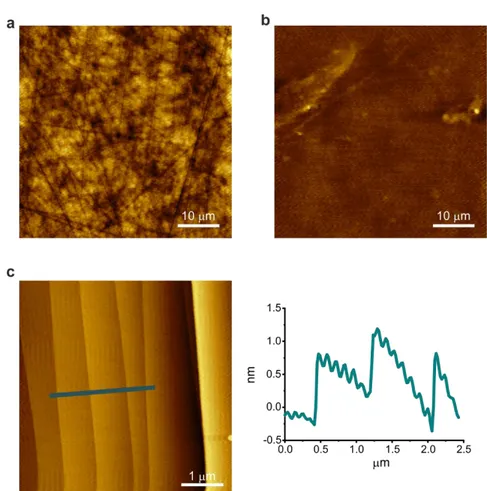
The crystalline quality of graphene grown on SiC by thermal decomposition strongly depends on the initial SiC surface quality. An as received optically polished SiC wafer usually presents high density of scratches on the surface arising from polishing damage (Fig. 2.5(a)). After a chemical mechanical polishing (CMP) the surface morphology is improved, but some residual polishing defects still remain (Fig. 2.5(b)). Hydrogen etching of SiC has been proposed as a method to reduce crystalline defects and achieve large atomically flat surfaces 99. Due to the unintentional miscut of the surface even
20
in on-axis substrates, the etching process produces a regular step array (i.e., reveals the atomic steps of the SiC surface), as shown in Fig. 2.5(c). On these atomically flat surfaces can be subsequently grown graphene of high crystalline quality 95.
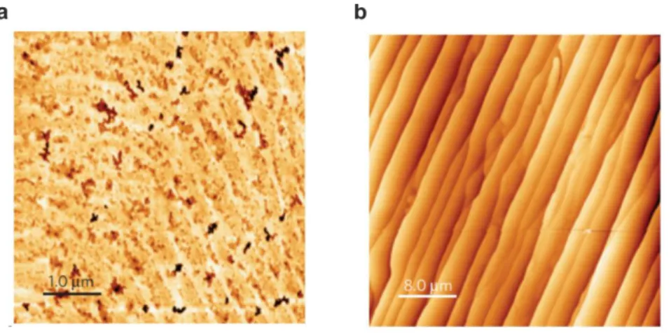
Fig. 2.5. AFM images of 4H-SiC wafer. (a,b) Before and (c) after hydrogen etching. (a) Optical polished C-face presents damages and deep scratches. (b) Chemical mechanical polished epi-ready Si-face SiC substrate is characterized by reduced roughness but still shows some polishing damages. (c) Hydrogen etched Si-face surface with atomically flat micrometric terraces separated by step (left). Step profile taken along the step flow reveals steps of unit cell height (1 nm) with an average distance of 1 µm (right).
In this work, we adopted hydrogen etching to etch both silicon and carbon basal planes of SiC crystals similar to what reported in Frewin et al. 116. To
21
this end, specific hydrogen etching processes were developed in our HT-BM Aixtron reactor. Etching was carried out by heating the samples under a flow of molecular hydrogen at a pressure of 450 mbar and at a temperature of around 1300 °C 44,117. The high temperature causes silicon atoms sublimation exposing the underlying carbon atoms. They react with the hydrogen atoms forming hydrocarbons that leave the surface. The process continues until several hundred nanometers of SiC are removed, improving the surface morphology. Indeed, for this work, the presence of atomically flat terraces was instrumental to exclude the effects of macroscopic topographical features of the samples on the cell culture. In this way, only the physicochemical effect of graphene could be evaluated excluding the morphology of the substrate underneath.
2.3.2 Graphene obtained via thermal decomposition of SiC
As mentioned above, the two different basal planes of the hexagonal polytypes of SiC, show significantly different growth modes for graphene 96. The graphitization process on the Si-face is characterized by the formation of an interface layer between the first graphene layer (monolayer graphene on SiC) and the underlying SiC substrate. This interface layer is known as zero layer or buffer layer and about 30% of the carbon atoms of this layer are covalently bound to the Si atoms of the Si-terminated substrate, with a periodicity of (6√3x6√3)𝑅30°. The growth mechanism of graphene on the Si-face is via step-edge nucleation, due to an increased Si evaporation at the step edges 118. Following Si sublimation, the buffer layer is released from the substrate as a new graphene layer and a new buffer layer is formed, maintaining the structure of the shifted interface layer, causing a 30° rotation of all the graphene layers with respect to the SiC substrate 119. Moreover the buffer layer has a significant electronic influence, reducing graphene mobility and originating an intrinsic electron doping (n≈1013 cm-2) 40.
22
While on the Si-face it is easier to grow homogeneous mono and few-layer (up to 3) graphene, on the C-face is difficult to control the number of layers as the thermal decomposition process appears to take place in a rather quick and uncontrolled fashion 96. In particular, the graphene layers typically obtained on the C-face lack a defined azimuthal orientation (i.e., turbostratic graphene) so that each layer behaves as an isolated graphene layer much less sensitive to SiC surface defects and is electronically decoupled from the neighboring ones. For this reasons, on this type of graphene, remarkable carrier mobilities have been measured 120. In this work, we developed specific growth processes to obtain graphene on both SiC faces with atomic thickness and conclusively selected the ideal surface for our neural interface studies.
2.3.2.1 Graphene on the C-face of SiC
Knowing the difficulties to control the number of graphene layers on the C-face via conventional thermal decomposition growth, we developed a tailored CVD approach to improve the graphene surface topography and the uniformity of the layer thickness distribution. For subsequent neural interface studies in fact homogenous graphene samples shall be preferred to identify the physicochemical effect of graphene on cells. In the following text we report the comparison of the structural, chemical and electronic properties of the graphene obtained on the C-face of SiC with the two approaches (i.e., conventional thermal decomposition vs. CVD).
Following hydrogen etching, multi-layer graphene was grown on the C-face via thermal decomposition and via CVD. Like hydrogen etching, growth was carried out in a commercial resistively heated cold-wall reactor (HT-BM Aixtron reactor). Thermal decomposition was achieved by heating the samples in argon (Ar) atmosphere at a temperature of 1350 °C and a pressure of 780
23
mbar for 15 minutes, similar to what described in 40 and in our previous works 121–124. CVD growth was achieved using methane (CH
4) as carbon precursor. Preliminary experiments were performed to optimize the growth process and it was found that addition of hydrogen in the gas mixture helped to reduce the formation of defects and to improve the homogeneity of the layer distribution. The sample was annealed at about 1350 °C within a 50% Ar and 50% H2 atmosphere held at 780 mbar, while flowing 3 sccm of CH4 for 5 minutes, similar to the procedure reported in our study 125.
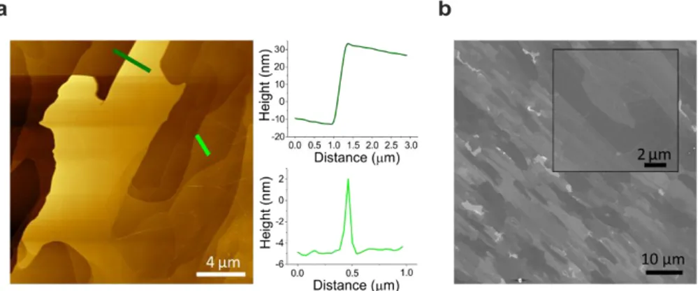
After the thermal decomposition process, AFM analyses revealed a surface topography similar to that reported in previous works 126,127. As shown in Fig. 2.6(a) and in the related line profile, pleats (or ridges) 2 to 10 nm high were observed. Such features are typically retrieved on graphene on SiC(000-1) (whereas they are not found on epitaxial graphene on SiC(0001)) and are due to the differences in expansion coefficients of SiC and graphene and to their weak coupling 126. Most notably, the surface displayed a significant step bunching as visible in the representative AFM micrograph reported in panel (a). The related line profile shows a step with a height of about 40 nm. Adjacent micron-sized domains with different heights were also evidenced by the different grayscale contrast in the SEM micrograph in panel (b) and were found to be similar to those described previously 128,129. Indeed, our growths further confirmed that thermal decomposition on the C-face takes place in a quick and uncontrolled fashion, thus yielding a relatively inhomogeneous surface. Although we found that the use of atmospheric pressure yields improvements with respect to the submicrometers domains typically obtained with UHV processes 44, the low surface energy of the C-face and the lack of a “growth enclosure” 129 most likely contributed to the obtained canyon-like morphology.
24
Fig. 2.6. Graphene grown by thermal decomposition. (a) AFM topography. Inset: profile analysis of a big step (top) and a ridge (bottom). (b) SEM image. Inset: high magnification of the same sample. Adapted from 44
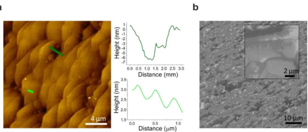
In the CVD grown samples, instead, differently from the thermal decomposition samples, the step-flow morphology was observed to be well-preserved and no dramatic variation in height within adjacent areas was observed, as reported in Fig. 2.7(a). Locally, one could appreciate inclusions of domains with an increased roughness (although still in the few-nanometers range). The representative SEM micrograph in Fig. 2.7(b) shows such inclusions as areas with a darker grayscale contrast. These inclusions most likely arise by a non-perfected CVD growth yielding the formation of sub-micrometer sized single-crystal domains. The grain size could possibly be increased by using higher hydrogen partial pressure during growth, an approach that needs to be investigated further.
25
Fig. 2.7. Graphene grown by CVD. (a) AFM topography. Right insets: profile analysis of a rough area (top) and atomic steps (bottom). (b) SEM image. Inset: high magnification of the same sample. Adapted from 44
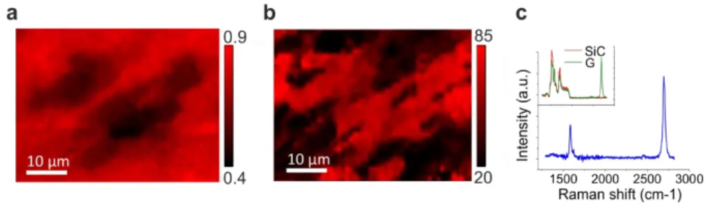
We estimated the graphene thickness for the two different processes via Raman spectroscopy by measuring the attenuation of the representative SiC peak measured at ~ 1516 cm-1. This peak is an overtone of the L point optical phonon and is attenuated in intensity when graphene overlayers are grown 130. The remaining fraction of the substrate intensity after graphene growth is indicated as S and calculated as the multiplication needed to normalize the selected SiC peak in the bare SiC substrate to that of the graphene sample. The thickness (t) of the graphene overlayers is calculated as t = -ln(S)/2α where α is graphene’s absorption coefficient. Fig. 2.8 and Fig. 2.9 reports micro-Raman maps of the ratio S (panel (a)) and of the 2D-peak full width at half maximum (FWHM) (panel (b)) of the same area of a typical thermal decomposition sample and CVD sample, respectively. Values of S close to unity indicate a low attenuation and are therefore indicative of few-layer graphene. Instead, S values closer to zero are found for areas with thicker multilayer graphene.
In the map of the thermal decomposition sample in Fig. 2.8(a), the fractional SiC Raman signal S ranges from 0.9 to 0.4, thus indicating that the number of
26
layers varies between 3 and 23. The 2D peak can be fitted with one Lorentzian, indicating a non-Bernal-stacked structure 131 with FHWM ranging from ~25 cm-1 to ~90 cm-1. Areas with higher attenuation of SiC (lower values of S in Fig. 2.8(a)), due to an increased thickness of graphene, correlate well with wider 2D FWHM as previously reported in 131. A characteristic spectrum after the subtraction of a reference SiC is shown in panel (c). The G peak was found at ~1580-1585 cm-1 and the 2D peak at ~ 2690-2720 cm-1, both position ranges are comparable to those reported for similar samples in previous works 120,131. Furthermore, absence of the disorder-induced D peak indicates high crystallinity of the grown graphene. Despite the good crystallinity, we evaluated such graphene samples as not suitable for the neural studies of this work due to the poor thickness control and canyon-like morphology.
Fig. 2.8. Raman characterization of graphene grown by thermal decomposition. (a) Fractional SiC Raman signal (S) and (b) 2D FWHM Raman mapping. (c) Raman spectra of graphene after SiC signal subtraction (blue color). Inset: original spectrum without subtraction (green color) and SiC reference signal (red color). Adapted from 44.
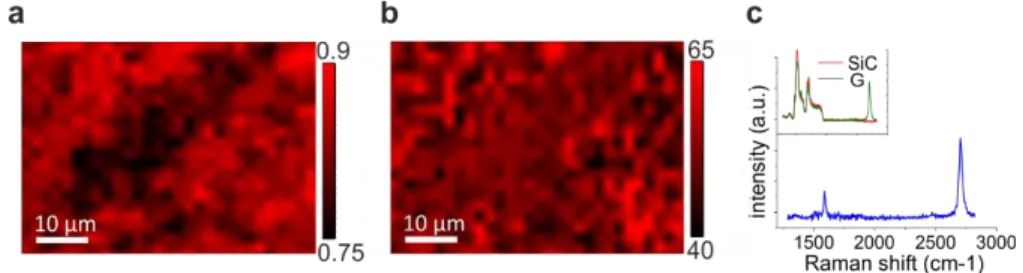
The Raman mapping of S (a) and of the FWHM of the 2D peak (b) of a typical CVD-grown sample is showed in Fig. 2.9. In this case, the value of S was found to vary between 0.9 and 0.7, which indicates a much narrower graphene thickness distribution, ranging from 3 to 7 layers. As for thermal decomposition samples, the 2D peak can be fitted well with a single
27
Lorentzian presenting a FWHM ranging from ~40 cm-1 to ~60 cm-1. A characteristic spectrum after the subtraction of a reference SiC is shown in panel (c). The G peak was found at ~1580-1595 cm-1 and the 2D peak at ~ 2690-2720 cm-1. The larger variation in the G peak position observed in the CVD samples might be indicative of graphene doping and needs to be investigated further. The D peak was generally absent and found only very occasionally, in spectra presenting a low 2D peak. This indicates that also in this case a high crystallinity is achieved.
Fig. 2.9. Raman characterization of graphene grown by CVD. (a) Fractional SiC Raman signal (S) and (b) 2D FWHM Raman mapping. (c) Raman spectra of graphene after SiC signal subtraction (blue color). Inset: original spectrum without subtraction (green color) and SiC reference signal (red color). Adapted from 44.
By adopting a similar CVD process, a high number of graphene layers (up to 90) with good crystallinity were synthesized, which were used for investigating absorption in the THz 125,132. As these samples were found to display saturable absorption, CVD-grown multi-layer graphene on SiC(000-1) might represent a favorable platform for the implementation of novel graphene-based mode-locked THz lasers 125.
Even if the CVD approach helped in improving thickness homogeneity and crystallinity, for cell culture experiments we decided to use graphene grown