Reconfigurable Logic Interface
Architecture for CPU-FPGA
Accelerators
Farnam Khalili, Marco Procaccini
,1,
Roberto Giorgi,
Department of Information Engineering and Mathematics, University of Siena, Via Roma 56, 53100 Siena, Italy
ABSTRACT
Programmable System-on-Chips (SoC) are a flexible solution to offload part of the compu-tational power from CPU to FPGA and accelerate the execution time. In today ARM-based SoCs, CPU and FPGA are usually connected to each other through several different communication links based on AMBA standard. This paper presents two possible design as reconfigurable logic inter-face architectures to be employed as a high performance interinter-face module in programmable logic accelerators. These designs provide us with programmability for bidirectional data communica-tion paths between CPU memory-mapped master interface and FPGA. Our first proposed design offers up to 32 configurable registers while the other has up to 32 configurable FIFOs to be able to exchange larger data. Both of these architectures communicate to programmble logic accelerators through the data stream channels.
KEYWORDS: Accelerator Interface; Reconfigurable; FPGA; SoC
1
Introduction
Applications of embedded intelligene is steadily growing due to various user programs and evolution in markets like smart phone, tablets, cars, smart wearable devices and etc. For instance, using face recognition algorithms on smart phones [OMTMSP+17] or
digi-tal signal processing methods in autonomous modern cars [Ger17] invoke a formidable processing power for such big data. Generally, a RISC or ARM processor can not provide enough computional power to process this large number of data. In this respect, the use of an exclusive co-processor such as DSP[SGH+17] or dedicated hardware accelerator is
in-dispensable. However, the latter performs efficiently the same functionality faster with less power consumption and silicon area. As a matter of fact, today FPGA SoCs [MF17] offer CPU alongside with FPGA fabric to efficiently increase the performance of an embedded system by decoupling the processing of big data from execution cycles and accelerate over-all performance of the application. Moreover, exploit of hardware level parover-allelism in high
performance computing such as Data-Flow threads [GF14, GPP07] or Data-Flow Proces-sors [KA17] are growing and evolving recently. As such, using SoCs due to their low NRE (Non-Recurrying Engineering), reliability and efficiency is a wise solution for researchers to evaluate their computing models. Therefore, there is a need for interfaces that are capable of exchanging these data between the FPGA fabric and the CPU. In such platforms there are several communication links each of which has specific features in terms of path delay and bandwidth [SWWB13] In this work, two configurable logic interface architectures are proposed to be used as the slave of CPU on Memory-Mapped (MM) standard buses like Avalon/AXI. These design offer a programmable bidirectional data path between CPU and FPGA to facilitate the system for the accelerator designers.
2
MM Configurable Interface Architecture
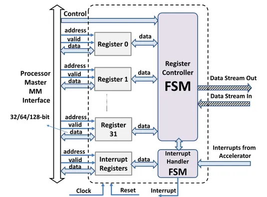
Figure 1 ilustrates proposed interface architecture to be employed between CPU and FPGA. This architecture is implemented in VHDL and tested on the AXIOM board [Gio17, MAB+16]
which has a Xilinx Ultrascale+ MPSoC. The design is packaged to IP-XACT through which user can set the data widths and number of registers. As one of advantages of this design is setting the write/read access of registers at run time through the Control signal by software application. Hence, each registers could have write access from both CPU-FPGA at the same time while in High Level Synthesis (HLS) implemented version of MM registers there is no such a feature. Furthermore, the data path between the proposed design and accelerator is Data Stream through which all data from registers all packetized and sent to the accelerator or the data from accelerator are depacketized and passed to the corresponding register. In this context, the Data Stream interfaces provide a high throughput data exchange between accelerator and CPU. Additionally, an interrupt handler is localized to offer more function-ality to the accelerator which can support up to 64 events and enable interrupt signals for the CPU. Finally, the FSM is the main processing engine to handle these exchanges between Data Streams and status from accelerator and Memory-Mapped registers.
A FIFO-based Memory-Mapped interface architecture (Figure 2) is presented in order to support larger data exchange between accelerator and CPU. In this design, the size of FIFOs, data width and number of data paths (FIFOS and Data Stream interfaces) all are set through IP-XACT block configuration depending on the application needs.
3
Conclusion
In this work, two configurale MM interface architectures are proposed to be used between CPU and FPGA. The first design offers up to 32 programmable registers implemented in VHDL which are accessible in write/read mode from both CPU and FPGA while through HLS implemented version this is not possible. The second design offers similar functionality as with up to 32 programmable FIFOs. The designs are tested on the AXIOM board and is used as a high performance interface between CPU and a Data-Flow hardware scheduler in [MFR18].
Processor Master MM Interface address valid data address valid data address valid data Control Register Controller
FSM
data data dataData Stream Out
Clock Reset 32/64/128-bit Interrupts from Accelerator Interrupt Handler
FSM
Register 31 Interrupt Registers Register 1 Register 0 data address valid data Data Stream In InterruptFigure 1: MM Interface Architecture between CPU and Programmable Logic with up to 32 programmable registers. Data Stream paths are shown by arrows with upward diagonal patterns. Processor Master MM Interface FIFO 0 FIFO 31 FIFO 0 FIFO 31
FSM 0
FSM
31 address valid data address address data data empty emptyFSM 0
FSM
31 full full data data data data Data Stream 0 Data Stream 0 Data Stream 31 address valid data Clock Reset 32/64/128-bit Data Stream 31Figure 2: MM Interface Architecture between CPU and Programmable Logic with up to 32 programmable FIFOs. Data Stream paths are shown by arrows with upward diagonal patterns.
References
[Ger17] Mario Gerla. [keynote 1] internet of vehicles: From intelligent grid to au-tonomous cars. In Networking, Architecture, and Storage (NAS), 2017 Interna-tional Conference on, pages 1–1. IEEE, 2017.
[GF14] Roberto Giorgi and Paolo Faraboschi. An introduction to df-threads and their execution model. In Computer Architecture and High Performance Com-puting Workshop (SBAC-PADW), 2014 International Symposium on, pages 60– 65. IEEE, 2014.
[Gio17] Roberto Giorgi. Axiom: A 64-bit reconfigurable hardware/software plat-form for scalable embedded computing. In Embedded Computing (MECO), 2017 6th Mediterranean Conference on, pages 1–4. IEEE, 2017.
[GPP07] Roberto Giorgi, Zdravko Popovic, and Nikola Puzovic. Dta-c: A decoupled multi-threaded architecture for cmp systems. In Computer Architecture and High Performance Computing, 2007. SBAC-PAD 2007. 19th International Sym-posium on, pages 263–270. IEEE, 2007.
[KA17] Yevgeny Korsunsky and Moisey Akerman. Processing data flows with a
data flow processor, October 24 2017. US Patent 9,800,608.
[MAB+16] Somnath Mazumdar, Eduard Ayguade, Nicola Bettin, Javier Bueno, Sara
Ermini, Antonio Filgueras, Daniel Jimenez-Gonzalez, Carlos Alvarez Mar-tinez, Xavier Martorell, Francesco Montefoschi, et al. Axiom: A hardware-software platform for cyber physical systems. In Digital System Design (DSD), 2016 Euromicro Conference on, pages 539–546. IEEE, 2016.
[MF17] Cathal Murphy and Yao Fu. Xilinx all programmable devices: A superior
platform for compute-intensive systems. 2017.
[MFR18] Procaccini Marco, Khalili Farnam, and Giorgi Roberto. Title should be writ-ten ask marco about the title that what is the correct title of this paper. ACACES, 2018.
[OMTMSP+17] Jesus Olivares-Mercado, Karina Toscano-Medina, Gabriel Sanchez-Perez,
Hector Perez-Meana, and Mariko Nakano-Miyatake. Face recognition sys-tem for smartphone based on lbp. In Biometrics and Forensics (IWBF), 2017 5th International Workshop on, pages 1–6. IEEE, 2017.
[SGH+17] Georg Stemmer, Munir Georges, Joachim Hofer, Piotr Rozen, Josef Bauer,
Jakub Nowicki, Tobias Bocklet, Hannah R Colett, Ohad Falik, Michael Deisher, et al. Speech recognition and understanding on hardware-accelerated dsp. Proc. Interspeech 2017, pages 2036–2037, 2017.
[SWWB13] Mohammadsadegh Sadri, Christian Weis, Norbert Wehn, and Luca Benini. Energy and performance exploration of accelerator coherency port using xilinx zynq. In Proceedings of the 10th FPGAworld Conference, page 5. ACM, 2013.