CHEMICAL ENGINEERING
TRANSACTIONS
VOL. 43, 2015
A publication of
The Italian Association of Chemical Engineering Online at www.aidic.it/cet Chief Editors:Sauro Pierucci, Jiří J. Klemeš
Copyright © 2015, AIDIC Servizi S.r.l.,
ISBN 978-88-95608-34-1; ISSN 2283-9216
Development of Low-cost PV Devices by Using Nanocrystal
Ink of Light-absorbing CIGS Semiconductor Layer
Maria Freni
a, Rosalba Passalacqua
*
a, Siglinda Perathoner
a, Gabriele Centi
a, Catia
Cannilla
b, Francesco Frusteri
baDepartment of Electronic Engineering, Industrial Chemistry and Engineering, University of Messina, CASPE/INSTM and ERIC aisbl, V.le F. Stagno d’Alcontres 31, 98166 Messina, Italy
bCNR-ITAE, Salita Santa Lucia Sopra Contesse, 5, 98126 Messina, Italy [email protected]
Copper indium gallium diselenide Cu(In1-xGax)Se2 (CIGS) nanocrystals were successfully synthesized by "heating-up" process. Monodisperse nanocrystals with an average diameter of 13.6 nm and a size deviation of 3.4 nm were obtained. CIGS showed a chalcopyrite single phase with the desired stoichiometric composition. In this work, we report high quality semiconductor nanocrystal films obtained by non-vacuum, facile and cheap procedure of synthesis and deposition. Thin films of CIGS (~ 100 nm in thickness) were obtained by nanocrystal dispersion in non-polar organic solvent and by spry-deposition of the resulting ink onto ITO conductive glass substrate without any post annealing treatment. Nanocrystals and their thin films were characterized by several techniques, such as TEM (transmission electron microscopy), EDX (energy-dispersive X-ray spectroscopy), XRD (X-ray diffraction), UV-vis-NIR absorption spectroscopy and photocurrent measurements. CIGS behave as light-absorbing layer in thin-film PV devices, the in solution-processability presented in this work and the possibility of large-scale synthesis enable the fabrication of thin films on light-weight and flexible plastic substrates, opening promising perspectives for producing cheaper and more efficient nanocrystal PV devices.
1.Introduction
In order to limit the dramatic environmental impact on the global climate changes due to the combustion of fossil fuels, alternative renewable and clean energy resources are required. Photovoltaics (PV) is one of the most promising among renewable energy technologies, PV devices convert sunlight directly to electricity, however its high cost compared to fossil fuels has still limited its use. Increasing devices efficiency and improving the manufacturing process in order to reduce PV electricity cost is a relevant objective to be achieved. One approach is to develop nanocrystal inks for obtaining inorganic thin films under ambient or mild processing conditions and deposit these light-absorbing semiconductor layers by simple techniques such as spray coating or printing (Stolle et al., 2013).
Cu(In1-xGax)Se2 (CIGS) is one of the most promising absorbing material used in thin film solar cell. This material possesses advantageous properties for solar applications: high absorption coefficient (~105 cm-1), good photostability, a direct band gap that is tunable in energy from 1.0 to 1.6 eV, depending on the gallium content. The conversion efficiency for CIGS-based solar cell fabricated by conventional vacuum process such as co-evaporation has reached ~ 20 % (Jackson et al., 2011). This process utilizes a series of processing steps accompanied by high production costs, large material losses, difficulty in achieving controlled stoichiometry and drawbacks due to the possible formation of intermetallic phases.
CIGS based thin films by non-vacuum methods have been developed in order to overcome these limitations, such as electrodeposition (Renganathan et at., 2011), spray pyrolisis, direct liquid coating, paste coating, etc. A reduction in energy and resource demand and in cost equipment are the advantages of these polycrystalline films so made. Recently a single-stage no-vacuum process based on CIGS nanocrystal chemical synthesis
DOI: 10.3303/CET1543117
Please cite this article as: Freni M., Passalacqua R., Perathoner S., Centi G., Cannilla C., Frusteri F., 2015, Development of low-cost pv devices by using nanocrystal ink of light-absorbing cigs semiconductor layer, Chemical Engineering Transactions, 43, 697-702
has been proposed (Cho et al., 2013). The nanocrystals are then dispersed in suitable solvents creating inks that can be deposited on a substrate by different techniques: spray deposition, roll coating, doctor blading, spin coating, drop casting, ink-jet printing or screen-printing (Hsu et al., 2011). Uniform and crack-free films, with controlled stoichiometry and crystal phases have been obtained.
The possibility to control size as well as nanocrystal composition offers the additional advantage of semiconductor band-gap modulation to maximize the conversion efficiency (Akhavan et al., 2012).
Akhavan et al. (2010 and 2012) reported that the photovoltaic devices constructed from CIS and CIGS nanocrystal inks showed still just a conversion efficiency up to 3 %.
Further improvements on both synthesis methods and film deposition techniques are necessary in order to have better film characteristics and increase device efficiency. The formation of monodisperse nanoparticles with single-phase stoichiometric CIGS is a key topic for fabricating high-quality thin films.
The synthesis techniques commonly used for nanocrystal preparation are “hot injection” and "heating-up". Hot injection is based on thermal decomposition of different precursors rapidly injected into a hot complexing solvent. Precursor order addition and temperature reaction can control nucleation and growth of nanoparticles (Hsu et al., 2011). However, hot-injection method presents scale-up difficulties for large quantities because the injection rate of monomers and metallic mass transfer are limited.
To overcome these difficulties, the simpler non-injection synthesis referred as heating-up was developed by Panthani et al. (2008) and modified by Chiang et al. (2011). By using this method, nearly monodisperse nanocrystals have been obtained by Hsu et al. (2011). The reaction solution is prepared at a low temperature and gradually heated to a higher temperature to synthesize nanoparticles.This method is more easily scalable because the synthesis can be carried out with high concentration of reactants in a large-volume reactor using the same quite mild and simple synthetic conditions.
Here, we report monodispersed and stoichiometric single phase CuIn0.8Ga0.1Se2.3 nanocrystals, synthesized by a modified "heating-up" method. After purification, the obtained nanocrystals were dispersed in hexane in order to form an ink. Uniform thin films were deposited onto ITO conductive glass substrate by ink spry-coating without any other post annealing treatments. The as-prepared CIGS thin films were tested as light-absorbing layer and preliminary results showing a good photocurrent response were performed.
2.Experimental
2.1 Nanocrystal Synthesis.
CuIn0.8Ga0.1Se2.3 nanocrystals were synthesized using a modified heating-up method. All operations were performed in air-free atmosphere to avoid degradation of reagents. A Schlenk line and a three-neck flask connected to it by a condenser were purged of oxygen and water by pulling vacuum for 1 h. In the three necks of the flask, a stopcock valve and two rubber septa are situated. The flask with closed stopcock valve was removed from the line and placed in a nitrogen-filled glovebox. 0.5 mmol of CuCl (0.0495 g), 0.45 mmol of InCl3 (0.099 g), 0.05 mmol of GaCl3 (0.0088 g), and 1 mmol (0.0789 g) total of elemental Se were added to 12 mL of oleylamine in the flask. The flask was again mounted on the Schlenk line under N2 atmosphere and placed on a heating mantle. In one of the rubber septa a thermocouple for temperature monitoring was positioned. The flask was purged again of oxygen and water by N2 bubbling at 110 °C for 30 min, then the temperature of the mixture was slowly raised to 260 °C and the reaction proceeds for 2 h under vigorous stirring. After the reaction flask was cooled to ambient temperature by a cold-water bath.
2.2 Nanocrystal purification and ink preparation
The nanocrystal products were isolated by precipitation with excess ethanol by centrifugation at 8000 rpm for 10 min and the supernatant containing unreacted precursors and byproducts was discarded. The nanocrystals were redispersed in chloroform and centrifuged at 7000 rpm for 5 min to remove poorly capped nanocrystals and large particulates. The precipitate was removed and, to ensure a good capping, a small amount (0.2 mL) of oleylamine was added to surnatant where nanocrystals remain dispersed. Ethanol was added to the particle solution, which is again precipitated by centrifugation at 8000 rpm for 10 min. This procedure of nanocrystal precipitation and redispersion was repeated two times to achieve a good purification. The yield of CIGS nanocrystals ranged from 30-50 % after two purification steps. The isolated nanocrystals were dispersed in hexane obtaining an ink. Nanocrystal ink was deposited by spray-coating using a commercially airbrush (Iwata) onto a glass substrate forming a thin film of ~ 100 nm.
2.3 Nanocrystal and ink characterization
- Transmission electron microscopy (TEM) analysis. To acquire and elaborate TEM images a Philips CM12 instrument equipped with a high-resolution camera was used. Nanocrystals were drop-cast from hexane dispersions on a carbon-coated copper grid.
- X-ray diffraction analysis were performed with a Philips X-pert 3710 X-ray diffractometer equipped with a Ni β-filtered Cu-Kα radiation at 40 kV and 20 mA. The nanocrystals were evaporated from concentrated dispersions onto quartz substrates. Data were collected over a 2ϴ range of 5-100 °, by scanning for 12 h, with a step size of 0.01 ° at a scan speed of 0.0021 °s-1. Diffraction peak identification was performed on the basis of the JCPDS database.
- Energy-dispersive X-ray analysis (EDX) were carried out with a scanning electron microscope Philips XL-30-FEG operating at an accelerating potential of 25 kV. Samples after solvent evaporation were fixed onto stub with a conductive graphite tape.
- UV-vis-NIR absorbance spectra were recorded in the 200-1200 nm range with a Jasco V-570 UV/VIS/NIR spectrophotometer using hexane-dispersed nanocrystals in a quartz cuvette.
- Photoelectrochemical measurements. Photocurrent measurements were performed to evaluate the functional characteristics of the nanocrystal based thin film samples. Chrono-amperometric tests were carried out at room temperature using an Autolab PGSTAT30 potentiostat/galvanostat in a standard three-electrode set-up with a saturated Ag/AgCl reference electrode, a Pt wire as counter and the nanocrystal thin film as working electrode. The sample photoresponse under front wall illumination was detected by irradiating the samples with a 300 W Xe-arc lamp equipped with an AM 1.5 G filter simulating solar light. 1 M KOH solution purged with N2 was used as the electrolyte.
3. Results and discussion
CIGS nanocrystals were successfully synthesized by a wet chemical "heating-up" synthesis process performed in oleylamine (OLA). Oleylamine is a long-chain primary alkylamine having a high boiling point (~350 °C). It has a multifunctional role for nanocrystal synthesis, acting as solvent, ligand and reducing agent. It is used as an activation agent that can expedite the precursors decomposition process and helps to eliminate their reactivity differences (Pan et al. 2009). OLA as organic capping ligand, forms complex compounds with the metal ions of the corresponding precursor at room temperature, leading to metastable compounds which can act as secondary precursors that can be thermally decomposed in a controlled way to yield nanoparticles. OLA dissolves and reduces Se powder forming Se species such as Se2-, Sex2-, depending on the reaction temperature.
Hsu et al. (2011) have prepared CIGS nanocrystals using heating-up method with chemical composition close to stoichiometric and they have found that phase formation sequence was CuSe → CuInSe2 → CIGS by progressive thermal decomposition of copper, indium, gallium, and -oleylamine complexes. Moreover, it forms stable dispersions in many solvents, complexing the final nanocrystals and preventing their aggregation. Therefore, its behaviour is useful in order to create stable inks (Chiang et al., 2011).
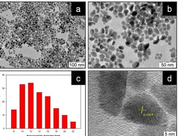
CuIn0.8Ga0.1Se2.3 morphology and size distribution were determined by TEM and statistical analysis. Figure 1 (a, b, d) shows that heating-up synthesis allows to obtain nanocrystals with good monodispersion and crystallinity.
Figure 1. (a, b, d) TEM images of the CuIn0.8Ga0.1Se2.3 nanocrystals at different magnifications (c) statistic
The nanocrystal shape is irregular and not perfectly spherical. Particle size distribution based on TEM micrographs is shown in Figure 1 c. Nanocrystal average diameter is 13.6 nm with a size deviation of 3.4 nm and a similar size was calculated by Scherrer equation based on the XRD (112) main peak. The estimated crystallite size was about 9.4 nm, which is close to the TEM result. High-resolution TEM image showed in Figure 1 d confirmed the chalcopyrite tetragonal phase with average distance of the crystallographic interplanar spacing of 3.34 Å which correspond to (112) crystal plane.
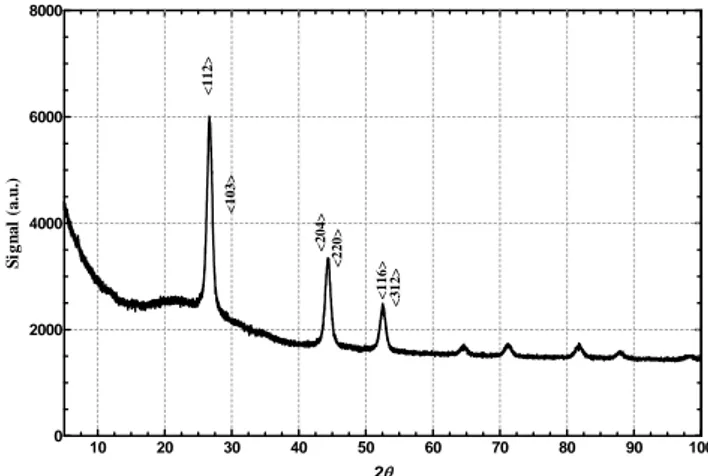
XRD pattern shows the formation of a pure chalcopyrite CIGS phase. The indexing of the peaks noted in the pattern correspond to the expected main peak position (112), (204)/(220), (116)/(312) of the chalcopyrite compound.
Figure 2. XRD pattern of CIGS nanocrystals.
The chemical compositions of CuIn0.8Ga0.1Se2.3 determined by EDX was reported in Table 1.
Table 1: CIGS composition by EDX analysis.
The analysis was performed on different nanocrystals and no variations have been observed. The atomic ratio Cu:In:Ga:Se was close to that calculated from the precursors weighed for the desired target compound. The presence of only four elemental components and sample purity is shown in the spectrum (Figure 3).
Figure 3. EDX spectrum of CuIn0.8Ga0.1Se2.3 nanocrystals.
Target Compound Composition measured by EDX (atom ratio % Cu/In/Ga/Se)
CuIn0.9Ga0.1Se2 23.94:18.82:2.47:54.78 (1:0.8:0.1:2.3) 10 20 30 40 50 60 70 80 90 100 0 2000 4000 6000 8000 <1 1 2 > <2 0 4 > <2 2 0 > <1 1 6 > <3 1 2 > * <1 0 3 > 2θ S ig n a l ( a .u.)
The UV-Vis absorption spectrum of CIGS nanocrystal dispersion in hexane in the wavelength range 250-1100 nm is shown in Figure 4.
From the absorption spectrum, it was possible to determine the band gap of the synthesized CIGS nanoparticles using the Tauc relation (Tauc, 1974): (αhν) = A·(hν - Eg)n, where A is a constant, α is the absorption coefficient, Eg is the average band gap of the material, and n depends on the type of transition. For direct band gap semiconductors, n = ½. The average band gap was estimated from the intercept of the linear portion of the (αhν)2 vs hν plot on the hν axis. The band gap value was determined to be about 1.27 eV. Therefore, it was concluded that the synthesized CIGS nanocrystals could be appropriate candidate as light-absorber material for thin film solar cells.
Figure 4. Absorption spectrum of CIGS nanocrystals dispersed in hexane.
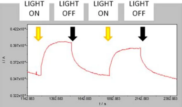
Nanocrystal ink was deposited by spry-deposition onto a ITO conductive glass (8-12 Ω/sq) and the resulting thin film was characterized by photocurrent measurements. CIGS are photoactive, as revealed by photocurrent analysis. Photocurrent response was measured by on-off cycles with dark conditions and under simulated AM1.5 G illumination (Figure 5) showing stability and reproducibility.
Figura 5. Transient photocurrent response of a CIGS thin film deposited on ITO glass substrate, recorded during two cycles of on-off made by irradiating the sample with simulated solar light.
Figure 6 reports the potentiodynamic plots (photocurrent (i) versus applied potential (E)) recorded in the range -1.5/+1.5 V highlighting the different behaviour of the CIGS thin film under illumination and in dark condition.
Figure 6. Linear sweep voltammetry (LSV) of a CIGS thin film deposited on ITO coated glass recorded with simulated solar light (red line) and under dark condition (black line).
-1.500 -1.000 -0.500 0 0.500 1.000 1.500 2.000 -1 -0.200x10 -1 0.050x10 -1 0.300x10 -1 0.550x10 -1 0.800x10 E / V i / A Wavelength (nm) 300 400 500 600 700 800 900 1000 1100 A b s ( a .u.) 0.0 0.2 0.4 0.6
4. Conclusions
A heating-up process, suitable to synthesize monodisperse CIGS nanocrystals with desiderate composition and crystal phase, was reported. The obtained nanocrystals were fully characterized and used to create inks for thin-film deposition by spray coating. CIGS nanocrystals can be appropriate candidate as light absorbing material for thin film solar cells. The results evidence high quality films of semiconductor nanocrystal obtained by non-vacuum, facile and cheap procedures of synthesis and deposition. The method is advantageous for large-scale nanocrystal production because the synthesis can be conducted using a high concentration of reactants in a large volume reactor and the spry-deposition technique can be applied to larger substrates. Therefore, the solution-processability of the technique and the possibility of a large-scale synthesis enable fabrication of thin films on light-weight and flexible plastic substrates, opening promising perspectives to produce cheaper and more efficient PV devices.
Acknowledgements
This work has been funded by MIUR by means of the national Program PON R&C 2007-2013, project “ENERGETIC - Tecnologie per l’ENERGia e l’Efficienza energETICa - PON02 00355".
References
Akhavan V.A., Goodfellow B.W., Panthani M.G., Steinhagen C., Harvey T.B., Stolle C.J., Korgel B.A., 2012, Colloidal CIGS and CZTS nanocrystals: A precursor route to printed photovoltaics, J. Solid State Chem. 189, 2-12.
Akhavan V.A., Harvey T.B., Stolle C.J., Ostrowski D.P., Glaz M.S., Goodfellow B.W., Panthani M.G., Reid D.K., VandenBout D.A., Korgel B.A., 2013, Influence of composition on the performance of sintered Cu(In,Ga)Se2 (CIGS) nanocrystal thin film photovoltaic devices, ChemSusChem 6, 481-486.
Akhavan V.A., Panthani M.G., Goodfellow B.W., Reid D.K., Korgel B.A., 2010, Thickness-limited performance of CuInSe2 nanocrystal photovoltaic devices, Energy Express 18, A411-A420.
Chiang M.-Y., Chang S.-H., Chen C.-Y., Yuan F.-W., and Tuan H.-Y., 2011, Quaternary CuIn(S1−xSex)2 Nanocrystals: Facile Heating-Up Synthesis, Band Gap Tuning, and Gram-Scale Production, J. Phys. Chem. C 115, 1592-1599.
Cho A., Ahn S., Yun J.H., Gwak J., Ahn S.K., Shin K., Song H., Yoon K.H., 2013, Non-vacuum processed CuInSe2 thin films fabricated with a hybrid ink, Sol. Energy Mater. Sol. Cells 109, 17-25.
Hsu W.-H., Hsiang H.-I., Chang Y.-L., Ray D.-T. and Yen F.-S., 2011, Formation Mechanisms of Cu(In0.7Ga0.3)Se2, Nanocrystallites Synthesized Using Hot-Injection and Heating-Up Processes, J. Am. Ceram. Soc. 94(9), 3030-3034.
Jackson P., Hariskos D., Lotter E., Paetel S., Wuerz R., Menner R., Wischmann W., and Powalla M., 2011, New world record efficiency for Cu(In,Ga)Se2 thin-film solar cells beyond 20%, Prog. Photovolt. Res. Appl. 19(7), 894-897.
Pan D., Wang X., Zhou Z.H., Chen W., Xu C. And Lu Y., 2009, Synthesis of quaternary Semiconductor Nanocrystals with tunable Band Gaps, Chem. Mater. 21, 2489-2493.
Panthani M.G., Akhavan V., Goodfellow B., Schmidtke J.P., Dunn L., Dodabalapur A., Barbara P.F. and Korgel B.A., 2008, Synthesis of CuInS2, CuInSe2, and Cu(InxGa1-x)Se2 (CIGS) Nanocrystal “Inks” for Printable Photovoltaics, JACS 130, 16770-16777.
Renganathan N.G., Subramanian M.V., Mohan S., 2011, Electrodeposition route to synthesize cigs films an economical way to harness solar energy, JESTEC 3(1), 206-212.
Stolle C.J., Harvey T.B. and Korgel B.A., 2013, Nanocrystal photovoltaics: a review of recent progress, Curr. Opin. Chem. Eng. 2, 160-167.