U
NIVERSITÀ DELLA
C
ALABRIA
Dipartimento di Ingegneria Informatica, Modellistica, Elettronica e Sistemistica
Dottorato di Ricerca in
Tecnologie dell’informazione e della comunicazione CICLO XXXI
TITOLO TESI
Reliability of GaN-based devices for Energy
Efficient Power Applications
Settore Scientifico Disciplinare ING-INF/01 Elettronica
Coordinatore: Ch.mo Prof. Felice Crupi Firma:
Supervisore/Tutor: Ch.mo Prof. Felice Crupi Firma:
Co-tutor: Ch.mo Prof. Lionel Trojman Firma:
Dottoranda: Eliana Maribel Acurio Méndez Firma:
iii
Declaration of Authorship
I, Eliana Maribel Acurio Méndez, declare that this thesis titled, “Reliability of GaN-based devices for Energy Efficient Power Applications ” and the work presented in it are my own. I confirm that:
• This work was done wholly or mainly while in candidature for a research de-gree at this University.
• Where any part of this thesis has previously been submitted for a degree or any other qualification at this University or any other institution, this has been clearly stated.
• Where I have consulted the published work of others, this is always clearly attributed.
• Where I have quoted from the work of others, the source is always given. With the exception of such quotations, this thesis is entirely my own work.
• I have acknowledged all main sources of help.
• Where the thesis is based on work done by myself jointly with others, I have made clear exactly what was done by others and what I have contributed my-self.
Signed:
v
“A dream you dream alone is only a DREAM. A dream you dream TOGETHER is reality.” Yoko Ono
vii
Abstract
The wide spectrum of power electronics applications, including their role in renew-able energy conversion and energy saving, require the innovation from conventional Silicon (Si) technology into new materials and architectures that allow the fabrica-tion of increasingly lightweight, compact, efficient and reliable devices. However, the trade-off between long lifetime, high performance and low cost in the emerging technologies represents a huge limitation that has gained the attention of different research groups in the last years.
Gallium Nitride (GaN) is a wide-bandgap semiconductor (WBGS) that consti-tutes an excellent candidate for high-power and high-frequency applications due to its remarkable features such as high operating temperature, high dielectric strength, high current density, high switching speed, and low on-resistance. Compared with its Silicon counterpart, GaN is superior in terms of high breakdown field ( 3 MV/cm), exceptional carrier mobility, and power dissipation. By taking into account other WBG materials such as SiC, GaN grown on Si substrates promises similar perfor-mance but at a much lower cost in the low to mid power and high-frequency range.
Since GaN allows size and weight device reduction due to a better relationship between on-resistance and breakdown voltage, it is suitable for a variety of appli-cations such as RF power amplifiers, power switching systems, sensors, detectors, etc. Especially, in the field of energy efficiency, GaN technology appears as a future successor of Si in power conversion circuits. However, some drawbacks related to technology cost, integration, and long-term reliability have to be overcome for its wide adoption in the power applications market.
One of the worst inconveniences of AlGaN/GaN High Electron Mobility Tran-sistors (HEMTs) is the normally-ON operation. Since a two-dimensional electron gas (2DEG) channel is formed at the AlGaN/GaN interface due to inherent mate-rial properties, a negative bias has to be applied at the gate to switch the device off. Among the proposed solutions to fabricate normally-OFF devices, the metal-oxide/insulator-semiconductor (MOS/MIS) structure with different insulators has shown remarkable improvements in gate leakage reduction and drain current in-crease. Also in AlGaN/GaN Schottky Barrier Diodes (SBDs), the introduction of a MOS structure to create a gated edge termination (GET) at the anode area has re-sulted in significant improvements in reverse diode leakage and forward diode volt-age. Nevertheless, the improvement in the device performance by the introduction of a dielectric could seriously affect the device long-term reliability since additional degradation in this layer and at its interfaces with AlGaN or GaN occurs.
In the case of conversion systems, power devices are continuously switched from an OFF-state condition at high drain bias to an ON-state condition at large drain current. Therefore, the reliability of GaN-based devices has to be proven for the complete ON/OFF operation. This dissertation focuses on providing a more com-prehensive analysis of two main reliability issues related to the dielectric insertion under the gate/anode stacks by analyzing the use of different dielectric materials and device architectures.
The first issue is the positive bias temperature instability (PBTI), which is re-lated to the degradation of electrical parameters when high gate voltages and tem-peratures are applied and is especially observed during the ON-state operation of the transistor. By using MOS-HEMT structures with different gate dielectrics (SiO2, Al2O3, and AlN/Al2O3), the impact of the stress voltage, recovery voltage and tem-perature on the device reliability is analyzed including the role of oxide traps and the interface states to provide physical insights into this mechanism.
The second phenomenon discussed in this thesis is the time-dependent dielec-tric breakdown (TDDB) observed on GET-SBDs during its OFF-operation. The per-colation model and Weibull distribution are used to understand this degradation mechanism. As a result, it has been demonstrated that the time to breakdown tBD is influenced by the GET structure (single vs. double), the passivation thickness, the preclean process at the anode region before the GET dielectric deposition and the capping layer. Finally, by using 2D TCAD simulations, the long-term reliability improvement has been related to the reduction of the electric field peaks at critical areas such as the GET corner and beneath the anode field plate.
ix
Sommario
Il nitruro di gallio (GaN) è un semiconduttore ad ampia banda proibita (WBGS) che costituisce un candidato eccellente per applicazioni ad alta potenza e ad alta fre-quenza grazie alle sue notevoli caratteristiche come alta temperatura operativa, ele-vata rigidità dielettrica, alta densità di corrente, eleele-vata velocità di commutazione e bassa resistenza.
Poiché GaN consente riduzioni di dimensioni e peso del dispositivo grazie a una migliore relazione tra tensione on e resistenza, è adatto per una varietà di appli-cazioni come amplificatori di potenza RF, sistemi di commutazione dell’alimentazione, sensori, rivelatori, ecc. Soprattutto nel campo di efficienza energetica, la tecnologia GaN appare come un futuro successore di Si nei circuiti di conversione di potenza. Tuttavia, alcuni inconvenienti legati al costo, all’integrazione e all’affidabilità a lungo termine della tecnologia devono essere superati per la sua ampia adozione nel mer-cato delle applicazioni di potenza.
Uno dei peggiori inconvenienti dei transistor ad alta mobilità di elettroni Al-GaN/GaN (HEMT) è l’operazione normalmente attivata. Poiché un canale bidimen-sionale a gas di elettroni (2DEG) è formato all’interfaccia AlGaN/GaN a causa delle proprietà intrinseche del materiale, è necessario applicare una polarizzazione nega-tiva al gate per spegnere il dispositivo. Tra le soluzioni proposte per fabbricare dis-positivi normalmente OFF, la struttura di ossido di metallo/isolante-semiconduttore (MOS/MIS) con diversi isolanti ha mostrato notevoli miglioramenti nella riduzione della perdita di gate e nell’aumento della corrente di drain. Anche nei diodi a bar-riera Schottky (SBD) AlGaN/GaN, l’introduzione di una struttura MOS per creare una terminazione del bordo gated (GET) nell’area dell’anodo ha portato a miglio-ramenti significativi nella perdita di diodo inversa e nella tensione di diodo diretta. Tuttavia, il miglioramento delle prestazioni del dispositivo mediante l’introduzione di un dielettrico potrebbe seriamente compromettere l’affidabilità a lungo termine del dispositivo poiché si verifica un ulteriore degrado in questo strato e nelle sue interfacce con AlGaN o GaN.
Questa dissertazione si concentra sulla fornitura di un’analisi più completa di due principali problemi di affidabilità relativi all’inserzione dielettrica sotto le pile di gate/anodi analizzando l’uso di diversi materiali dielettrici e architetture di dispos-itivi. Il primo problema è l’instabilità positiva della temperatura di polarizzazione (PBTI), che è correlata alla degradazione dei parametri elettrici quando vengono ap-plicate alte tensioni di gate e temperature e viene particolarmente osservato durante il funzionamento a stato ON del transistor. Utilizzando strutture MOS-HEMT con diversi dielettrici di gate (SiO2, Al2O3, e AlN/Al2O3), l’impatto della tensione di ten-sione, della tensione di recupero e della temperatura sull’affidabilità del dispositivo viene analizzato includendo il ruolo delle trappole di ossido e gli stati dell’interfaccia per fornire intuizioni fisiche in questo meccanismo.
Il secondo fenomeno discusso in questa tesi è la ripartizione dielettrica dipen-dente dal tempo (TDDB) osservata su GET-SBD durante la sua operazione OFF. Il modello di percolazione e la distribuzione di Weibull sono utilizzati per com-prendere questo meccanismo di degrado. Di conseguenza, è stato dimostrato che il tempo di rottura del tBDè influenzato dalla struttura GET (singola contro doppia), dallo spessore di passivazione, dal processo precluso nella regione dell’anodo prima
della deposizione dielettrica GET e dallo strato di capping. Infine, utilizzando simu-lazioni 2D TCAD, il miglioramento dell’affidabilità a lungo termine è stato correlato alla riduzione dei picchi del campo elettrico in aree critiche come l’angolo GET e sotto la piastra del campo anodico.
xi
Acknowledgements
First and foremost, I thank God Almighty for blessing and giving me the strength and courage that I needed to achieve this dream. During the inconveniences and difficulties, He was my light of hope and my refuge. This Ph.D. meant more than scientific work to me, it also represented a journey towards self-awareness of my strengths and weaknesses, which has become an invaluable treasure for my life. The summarized work in this thesis would not have been possible without the guidance and support from many people around me. Therefore, I would like to take this great opportunity to express my gratitude to all of them because they made this experi-ence unforgettable.
I would like to express my sincere gratitude to the most wonderful research ad-visor Prof. Felice Crupi, who gave me the opportunity to start this Ph.D. and encour-aged me through many research obstacles for the past three years with the patience that characterizes him. I really appreciate his guidance, expertise and significant feedback because his extensive knowledge and considerable background in semi-conductor and reliability fields greatly improved my research work.
Prof. Lionel Trojman, as my local supervisor at Universidad San Francisco de Quito (Ecuador), deserves special thanks for taking the time to give me personal-ized semiconductor lectures before I started this Ph.D. and for his continuous ad-vice, support, confidence, and motivation during this adventure.
I would also like to thank Escuela Politecnica Nacional (Ecuador) for financially supporting my research activities and my stay in Italy, Belgium, and Ecuador. I want to express my sincere thanks to all the professors and staff of the Physics Department for their support and cooperation during the period of this work. In special, I extend my heartfelt gratitude to Dr. Marco Bayas and Dr. César Costa for approving and promoting this Ph.D. as department heads.
In 2017, I had the opportunity to perform research at the Interuniversity Mi-croelectronics Centre (imec) in Leuven (Belgium) to expand my learning in GaN technology and I would like to deeply appreciate the opportunity from Dr. Stefaan Decoutere. Working with him and his expert GaN team members was doubtless an important experience because not only deepened my knowledge in GaN device characterization and reliability tests but also expands my education in advanced fab-rication process steps in this technology.
As the characterization engineer in the group and my daily supervisor at imec, Dr. Nicolò Ronch deserves my undying gratitude. I enjoyed working with him in the lab and learned a lot from our weekly meetings to evaluate my progress, and define future works. It was wonderful to have a researcher like him as my supervi-sor and my good friend at the same time. I would like to also thank the following GaN team members: Brice De Jaeger, Prof. Benoit Bakeroot, Dr. Steve Stoffels, Dr. Shuzhen You, Karen Geens, Dr. Niels Posthuma, Dr. Marleen Van Hove, Dr. Dirk Wellekens and the rest of the members of the Epi-GaN section.
Many thanks to Prof. Paolo Magnone (University of Padua) and Dr. Ferdinando Iucolano (STMicroelectronics) for their scientific criticism, their involvement in this
research, and their knowledge sharing during our fruitful discussions. It was def-initely my pleasure and valuable experience to work with them. Without doubts, their feedback highly enriched this work.
Friends are the family that one can choose and I have the best. Part of this ad-venture was to meet new people and make new friends. Therefore, I want to thank all the new friends that I made from Ecuador, Italy, Belgium and from around the world for encouraging me and lending me their helping hand during my studies. I am also very grateful to my longtime friends for cheering me up and for their sup-port to overcome personal difficulties even when an ocean separates us.
The words are insufficient to thank my family, which is a great pillar of whole-hearted support in my life. God blessed me with my caring and loving parents, Pablo and Lourdes, my beautiful sisters, Sheylla, Liseth, and Britanie, my adorable niece Emily, and my tender grandmother Blanca. This Ph.D. started just like a dream in my head, but all of you taught me that with effort and determination any dream can become true. My mom merits special mention because she is my role model. Her unlimited strength, sacrifice, perseverance, and willpower motivated me to explore my potentials and helped me to believe in myself since I was a child. Her uncondi-tional love shows me that does not matter how difficult the situations are, giving up is not an option and now I am so grateful for that lesson that allowed me to finish this Ph.D. journey.
Finally, these words are for you my dear Cristian: Thank you so much for your deepest love, for your support through the distance, for encouraging me to pursue my dreams and for holding my hands in my ups and downs. I still cannot believe how lucky I am to be your wife. I am eternally in debt to God for having you in my life. Your love was and is my greatest inspiration every day and makes me a better version of myself. I love you.
Thank you all, Eliana
xiii
Contents
Declaration of Authorship iii
Abstract vii
Sommario ix
Acknowledgements xi
1 Introduction 1
1.1 Modern Power Electronics . . . 1
1.2 Switching devices in power conversion systems . . . 3
1.3 Comparison of semiconductor materials for power applications . . . . 5
1.3.1 Bandgap(Eg) . . . 6
1.3.2 Critical Electric Field(Ecritical) . . . 7
1.3.3 Electron Mobility(µn) . . . 7
1.3.4 Saturated electron drift velocity(Vsat). . . 9
1.3.5 Thermal Conductivity(λ). . . 9
1.4 The Beginning of GaN in power electronics . . . 9
1.5 General limitations for a wide GaN-technology adoption . . . 10
1.6 Thesis content overview . . . 11
1.6.1 Thesis objective . . . 11
1.6.2 Thesis outline . . . 11
Chapter 2: GaN technology . . . 12
Chapter 3: Reliability study of MOS-HEMTs . . . 12
Chapter 4: Reliability study of GaN-based SBDs . . . 12
Chapter 5: Conclusion and outlook . . . 12
2 GaN Technology 13 2.1 Material Properties . . . 13 2.1.1 Crystal structure . . . 13 2.1.2 AlGaN/GaN heterojunction . . . 14 2.1.3 Substrates . . . 19 SiC . . . 19 Sapphire (Al2O3) . . . 20 Si . . . 20
2.2 GaN-based devices architectures . . . 20
2.2.1 AlGaN/GaN High Electron Mobility Transistors (HEMTs) . . . 20
Enhancement mode GaN-based devices . . . 21
2.2.2 AlGaN/GaN Oxide-Semiconductor (MOS) and Metal-Insulator-Semiconductor (MIS) HEMTs . . . 22
2.2.3 AlGaN/GaN lateral Schottky Barrier Diodes (SBDs) . . . 23
Au-free Gated edge termination (GET) SBDs . . . 23
2.3.1 Self-Heating . . . 25
2.3.2 Trapping Effects. . . 25
The kink effect . . . 26
Current collapse . . . 27
2.3.3 Reliability-related issues in GaN-based power switching devices 29 OFF-state related reliability issues . . . 29
ON-state related reliability issues. . . 31
SEMI-ON state related reliability issues . . . 32
2.4 Summary of this chapter . . . 32
3 Reliability study of MOS-HEMTs 35 3.1 On the recoverable behavior of PBTI in AlGaN/GaN MOS-HEMT. . . 35
3.1.1 Introduction and state of the art . . . 35
3.1.2 Device structure and experimental setup . . . 37
Initial stabilization . . . 37
Stress test . . . 39
Recovery test . . . 39
3.1.3 Stress phase results and discussion . . . 40
3.1.4 Recovery phase results and discussion. . . 43
3.1.5 Conclusions . . . 47
3.2 Reliability impact of AlN layer sandwiched between the GaN and the Al2O3layers in recessed AlGaN/GaN MOS-HEMTs . . . 48
3.2.1 Introduction and state of the art . . . 48
3.2.2 Experimental setup for the stress phase . . . 50
3.2.3 Experimental setup for the recovery phase . . . 51
3.2.4 General characteristics comparison. . . 53
3.2.5 Stress phase results and discussion . . . 54
3.2.6 Recovery phase results and discussion. . . 56
3.2.7 Conclusions . . . 58
3.3 Summary of the chapter . . . 59
4 Reliability study of GaN-based SBDs 61 4.1 Methodology for time-dependent dielectric breakdown analysis . . . . 61
4.1.1 General background in dielectric breakdown . . . 61
4.1.2 Time-dependent mechanism . . . 61
4.1.3 Stress experiments for TDDB data extraction . . . 63
4.1.4 Statistical TDDB data analysis . . . 64
4.1.5 Lifetime extrapolation . . . 69
4.2 Reliability Improvements in AlGaN/GaN GET-SBDs . . . 71
4.2.1 Introduction and state of the art . . . 71
4.2.2 Device fabrication . . . 73
4.2.3 Experimental procedure . . . 75
4.2.4 Results and discussion . . . 77
Structure dependence (GET region) . . . 77
Passivation thickness dependence . . . 79
Preclean process dependence . . . 83
Buffer impact on TDDB . . . 84
4.2.5 Conclusions . . . 85
4.3 Influence of GaN- and Si3N4- passivation layers on the performance of AlGaN/GaN GET-SBDs. . . 86
xv
4.3.2 Device fabrication . . . 88
4.3.3 Results and discussion . . . 88
General device characteristics . . . 88
Breakdown characteristics . . . 89
Temperature dependence of the leakage current . . . 91
Accelerated TDDB measurements . . . 93
4.3.4 Conclusions . . . 96
4.4 Summary of the chapter . . . 97
5 Conclusion and outlook 99 5.1 Conclusions . . . 99
5.2 Outlook. . . 101
Scientific Contributions and Awards 103
xvii
List of Figures
1.1 Historical evolution of power electronics [3]. . . 1
1.2 Application fields of power electronics [4]. . . 2
1.3 Importance of the research and development of power devices for more efficient and eco-friendly power systems. . . 2
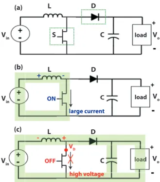
1.4 (a) Simplified schematic of a boost converter, which steps the DC volt-age up. (b) ON-state transistor operation (large drain current). (c) OFF-state transistor operation (high drain voltage). . . 3
1.5 Ideal and real I-V curves of a diode and a transistor during ON- and OFF-state operation [5], [6]. . . 4
1.6 Emerging WBDS (Silicon Carbide and Gallium Nitride) in power ap-plications. . . 6
1.7 Physical properties comparison between WBGS and Si. . . 6
1.8 Simplified energy band diagram of a semiconductor [12]. . . 7
1.9 Drift region width for each material at different breakdown voltages [12]. . . 8
1.10 On-resistance versus breakdown voltage for Si, SiC, and GaN [14]. . . 9
1.11 Increasing trend of the GaN power semiconductor market [21]. . . 10
2.1 Cubic zinc-blende (left) and hexagonal wurtzite (right) structure in III-Nitrides. The lattice parameters a, c and u are shown for the wurtzite structure [30]. . . 13
2.2 Spontaneous polarization orientation in Ga-face and N-face wurtzite structure [29]. . . 14
2.3 Energy band diagram for direct band gap GaN. The wavelength of an emitted photon is given by λ = hc/Eg where h represents Planck’s constant, c is the velocity of light, and Egis the bandgap energy. . . 15 2.4 A simplified representation of the lattice constant match of the AlGaN
on GaN layer and its induced strain in the basal plane (ε1) and in the growth (ε3) directions, which ultimately causes the piezoelectric polarization. . . 16
2.5 (a) Simplified scheme of the charge distribution in the AlGaN/GaN heterojunction and (b) the corresponding band diagram, where the in-terface discontinuity forms the quantum well that confines the 2DEG. Adapted from [35]. . . 17
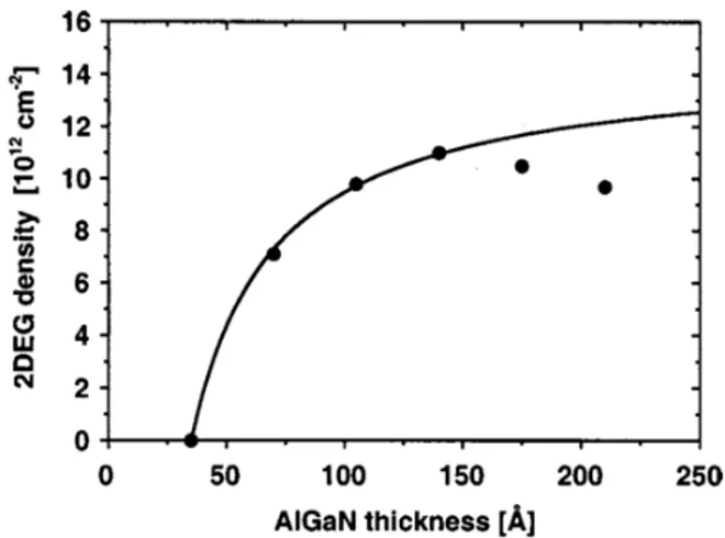
2.6 Schematic representation of the surface donor model when the un-doped AlGaN barrier thickness is (a) less than, and (b) greater than the critical thickness for the 2DEG formation (tCR) [34]. . . 17 2.7 Room temperature 2DEG density measured as a function of Al0.34Ga0.64N
barrier thickness. The curve is the least-squares fit of Eq. 2.6 to the tAlGaN <150 Ådata [34]. . . 18
2.8 Comparison of measured and theoretical calculation of the critical thickness for strain relaxation in the AlxGa1−xN/GaN heterostructure [36]. . . 19
2.9 Structure stack schema of (a) a multiple step-graded AlGaN and (b) an AlN/GaN superlattice buffer. . . 21
2.10 Simplified structure of an AlGaN/GaN HEMT during its (a) ON-state and (b) OFF-state operation. Adapted from [35]. . . 21
2.11 Aproaches to realize enhancement mode GaN devices [41]. . . 22
2.12 Schematic structure of (a) a Schottky gate AlGaN/GaN HEMT, (b) a GaN MOS-HEMT, and (c) a fully recessed GaN MOS-HEMT. It is worth mentioning that MOS-HEMT is a specific term when an oxide is used below the gate contact, while MIS-HEMT is the general term for all insulators. . . 23
2.13 Schematic illustration of (a) a forward biased and (b) a reverse biased GaN-based Schottky barrier diode (SBD) with their respective band diagrams.. . . 24
2.14 Schematic representation of (a) the conventional SBD and (b) the GET-SBD with a recessed AlGaN barrier to further reduce the reverse leak-age current [53]. . . 24
2.15 (a) Forward and (b) reverse DC curves of the GET-SBD (solid lines) and the conventional SBD (dotted lines), both with an anode finger width of 100 um [51]. . . 25
2.16 Possible traps position inside the AlGaN/GaN HEMT and their re-lated effects [58].. . . 26
2.17 Transistor output characteristics measured at two different values of VDS−max. The dashed line indicates VDS_kinkat each VGS[61]. . . 27 2.18 DC and pulsed I-V characteristics of an unpassivated AlGaN/GaN
HEMT on SiC substrate. Current collapse could be observed in the pulsed mode [62]. . . 27
2.19 Schematic representation of current collapse. Initially, surface donors are positively charged (ON-state). After electron trapping, surface donors become neutral and creates an extension of the depletion re-gion (virtual gate) (OFF-state). Finally. the captured electrons keep the channel partially depleted (ON-state) [37]. . . 28
2.20 Schematic structure of a passivated AlGaN/GaN HEMT by using Si3N4 to prevent a virtual gate formation [63]. . . 28
2.21 Normalized IDmax, RD, RS, IGstress, and IGo f f variation as a function of stress voltage in a step-stress experiment under VDS = 0 (VDG = 10−50 V in 1 V steps) [71]. . . 30
2.22 (a) Reverse gate step-stress test on five devices with a gate-to-drain distance of 0.7 µm where a VCRIT ICAL = −70 V was measured. (b) Gate current degradation by using stress gate voltages lower than the VCRIT ICAL[72]. . . 30 2.23 (a) Gate current monitored during TDDB experiments with three
dif-ferent stress voltages. (b) The corresponding distribution of the time to breakdown, which follows Weibull statistics [35]. . . 31
2.24 During ON-state regimes, the positive voltage applied to the gate stack favors the electron capture into the trap-states of the dielectric causing∆Vth [73]. . . 31
xix
2.25 The combination of high drain voltage and relatively high drain cur-rent during the SEMI-ON state allows the hot-electron injection and trapping into epitaxial defect-state [73]. . . 32
2.26 (a) Pulsed ID–VDcharacteristics acquired with constant quiescent VDS, and multiple quiescent VG. Dynamic RON worsens as VG > Vth. (b) The good correlation between IDSand dynamic RONincrease suggests hot-electron-related trapping mechanisms [73]. . . 32
3.1 Physical model of the influence of surface defect charge at AlGaN/GaN HEMT. (a) Electric field concentration at the gate edge. (b) Schottky barrier thinning [75]. . . 35
3.2 Overview of potential defect centers in the SiO2/barrier gate-stack of a GaN-based HEMT device [77]. . . 36
3.3 Schematic structure of the device under test (DUT). . . 37
3.4 (a) ID-VGScurve evolution and (b)∆Vth behavior during a stress test without an initial stabilization phase at room temperature (RT). It is worth noting that Vthinitially moves to more negative values, then it saturates and turns around. . . 38
3.5 Transfer curves in the linear regime for a virgin device, after the ini-tial stabilization and after successive stress-recovery experiments. No permanent damage is observed for the investigated stress voltages af-ter the recovery phase. . . 38
3.6 Testing procedure for the positive bias temperature instability (PBTI) analysis. . . 39
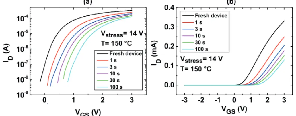
3.7 ID-VGScurves before (the initial stabilization was applied in the fresh device) and after successive stress experiments at VDS = 50 mV and high temperature in (a) a log-linear scale and (b) a linear-linear scale. The observed positive∆Vthshift indicates electron trapping. . . 40 3.8 Sketch of the band diagram for the stress phase (a) and the recovery
phase (b). During the stress phase, electrons from the 2DEG channel are trapped into the oxide traps, while during the recovery phase; electrons are released from the oxide traps. . . 40
3.9 Experimental (markers) and power-law fitting curves (lines) of the ∆th evolution during the stress phase at different stress voltages (a) and temperatures (b). In the investigated time window, an apparently good fitting with the classic power law model is observed. . . 41
3.10 The trapping rate parameter (Eq. 3.2) significantly decreases during the stress time (a), and by increasing stress voltage (b) and tempera-ture (c). . . 41
3.11 Trapping rate parameter b = ∂log(∆Vth)
∂logt as a function of the density of trapped charges at different stress voltages and temperatures applied to different samples (A, B and C). A clear universal decreasing behav-ior is observed. . . 42
3.12 Band structure of a SiO2/AlGaN-barrier/GaN-buffer stack. The AER (red area) is spanned by the applied forward gate bias and marks the energetic region, where defects can be filled due to forward gate bias [77]. . . 42
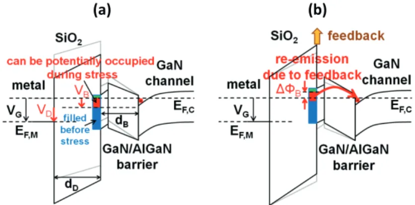
3.13 (a) The barrier potential is lowered from its thermal equilibrium value for VG > 0, thus electrons are trapped at the interface or at border defect states in the region below the channel Fermi level EF,C. (b) Charging of the interface increases φBand consequently, electrons can be re-emitted from the region lifted above EF,C[93]. . . 43 3.14 (a) Transconductance behavior during the stress phase by applying
different bias conditions. (b) Transconductance variation vs. ∆Vth af-ter different stress time and stress voltages at 150◦C. A linear correla-tion is observed (straight line). . . 43
3.15 Experimental (markers) and fitting curves based on Eq. 3.3 (lines) of the∆Vth evolution during the recovery phase for different (a) stress biases, (b) temperatures, and (c) recovery voltages. The fitting curves consist of the superimposition of two exponential functions. . . 44
3.16 Final fitting and individual contribution of trap 1 and 2 for the recov-ery data after a stress phase at Vstress= 14 V. . . 45 3.17 Both recovery time constants are independent of (a) stress voltage,
(b) decrease with temperature, and (c) increase with recovery voltage. The ratio between the two amplitudes is also (d) stress voltage inde-pendent, and gradually rises (e) with temperature and (f) recovery voltage. . . 46
3.18 β parameter evolution as a function of (a) stress voltage, (b) stress temperature and (c) recovery voltage. . . 46
3.19 Arrhenius plot of the recovery time constants extracted from the expo-nential fitting during the recovery phase. The two activation energies are obtained by the slope of the fitting lines.. . . 47
3.20 Apparent activation energy of the two traps (Ea1and Ea2) obtained in different samples (A, B, C, and D) at different recovery voltages. The activation energy of the faster trap (Ea1) exhibits a lower mean value and a higher dispersion. . . 47
3.21 Energy gap Eg versus dielectric constant e for various insulators and AlGaN compounds [109]. . . 49
3.22 Band lineups for SiO2, Al2O3, AlN, Si3N4, Al0.3Ga0.7N, and GaN [110]. 49 3.23 Voltage signal applied to the gate contact during the stress test. . . 50
3.24 ID-VGS curves before and after applying a pulse width of 0.1 µs in (a), (b) the single layer stack (Al2O3) and in (c), (d) the bilayer stack (AlN/Al2O3) at 50 ◦C and 150 ◦C, respectively. The ∆Vth is slightly influenced by the temperature during the stress phase. . . 51
3.25 ID-VGS curves before and after applying a pulse width of 0.1 µs in the AlN/Al2O3sample by using (a) a current criterion at 10 µA and VD=50 mV and (b) a current criterion at 100 µA and VD=500 mV. Sim-ilar behavior is observed in the Al2O3sample. . . 52 3.26 ID-VGScurves before and after applying a pulse width of 1, 30 and 100
µs (Al2O3). The∆Vth was evaluated by using the current criterion at 100 µA. . . . 52
3.27 (a) Voltage signal applied to the gate contact during the recovery test and (b) the respective drain current measurements for the two differ-ent pulse widths (1–30 µs) at 12 V in the single layer sample. . . . 53
3.28 Transfer characteristics in (a) AlN/Al2O3MOS-HEMT and (b) Al2O3 MOS-HEMT. . . 53
xxi
3.29 Normalized RONresistance as a function of the overdrive voltage VOV. The Al2O3MOS- HEMT exhibits a lower resistance than the AlN/Al2O3 device. . . 54
3.30 ID-VOV curve in (a) a linear-linear and (b) a log-linear scale obtained by applying a train of pulses with a period of 300 µs and width of 30 µs at the gate and drain terminals. The hysteresis observed was quantified by evaluating the shift at 0.1 mA.. . . 54
3.31 Experimental (markers) and fitting curves (lines) of the∆Vthevolution as a function of the width of the BTI stress pulse. These measurements were performed by following the procedure for the stress experiment described in subsection 3.2.2 . . . 55
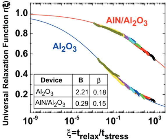
3.32 Experimental (markers) and fitting curves (lines) of the measured tran-sients fitted with the universal relaxation function (Eq. 3.10). . . 57
3.33 Initial ID-VGS curves (recovery sequence) before the application of each stress pulse at VOV=12 V in (a) the single and (b) double layer. The overlapping of all the initial curves confirms that no permanent degradation was observed during the experiments. . . 57
3.34 Experimental (markers) and fitting curves (lines) of the∆Vthrecovery evolution after applying a single stress pulse. The experiments were performed at 12 V and pulse widths from 0.1 to 300 µs. . . . 58
4.1 Schematic illustration of intrinsic oxide breakdown (SiO2) based on trap generation and conduction via traps (conductive path) [125]. . . . 61
4.2 Description and modeling of the oxide breakdown phases during a CVS [126]. . . 62
4.3 Schematic flow-chart describing the three lines of thought on neutral electron generation describe in the Literature [127]. . . 63
4.4 Monitored current through an oxide during CVS experiment in the case of oxide thickness (a) larger and (b) smaller than 5 nm [128]. . . . 63
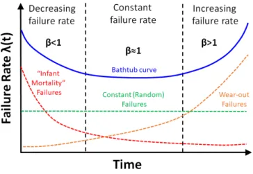
4.5 Schematic representation of the I-t traces and its noise during a CVS. Different time-to-breakdowns (tBD) can be extracted based on differ-ent criteria. tBD_a is extracted when the current exceeds a threshold (Ithreshold), tBD_bis extracted when a current jump is larger than a de-fined value (∆I) and tBD_c is extracted when the noise of the current goes beyond a threshold (Nthreshold) [126]. . . 64 4.6 The bathtub curve showing three categories over the device lifetime. . 66
4.7 Analysis of a TDDB experiment: (a) The tBD is extracted from the I-t traces; (b) the tBD values are firstly ordered from the smallest to the highest, then the cumulative failure distribution F(tBD_i)is calcu-lated; (c) F(tBD_i)is visualized in a Weibull plot to verify if the data are Weibull distributed and finally, the fitting parameters β and η are obtained [126]. . . 67
4.8 Weibull plot with two slopes (β) corresponding to the extrinsic and intrinsic failure modes [6]. . . 68
4.9 The tBD-Weibull slope (βtBD) vs. the number of traps N to form the percolation path. Since certain event to form percolation path could be caused by either N or N+1 traps, a transition region between the different levels is observed [128]. . . 68
4.10 Area scaling example. Under uniform degradation, the tBD distribu-tion measured on devices with different areas (A1, A2 and A3), nicely line up when they are scaled to a reference area (A1 in this case) [128]. 69
4.11 (a) Schematic Weibull plot under 3 different stress conditions result-ing in η1, η2 and η3. (b) Illustration of the long-term extraction of the tBD showing the easy scaling to any x% failure level to know the probability that x% of population fail under operating condition and vice-versa [126]. . . 70
4.12 (a) Leakage current and (b) forward characteristics of AlGaN/GaN SBD in floating and grounded substrate configurations [6]. . . 72
4.13 Leakage characteristics comparison of two device architecture (EET-SBD and GET-(EET-SBD) in the Au-free CMOS process developed by imec. A significant drop in leakage can be achieved by using the GET-SBD architecture [6]. . . 73
4.14 (a) Simplified schematics of AlGaN/GaN GET-SBDs used in this study. The detailed cross sections show GET with (b) single and (c) double structures. . . 74
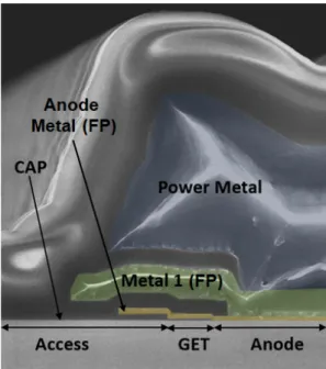
4.15 Cross-sectional SEM image of the fabricated GET-SBD. . . 75
4.16 (a) Forward and (b) reverse characteristics of the AlGaN/GaN GET-SBD.. . . 76
4.17 Dispersion measurement at (a) room and (b) elevated temperatures. Pulsed I–V measurements were performed with a Keysight B1505A. Graph legend: OFF-state biases.. . . 76
4.18 Typical results of DC breakdown measurements in the analyzed sam-ples where the double-GET structure shows the highest VBD. . . 77 4.19 Results of CVS experiments for one stress condition in single- (REF)
and double-GET (DOUBLE GET) structures. . . 77
4.20 Weibull distribution for different stress conditions in (a) single-GET (REF) and (b) double-GET (DOUBLE GET) devices. . . 78
4.21 Time to have 63.2% failures in the single-GET structure for the break-down mechanisms with β=3 and β=5. . . 78
4.22 (a) Reverse DC bias sweep with the substrate floating and grounded in double-GET devices. (b) CVS experiments in lateral isolation struc-tures. . . 79
4.23 Line profile of the absolute electric field within the AlGaN barrier (3 nm below the top surface in the recessed portion). The double-GET structure adds a new peak which alleviates the peak at the GET corner. 80
4.24 Results of CVS experiments for one stress condition in thick- (REF) and thin-passivation (THIN PASS) structures.. . . 80
4.25 Weibull distribution for different stress conditions in (a) thick- (REF) and (b) thin-passivation (THIN PASS) devices. . . 81
4.26 Time to have 63.2% failures in thick- (REF) and thin-passivation (THIN PASS) diodes for the breakdown mechanism with β∼3. . . 81
4.27 Line profile of the absolute electric field within the AlGaN barrier (3 nm below the top surface in the recessed portion). The thin-passivation structure reduces the peak at the GET corner. . . 82
4.28 Arrhenius plot of tBDof the 63.2% of the population (η) in thick- (REF) and thin-passivation (THIN PASS) devices. . . 82
4.29 Results of CVS experiments for one stress condition in diodes with a more aggressive preclean treatment. . . 83
4.30 Weibull distribution for different stress conditions in (a) thick- (REF) and (b) thin-passivation (THIN PASS) devices. . . 83
xxiii
4.31 (a) Reverse DC bias sweep and (b) temperature dependence of the VBD by keeping the substrate floating and grounded in 2 GET-THIN devices. . . 84
4.32 tBD-distribution obtained from the CVS measurements under the same stress condition for devices described in Table 4.2. . . 85
4.33 Absolute electric field within the AlGaN barrier (3 nm below the top surface in the recessed portion). The 2GET-THICK structure distributes the electric field more uniformly by adding a new peak (2-GET) and by reducing the peak beneath the field plate (FP). . . 86
4.34 (a) Simplified schematics of AlGaN/GaN GET-SBDs used in this study. The detailed cross sections show GET with (b) single and (c) double structures. . . 88
4.35 Dispersion measurements in devices with (a) Si3N4and (b) GaN cap layer at room and elevated temperature. A slight reduction in RON -dispersion is observed in Si3N4cap devices. . . 89 4.36 DC reverse sweep at different temperatures in (a) Si3N4 and (b) GaN
cap devices with the substrate grounded and floating. . . 90
4.37 The extracted VBD in both devices shows a negative temperature co-efficient. Closed symbols: substrate grounded. Open symbols: sub-strate floating. . . 90
4.38 Activation energy plot of the leakage current of AlGaN/GaN SBDs with (a), (c) Si3N4 and (b), (d) GaN as cap layer with the substrate grounded and floating, respectively. . . 91
4.39 Evolution of the activation energy with the reversed voltage in (a) Si3N4 and (b) GaN cap devices when the substrate was connected to ground (close symbols) and kept floating (open symbols).. . . 92
4.40 (a) I-V characteristics in log-log scale of the vertical leakage current as a function of temperature in a buffer with Si3N4 cap (solid lines) and GaN cap (dashed lines). (b) Activation energy extracted in the high temperature range in GaN cap buffer for different applied bias. A similar value was extracted in the Si3N4cap buffer (not shown).. . . 93 4.41 Results of CVS experiments for one stress condition at two
differ-ent temperatures in (a) Si3N4and (b) GaN cap devices. The devices-under-test (DUT) have a width of 100 µm. . . . 93
4.42 Weibull plot of the tBD-distribution for different stress conditions at elevated temperature in (a) Si3N4and (b) GaN cap SBDs. . . 94 4.43 (a) Simplified schematic of the AlGaN/GaN capacitors. Results of
CVS experiments under the same condition in (b) Si3N4and (b) GaN cap capacitors. . . 94
4.44 Time to breakdown 63.2% of the population as function of the stress voltage at elevated temperature (worst case scenario). . . 95
4.45 (a) Schematic of the locations where the electric field is monitored (2 nm and 10 nm above the bottom of the AlGaN barrier and the GET dielectric, respectively). Absolute electric field profile within the GET dielectric (cut 1) and AlGaN barrier (cut 2) at the operating voltage in (b) Si3N4and (c) GaN cap SBDs. . . 96 4.46 Arrhenius plot of the tBD of 63.2% of the population (η) in (a) Si3N4
xxv
List of Tables
1.1 Material properties of Si, SiC, and GaN [9], [12], [14]. . . 8
2.1 Structural parameters of III-N wurtzite semiconductors [31] . . . 14
2.2 Spontaneous polarization (Psp), piezoelectric coefficients (e33and e31) and elastic deformation constants (C13and C33) for AlN, GaN and Al-GaN in function of the Al content (x) [29]. . . 16
2.3 Comparison of the most important substrate properties for GaN epi-taxial growth. It is worth noting that the lattice and thermal mismatch are calculated taking as a reference the GaN-on-GaN substrate. . . 19
3.1 Fitting parameters of the∆Vth degradation during the stress phase. . . 55 4.1 Summary of important device characteristics . . . 74
4.2 Device characteristics . . . 84
xxvii
List of Abbreviations
2D Two-Dimensional
2DEG Two-Dimensional Electron Gas
AER Active Energy Region
AlGaN Aluminium Gallium Nitride
ALD Atomic Layer Deposition
ALE Atomic Layer Etching
AlN Aluminium Nitride
Al2O3 Aluminium Oxide
APM Ammonia and hydrogen Peroxide Mixture
BTI Bias Temperature Instability
CAD Computer Aided Design
CCM Continuous Conduction Mode
CCS Constant Current Stress
CDF Cumulative Distribution Function
CISM Complete Inductor Supplying Mode
CMOS Complementary Metal Oxide Semiconductor
CVS Constant Voltage Stress
DC Direct Current
DUT Device Under Test
EPC Efficient Power Conversion
FN Fowler-Nordheim
FOM Figure Of Merit
FP Field Plate
GaAs Gallium Arsenide
GaN Gallium Nitride
GET Gated Edge Termination
HEMT High Electron Mobility Transistor
HCI Hot Carrier Injection
HCl Hydrogen Chloride
HfO2 Hafnium Oxide
HfSiON Hafnium Silicon Oxynitride
IGBT Insulated Gate Bipolar Transistor
InGaAs Indium Gallium Arsenide
InGaN Indium Gallium Nitride
IPL Interfacial Passivation Layer
IPM Intelligent Power Module
JEDEC Joint Electron Device Engineering Council
MIS Metal Insulator Semiconductor
MOCVD Metal Organic Chemical Vapour Deposition
MOS Metal Oxide Semiconductor
MOSFET Metal Oxide Semiconductor Field Effect Transitor
NBTI Negative Bias Temperature Instability
PBTI Positive Bias Temperature Instability
PDF Probability Distribution Function
PEALD Plasma Enhanced Atomic Layer Deposition
PECVD Plasma Enhanced Chemical Vapour Deposition
RF Radio Frequency
SBD Schottky Barrier Diode
Sc2O3 Scandium Oxide
SCLC Space Charge Limited Current
SCR Silicon Controlled Rectifier
SEM Scanning Electron Microscope
SiC Silicon Carbide
SiGe Silicon Germanium
SiNx Silicon Nitride
SiO2 Silicon Oxide
SiON Silicon Oxynitride
SOI Silicon On Insulator
SPM Sulfuric acid and hydrogen Peroxide Mixture
TCAD Technology Computer Aided Design
TDDB Time Dependent Dielectric Breakdown
TiN Titanium Nitride
TLM Transfer Length Measurement
VDP Van Der Pauw
WBG Wide Band Gap
WBGS Wide Band Gap Semiconductor
xxix
Physical Constants
c speed of light in vacuum= (2.997 924 58×108m s−1(exact))
e0 vacuum permittivity= (8.854 187×10−12A s V−1m−1) h Planck constant= (6.626 069×10−34J s)
q elementary charge = (1.602×10⁻¹⁹C)
xxxi
List of Symbols
a Strained lattice constant Å
a0 Unstrained lattice constant Å
b Trapping rate parameter numerical value
C Capacitance F
C13 Elastic deformation constant GPa
C33 Elastic deformation constant GPa
COX Oxide capacitance F
D Duty cycle %
Dot Oxide defect density cm−2
e31 Piezoelectric coefficient C m−2
e33 Piezoelectric coefficient C m−2
Ea Activation energy eV
Ec Conduction band edge energy eV
Ecritical Critical electric field MV cm−1
ED Surface-state energy eV
EF,C Channel Fermi Level eV
Eg Energy bandgap eV
Eox Electric field within the oxide MV cm−1
Ep Vertical polarization field MV cm−1
Ev Valence band edge energy eV
Ex Lateral polarization field MV cm−1
f or ( fs) Switching frequency Hz i Current A Iac Anode-cathode current A ID Drain current A IDSS Saturation current A IG Gate current A
Ileakage Leakage current A mm−1
IOFF OFF-state current A
ION ON-state current A
Ithreshold Threshold current A
L Inductance H
Lac Anode=cathode length µm
Lg Gate length µm
Lg1 First edge termination length µm
Lg2 Second edge termination length µm
Lgd Gate-drain length µm
Lgs Gate-source length µm
Lsc Schottky contact length µm
m Trap generation rate numerical value
ni Carrier concentration density cm−3
ND Doping density cm Nmin Oxide-trap density needed to cause the breakdown cm−2 Nthreshold Threshold noise amplitude dB
POFF OFF-state dissipation W
PON ON-state dissipation W
Pout Output power W
Ppz Piezoelectric polarization C m−2
Psp Spontaneous polarization C m−2
Pstatic Static power loss W
q Elementary charge C
r Radius of the sphere around generated traps Å
RC Contact resistance Ω mm
Rload Load resistance Ω
RON ON-resistance Ω mm
RON,sp Specific ON-resistance Ω cm2
Rsheet 2DEG sheet resistance Ω/sq
Rth−jc Junction-to-case thermal resistance K W−1
t Time s
tAlGaN AlGaN barrier thickness Å
tBD Time to breakdown s
tCR critical AlGaN barrier thickness Å
tM Measurement delay s
tox Oxide thickness µm
trelax Relaxation time s
tstress Stress time s
v Voltage V
Vac Anode-cathode voltage V
VB Barrier voltage drop V
VBD Breakdown voltage V
VCRIT ICAL Critical voltage V
VD Drain voltage V
VDS Drain-source voltage V
VDS_kink Drain-source voltage to trigger the kink effect V
VF Forward voltage V
VG Gate voltage V
VGS Gate-source voltage V
VI N Input voltage V
VOFF OFF-state voltage V
VON ON-state voltage V
VOUT Output voltage V
Vrecovery Recovery voltage V
Vsense Sensing voltage V
Vstress Stress voltage V
Vsat Saturated electron drift velocity cm s−1
Vth Threshold voltage V
Vth,a f ter Threshold voltage after a stress pulse V
VTON Turn-on voltage V
W Gate width µm
WD Drift region width µm
xxxiii
∆I Current step A
∆NOT Density of trapped charges cm−2
∆VOUT Output voltage ripple V
∆Vmax Maximum threshold voltage shift V
∆Vth Threshold voltage shift V
e(or er) Dielectric constant or relative permittivity F m−1
e0 Vacuum permittivity F m−1
ε1 Strain in the basal plane numerical value
ε3 Strain along the growth directione numerical value
ξ Relaxation time divided by stress time numerical value ξM Measurement delay divided by stress time numerical value
η Scale factor or 63.2% value s
λ Thermal Conductivity W cm−1K−1
λ Wavelength nm
µn Electron mobility cm2V−1s−1
σPOL Positive bound charge density C m−2
φB Barrier height eV
xxxv
To love in all its manifestations in my life, through my merciful
God, my unconditional family, my beloved husband and my
supportive friends. This strong and wonderful force has
allowed me to create dreams, has motivated me to pursue them
and has given me the perseverance to finally reach them. In
special, this work is dedicated to self-love that is so meaningful
in a person’s life and which I have rediscovered through this
Ph.D. journey. . .
1
Chapter 1
Introduction
1.1
Modern Power Electronics
Power electronics is the branch of electrical engineering related to the efficient con-version, control and conditioning of electric power in the wide range of milliwatts to gigawatts by means of switching power semiconductor devices. Although the term "Power Electronics" was introduced systematically from the early of the 1970s, officially it was born in 1901 by the invention of glass-bulb mercury-arc rectifier [1]. Subsequently, the eras of gas tube electronics and saturable core magnetic amplifiers appeared in the 1930s and 1940s, respectively. In 1958, this field went through the modern era of solid-state power electronics with the introduction of the thyristor or silicon controlled rectifier (SCR) in 1958. Since then, the development of this branch of electronics has taken different directions as depicted in Figure 1.1. Regarding the power semiconductor devices technology, the research has been focused on dif-ferent semiconductor materials, processing, fabrication, and packaging techniques. Moreover, computer-aided-design (CAD) techniques and new simulation software helped in device modeling, characterization, and development of modern intelligent power modules (IPMs) [2]. As a result, improved new devices with high power ca-pabilities emerged allowing a spread field of applications.
Modern power electronics has also demonstrated higher efficiency and longer life reliability at a lower cost and smaller size compared with its predecessor tech-nologies which make it an essential element in different industrial processes nowa-days. As it can be seen from Figure1.2, the power electronics applications have a very wide spectrum that covers from the low to the ultra-high-power range and a variety of frequencies by using different devices and materials.
FIGURE1.2: Application fields of power electronics [4].
Another important aspect of power electronics is related to its role in energy sav-ing and renewable energy conversion to contribute to the environmental pollution control trends of the last decades (Figure1.3). At least 50% of the electricity used in the world is controlled by power devices [5], of which almost 10% is lost due to the inefficiency of the conversion systems (EIA U.S. Electric Power Generation). There-fore, the research in the field of the power semiconductors is highly relevant to more fruitful efforts focused on minimizing losses and saving energy in these systems.
FIGURE1.3: Importance of the research and development of power devices for more efficient and eco-friendly power systems.
1.2. Switching devices in power conversion systems 3 Vin L D C S load Vo (a) (b) ON large current lar lar lar lar Vin load Vo + L - D (c) Vin load Vo + - L D OFF high voltage VD load load C C
FIGURE1.4: (a) Simplified schematic of a boost converter, which steps the DC voltage up. (b) ON-state transistor operation (large drain current). (c) OFF-state transistor operation (high drain voltage).
1.2
Switching devices in power conversion systems
Figure1.4 (a) illustrates the schematic circuit of a boost converter that is a DC-to-DC power converter normally used to step DC-to-DC voltages up (while stepping down current). It is important to mention that this converter aims to exemplify the role of switching semiconductor devices and their requirements for more efficient power systems and not to deeply describe the theory of DC-DC converters. In its more simplified form, it contains at least two semiconductor devices (a diode and a tran-sistor), and one passive element to store energy (a capacitor, an inductor, or both). A normally-OFF transistor is always preferred in case of a gate driver failure from the safety point of view, and a Schottky diode instead of other types due to its lower forward voltage and reverse recovery current.
When the transistor is switched on, the current flows from the positive to the negative supply terminal through the inductor, which stores energy by generating a magnetic field. During this phase, the transistor is submitted to a high drain cur-rent and the diode is negatively biased (Figure1.4(b)). Once the power transistor is switched off, the inductor produces a back electromotive force (e.m.f.) and invert-ers its polarity to allows the current flow since an inductor is opposed to a sudden change in the current because of its voltage-current relationship given by:
v(t) =Lδi(t)
δt . (1.1)
As a result, the supply voltage appears in series with the back e.m.f in the in-ductor which generates a higher voltage to charge the capacitor through the diode. Under the OFF-state condition of the transistor, it tolerates a high drain voltage, while the diode is forward biased (Figure1.4(c)).
By considering a continuous conduction mode operation, i.e. the current through the inductor never falls to zero, the equation that describes the output voltage as a function of the input voltage is:
VOUT = VI N
1−D (1.2)
where D is the duty cycle (transistor ON-time divided by the switching period). Since D is a number between 0 and 1, it is clear that VOUTis always greater than VI N.
A high efficient power conversion system is always desired from the input to the output. Hence, the electronic components should warranty a minimal energy dissipation. The power loss of a switching circuit is basically classified into two components: static and dynamic power loss. The static power loss is described by:
Pstatic= PON+POFF=VON×ION+VOFF×IOFF (1.3) where there is a contribution of the ON- and OFF-state dissipation. In the ideal case, the switching devices provide infinite current with no voltage drop during the ON-state, while completely block the current when a reversed bias is applied. However, typical power devices require a voltage to keep the current flowing during the ON-state, and the leakage currents are not negligible at high reverse bias as illustrated in Figure1.5.
FIGURE1.5: Ideal and real I-V curves of a diode and a transistor during ON-and OFF-state operation [5], [6].
1.3. Comparison of semiconductor materials for power applications 5
Moreover, devices can fail at determined reverse bias known as breakdown volt-age (VBD) and lose their functionality and blocking capability in the circuit. Con-sequently, switching devices with low ON-state voltages (low ON-resistance RON) and low leakage currents are the challenge in the device engineering field.
On the other hand, the dynamic power loss occurs in the switching operation of the devices from ON- to OFF-state and vice versa. Therefore, low dynamic dissipa-tion could be obtained by using devices with fast switching capability and low recov-ery current which are some of the advantageous characteristics of unipolar devices. Additionally, a faster switching frequency also helps to minimize the inductor and capacitor size, which consequently improves the transient performance, the circuit power density, and control bandwidth [7]. This latter relationship can be clarified if the output voltage ripple (∆VOUT) of the boost converter is analyzed. By considering that the converter is in a continuous conduction mode (CCM) and only the inductor supplies the energy for the load after the switch is turned off, i.e. complete inductor supplying mode (CISM) [8], the output voltage ripple can be calculated as:
∆VOUT VOUT
= D
RloadC fs
(1.4)
where Rload, C, and fsare the load resistance, the capacitance of the capacitor and the switching frequency, respectively.
As observed in Eq. 1.4, the adoption of faster-switching devices allow the use of smaller passive components for a given output voltage ripple, which is a key parameter in the DC-DC converter design.
1.3
Comparison of semiconductor materials for power
appli-cations
In the past decades (since the late 1950s), Silicon has been a more dominant semi-conductor material in power electronics compared to earlier materials such as ger-manium or selenium. Its popularity is based on the new applications that it enabled, its high reliability, the easy way to use it and its low cost [9]. Additionally, the ba-sic phyba-sical properties of this material in conjunction with the enormous investment in research and manufacturing infrastructure allowed its wide adoption. The first power metal oxide silicon field effect transistor (MOSFET) appeared in 1976 as a more robust alternative to bipolar transistors. Since then, the power handling effi-ciency and cost have improved continuously with the innovations of this structure.
However, a slow rate of improvement has been observed recently because Si-based power MOSFETs asymptotically approaches their theoretical limits. Although some studies have reported breaking the Si limits [10], [11] and there is still work to do in superjunction structures and Insulated Gate Bipolar Transistors (IGBTs), the newer power systems require to move towards other semiconductor materials with better performance to enhance the efficiency during power conversion. In this ap-proach, wide bandgap semiconductors (WBGS) emerged as a possible Si successor in the medium- to high-power ratings (Figure1.6) because their characteristics promise relevant performance improvements over their silicon-based counterparts.
FIGURE1.6: Emerging WBDS (Silicon Carbide and Gallium Nitride) in power applications. 1 0 2 4 5 Band Gap (eV)
Cri!cal Field (MV/cm) Electron Mobility (103cm2/V.s) Satura!on Velocity (107cm/s) Thermal Conduc!vity (W/cm.K) 3 Si 4H-SiC 6H-SiC GaN
FIGURE1.7: Physical properties comparison between WBGS and Si.
Figure1.7 shows the comparison of five key physical properties that are indis-pensable for power applications, and a complete superiority of two specific wide bandgap materials contending for the power market, Silicon Carbide (SiC) and Gal-lium Nitride (GaN), is observed over the well know Silicon. The description of these properties is summarized below.
1.3.1 Bandgap
(E
g)
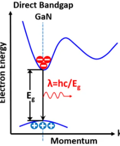
This property is associated with the strength of the chemical bonds between atoms [9]. Therefore, the stronger the bonds, the harder is a jump of an electron from the top of the valence band to the bottom of the conduction band. The energy required to cause this electron movement is Eg= Ec−Ev, where Eg, Ecand Evare the bandgap, the lowest energy of the conduction band and the upper energy level of the valence band, respectively (Figure1.8). WBGS normally have bandgaps about three times or more that of Si. A high bandgap implies lower carrier concentration (ni) and consequently lower leakage current due to its proportional dependence on ni or n2i
1.3. Comparison of semiconductor materials for power applications 7
FIGURE1.8: Simplified energy band diagram of a semiconductor [12].
[13]. Among WBGS, diamond has the widest bandgap (5.45 eV) and consequently, the highest critical electric field. It is followed by GaN (3.45 eV) and SiC (3.26 eV and 3.03 eV for 4H-SiC and 6H-SiC, respectively) with similar bandgaps, but remarkably higher than those of Si (1.12 eV) and GaAs (1.43 eV) [12].
1.3.2 Critical Electric Field
(E
critical)
This characteristic is also related to the chemical bond strength that causes the wider band gap. Hence, WBGS need higher critical electric fields to initiate impact ion-ization, which finally results in an avalanche breakdown. According to Poisson’s equation, the critical electric field and the breakdown voltage can be obtained with the formulas: Ecritical = q NDWD eoer (1.5) VBD= 1 2EcriticalWD = 1 2 q NDWD2 eoer (1.6) where Ecritical, q, ND, WD, eo, and er are the critical electric field, the charge of an electron, the doping density, the width of the drift region, the vacuum permittivity, and the semiconductor relative permittivity, respectively. From the Eq.1.5and 1.6, it can be seen that a 10 times increase in the electric field in conjunction with a 10 times reduction in the depletion width results in a 100 times greater number of electrons, ND, in the drift region. This is the basis that allows the WBGS to outperform Si in power conversion [9]. Moreover, WBGS can reduce their physical size because it is possible to thin the drift region width while obtaining the same breakdown voltage as depicted in Figure1.9.
1.3.3 Electron Mobility
(
µn)
A higher electron mobility allows lower resistivity since it is inversely proportional to the specific RON (resistance times unit area) due to the drift region through the equation:
RON,sp= WD q µnND
FIGURE1.9: Drift region width for each material at different breakdown volt-ages [12].
TABLE1.1: Material properties of Si, SiC, and GaN [9], [12], [14].
Material Ecritical µn er Vsat λ (MV /cm) (cm2/V .s) (×107cm/s) (W /cm.K)
Si 0.3 1350 11.8 1 1.5
4H-SiC 2 720 10 2 4.9
6H-SiC 2.4 370 9.7 2 4.9
GaN 3.3 1500 9 2.5 1.3
By combining the Eq. 1.5and 1.6in 1.7, the following expression is obtained: RON,sp
VBD2 =
4
e0erµnE3critical
(1.8)
Eq.1.8 is known as Baliga figure-of-merit (FOM) and its derivation is based on the assumption that the VBD is due to the critical field [15]. The ratio RON/VBD2 remains fixed once the material is selected because it only depends on the semicon-ductor intrinsic properties rather than the device physical dimensions. Therefore, alternative semiconductors with higher mobility and critical electric field such as WBGS are preferred to obtain an efficient power conversion since they allow a bet-ter trade-off between the breakdown voltage and the ON-resistance.
Figure 1.10illustrates the corresponding theoretical limits (RON,sp versus VBD) by considering the material properties reported in Table1.1, which includes Si and two WBGS (SiC and GaN) for comparison. The WBGS exhibit about three orders of magnitude lower RON,sp compared with Si for a fixed breakdown voltage. For voltage ranges higher than 200 V, Si-based devices dissipate more ON-state power (higher conduction losses) due to their high resistance.
1.4. The Beginning of GaN in power electronics 9
FIGURE1.10: On-resistance versus breakdown voltage for Si, SiC, and GaN [14].
1.3.4 Saturated electron drift velocity
(V
sat)
The drift velocity is directly proportional to the semiconductor capability to switch at high-frequency. WBGS exhibit higher drift velocities compared with Si (see Ta-ble1.1). Therefore, WBGS-based devices are expected to handle very high frequen-cies with smaller recovery current and shorter reverse recovery time [9]. Indeed, important achievements have been reached in the radio frequency (RF) world as reported in the literature by using these materials [16], [17].
1.3.5 Thermal Conductivity
(
λ)
Another advantage of these WBGS is their capability to operate at high tempera-tures, which allow their use in harsh environments and spread their adoption even to aerospace applications [18]. Additionally, some of the WBGS own a high thermal conductivity as in the case of the diamond (22 W/cm.K) and SiC (4.9 W/cm.K ), which is translated into a low junction-to-case thermal resistance Rth−jc. As a result, the heat is easily dissipated out of the device and the device temperature increases slowly.
1.4
The Beginning of GaN in power electronics
Among WBG materials, Gallium Nitride has captured important attention because it fulfills most of the required properties for power applications within the III-V com-pounds such as higher bandgap values, critical field, electron mobility, and satu-ration velocity compared with other semiconductor technologies used for power electronics as previously depicted in Figure1.7. The first RF high electron mobility transistor (HEMT) based on GaN was introduced by Eudyna Corporation in 2004 in Japan. This device was the result of the unusual high electron mobility observed in the region of an aluminum gallium nitride (AlGaN) and GaN heterostructure inter-face [9], [19], [20]. This GaN grown on SiC transistor was able to produce a bench-mark power gain in the multi-gigahertz frequency range.
FIGURE1.11: Increasing trend of the GaN power semiconductor market [21].
Later on, Nitronex Corp fabricated the first RF GaN-based HEMT grown on Si substrates. The journey of GaN in the RF market has been supported by several other companies. However, its adoption outside this market was limited by the fabrication cost as well as the depletion mode operation that will be discussed in detail in the next chapter. It is not until June 2009, that Efficient Power Conversion Corporation (EPC) introduced the first enhancement-mode or normally-OFF GaN FETs grown on Si wafers as a special replacement for power MOSFETs. Since then, many important companies such as Matsushita, Transphorm, Panasonic, RFMD, HRL, among others, have dedicated their manufactured GaN-based transistors to the power semicon-ductor market. As a result, the GaN participation in power applications has highly increased in recent years as illustrated in Figure 1.11
1.5
General limitations for a wide GaN-technology adoption
There are necessary requirements that new semiconductor technology has to fulfill for its wide adoption in power conversion systems. The first one is efficiency, and GaN has demonstrated a complete superiority over Si due to its remarkable char-acteristics, which results in switching devices that allow the design of high-efficient converters with low power loss [22–24].The second one is cost-effectiveness. Although a direct cost comparison among semiconductor technologies is complicated due to all the elements that influence the final cost (epitaxial growth, wafer fabrication, and assembly) [9], we can men-tion that one of the drawbacks of GaN-based devices is the expensive homoepitaxy growth on GaN substrates. Therefore more affordable wafers based on Si have been used to make it more competitive for the voltage rating lower than about 600V range, but this makes the device more vulnerable to defect creation due to the difference in the thermal expansion coefficients and the lattice mismatch between both materials [25], [26]. If the voltage range target is higher, then GaN needs to be grown on SiC and diamond substrates which increase the cost with respect to its Si counterparts.