Investigations of Static And Dynamic
Characteristics of Optically Controlled MOSFET
Saravanan Rajamani
University of Rome “Roma Tre”
This dissertation is submitted in partial fulfillment of the requirements for
the degree of
Doctor of Philosophy in Electronic Engineering
Tutor: Coordinator:
Prof. Lorenzo Colace Prof. Giuseppe Schirripa Spagnolo
ii
Abstract
In recent years, scaling down the dimensions of electronic devices has driven dramatic improvements in the performance of electronic devices. With the increase in device speed and the introduction of exascale computing, the communication bottleneck has become one of the greatest challenge in both short and long distance communications. Traditional metal interconnects are efficient at short distances, but their excessive power dissipation and delay in global lines, makes them unsuitable for the ever-growing bandwidth demand. Currently, Optical interconnects (OIs) provides a solution to the communication bottleneck in long distance communications with their superiority in noise free, low loss, power efficiency and faster data transfer. However, in shorter distances, energy per bit is still higher compared to metal interconnects, due to the large power consumption by the receiver circuits. Since the receiver circuit after the photodetector, consumes most of the power, it is important to minimize the power consumption of the circuits, or if possible, to introduce receiver-less detection. Phototransistors, monolithically integrated to silicon electronics provides a possibility to replace power hungry receiver circuits in short distance (inter chip and intra-chip) communications. Although many phototransistors were reported with III-V compound semiconductors, it is still not easy and cost efficient to integrate them with the silicon photonics. In this context, Ge is becoming increasingly popular in silicon based photonic devices. Due to its strong absorption in the NIR region and its relative ease of integration with Si electronics, it is a promising candidate in fabricating CMOS compatible integrated photoreceivers.
In this work, an optically controlled field effect transistor (OCFET) with Ge as an NIR absorbing gate is designed simulated using ISE-TCAD. The static and dynamic charateristics of the OCFET are studied in terms of Ion/Ioff ratio, responsivity and bandwidth as functions of doping concentrations, channel length, optical power, Ge gate thickness, gate bias and Ge carrier lifetime. A maximum simulated responsivity of 100A/W and the fall time (tfall) as
iii
low as 100ps are obtained. The OCFET in different inverter configurations with parameters like load resistor, W/L ratio of the load MOSFET and CMOS configuration are investigated. A proof of concept of OCFET is investigated by connecting a Ge-on-Si photodiode with the MOSFET gate terminal. The Ge-on-Si photodiode and the trench MOSFET designed and fabricated and OCFET concept is investigated under dark and illuminated conditions.
The final part of this thesis is dedicated to the design, fabrication and characterization of an optical JFET with 4µm and 8µm channel length and Ge thin film of 500nm as the gate. The current-voltage characteristics of the Optical JFET is investigated with open gate and applied gate bias. In the open gate configuration, the device exhibits a signal to noise ratio of 14dB at 0dBm (1mW) optical power compared to 3.7dB at -10dBm (100µW) optical power. The responsivity with floating gate was 5.3A/W, which decreases to 0.13A/W with applied gate bias of -1V.
iv
Acknowledgements
This work would not be possible without the support and encouragement from my advisor, professors, colleagues, friends, and my family.
First of all, I would like to express my deepest gratitude to my advisor, Prof. Lorenzo Colace for his continuous support, encouragement and, most of all, patience. I would also like to thank Prof. Gaetano Assanto, the head of the Nonlinear Optics and OptoElectronics Lab (NooEL), for giving me the opportunity to work in NooEL.
I also want to thank Vito Sorianello (now with CNIT-LNRF), for his advices and discussions on simulations and for his help in fabrication of optical JFET. His remarkable knowledge and insight have always impressed me. I would also like to acknowledge the ST Microelectronics for providing trench MOSFET and Michele for helping in pump-probe experiment setup.
I would like to thank Prof. Giuseppe Schirripa Spagnolo, the coordinator of the doctoral school EDEMOM and Prof. Aldo Rocchegiani, of the research office for their assistance since from the beginning of my PhD.
I would also like to thank all my colleagues at the NooEL: Alessandro, Armando Andrea and Nina. My PhD life would not be so enjoyable without these wonderful people.
Finally, I would like to thank my parents and my sister for their endless love and support made the hard times so much easier.
v
Contents
Abstract ... ii
Acknowledgements ... iv
List of Figures ... vii
List of Tables ... xiii
1 Introduction and Motivation ... 1
1.1 Introduction ... 1
1.1.1 Electrical Interconnects ... 2
1.1.2. Optical Interconnects ... 4
1.1.3. Components of an Optical Interconnect System ... 6
1.2. Receiver End ... 11
1.2.1. Photodetectors ... 11
1.2.2. Receiver Front End ... 21
1.3. Receiver-Less Detection ... 21 1.4. Organization ... 23 2Simulation Tools ... 24 2.1 GENESISe Workbench ... 24 2.1.1. MESH ... 25 2.1.2. DESSIS ... 26 2.1.3. TECPLOT ... 27 2.1.4. INSPECT ... 27
2.2. Models and Parameters ... 27
2.2.1. Parameters ... 28
2.2.2. Physical Models ... 29
3 OCFET Design and Simulations ... 36
3.1. Device Structure ... 36
3.2. Operation ... 38
3.3. Current Voltage Characteristics: ... 41
3.3.1 Doping Dependence ... 44
3.3.2. Gate Voltage Dependence ... 46
vi
3.3.4 Channel Length Dependence ... 50
3.3.5 Gate Thickness Dependence ... 51
3.4. Dynamic Characteristics ... 53
3.4.1 Carrier Lifetime Dependence ... 53
3.4.3. Optical Power and Gate Voltage Dependence ... 56
3.4.4. Doping Dependence ... 58
3.4.5 Channel Length and Gate Thickness Dependence ... 61
3.5 OCFET Inverters ... 66
3.5.1 Inverters with Resistive Load... 67
3.5.2 Inverters with Enhancement Load ... 72
3.5.3 Complementary OCFET Inverters ... 75
4OCFET Proof of Concept ... 81
4.1. Germanium on Silicon Photodiodes ... 81
4.1.1 Device Characterization ... 85
4.1.2. Current-Voltage Characteristics ... 86
4.1.3. Series Resistance ... 89
4.1.4. Responsivity ... 91
4.1.5. Time Resolved Photoresponse ... 93
4.2. Ge-on-Si Photodiode Connected to MOSFET Gate ... 94
5Optical JFET ... 100
5.1 Introduction ... 100
5.2. Device Structure and Operation ... 101
5.3. Characterization ... 102
5.3.1. Ge-Si Heterojunction Photodiode ... 103
5.3.2. I-V Characteristics (Floating Gate) ... 104
5.3.3. Dynamic Characteristics ... 106
5.3.4. I-V Characteristics (With Gate Bias) ... 107
Conclusions ... 111
References ... 113
vii
List of Figures
Figure
1.1 A high performance complex multicore processor...…...2
1.2 A categorization of optical links based on the distance……….………..4
1.3 Bandwidth trend for server and networking I/O………...5
1.4 The components of an optical interconnect system………..7
1.5 Circuit model of an optical receiver………....9
1.6 Absorption coefficient of various semiconductors vs wavelength………10
1.7 A reverse biased pn-junction diode illuminated by photons. The drift and diffusion regions are indicated………..…13
1.8 Schematic illustration of a p-i-n photodiode………..14
1.9 Lattice constants of some frequently used semiconductors versus energy bandgap and cutoff wavelength. Dots refer to elementary materials and curves to compounds, where solid and dashed lines represent direct and indirect bandgap compounds respectively………16
1.10 Schematic of a common phototransistor……….19
1.11 (a) A receiver-less circuit stage with two photodetectors connected in totem pole configuration and (b) A receiver-less circuit stage with a pair of complementary phototransistors connected in totem pole configuration……….……….22
2.1 MESH design flow……….……….25
2.2 Simulation process flow……….……….26
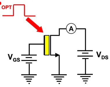
3.1. Schematic 3D representation of Optically controlled FET……….…………...38
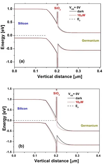
3.2 Energy band diagrams (a) without offset gate bias in dark and 10µW optical input and (b) with offset gate bias of 0.6V in dark and 10 µW optical input ……...…...……...39
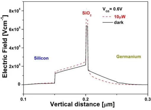
3.3 The electric field across the vertical cross section of the device in dark (solid) and illuminated with 10µW optical input (dashed) with a offset gate bias VG=0.6V ……..40
3.4. Electron (a) and Hole (b) densities at Germanium gate and Si channel regions with gate bias VG=0.6V in dark (solid) and 10µW optical input power………...41
viii
3.5. (a) Drain current vs Gate voltage with a drain voltage VDS=0.5V (b) Drain current vs
Drain voltage of 0.18µm channel length device with the parameters shown in table 3.1. The input optical power is varied from 1nW to 10µW………..…42 3.6 Ion/Ioff ratio and threshold voltage Vth versus oxide thickness tox, at 10μW optical power
at constant (circles) and optimized VG (triangles) for higher ratio……….43
3.7 Ion/Ioff ratio vs Germanium doping concentration with constant Silicon doping of 1017cm-3 for constant gate bias (0.6V) and optimized gate bias for higher ratio. The input optical power is 10µW………..….45 3.8. Ion/Ioff ratio vs symmetric Silicon and Germanium doping concentrations with constant gate bias (0.6V) and optimized VG for maximum Ion/Ioff ratio……….…..46
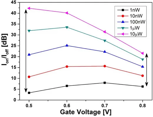
3.9 Drain current vs the gate voltage at optical power varying from 1nW to 10µW. The drain voltage was kept constant at 0.5V……….……….47 3.10 Ion/Ioff ratio vs the gate voltage at optical power varying from 1nW to 10µW……..48 3.11 Drain current (squares) and Responsivity (triangles) depending on the input optical power (Popt). The input gate bias VG=0.6V……….…..49
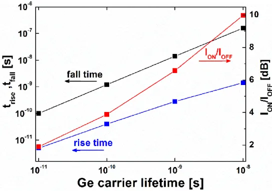
3.12 Responsivity vs channel length (0.09 µm to 0.35 µm) at 10µW input optical power of wavelength 1.55µm. The channel width and drain voltage are kept constant at 1µm and 0.5V respectively……….………..51 3.13. The drain current as a function of Germanium layer thickness at dark conditions and at 1μW and 10μW optical power. The gate bias is constant at 0.6V……….52 3.14 Schematic representation of the simulated circuit for temporal response………….…54 3.15 Transient response of OCFET with normalized drain current vs time as a funcion of carrier lifetime. Actual drain current vs time without normalization is shown in the inset ………...55 3.16 Ion/Ioff ratio, rise time(trise) and fall time (tfall) extracted from the figure 3.15………56
ix
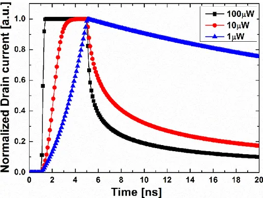
3.17 Normalized drain current vs time as a function of optical power from 1μW to 100 μW with constant gate voltage (VG=0.6V)………..……….57
3.18 Transient response of OCFET with normalized drain current vs time as a function of gate voltage (VG=0.5V, 0.6V and 0.7V). The optical power and carrier lifetime are kept
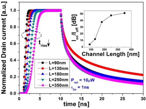
constant at 100μW and 100ps, respectively……….…..58 3.19 Normalized drain current vs time as a function of Silicon and Germanium doping concentrations. In the inset, actual drain current is shown vs time. The doping concentrations are varied between 1016cm-3 and 1017 cm-3 along with the gate bias ….59 3.20 (a) Hole density in the Germanium layer during turn on pulse for 4ns and (b)Hole density during turn off. The samples are taken from 1ns-4ns for turn on and from 5ns to 10ns after the pulse is turned off………60 3.21 Normalized drain current vs time as a function of channel length, with optical power Popt=10µW and carrier lifetime τGe = 1ns……….………….………….…62
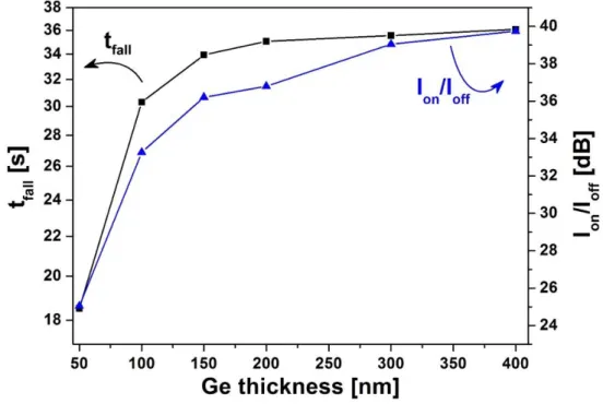
3.22 Drain current vs time, as a function of Germanium layer thickness, with optical input of 10µW, gate bias VG=0.6V and Ge carrier lifetime of 1ns……….………63
3.23 Ion/Ioff ratio and fall time of OCFET extracted from the transient response plot as a function of Ge thickness………64 3.24 Ion/Ioff ratio and fall time of OCFET obtained using different combinations of device parameters……….65 3.25 Voltage transfer characteristics of a resistive load inverter with dark to 10µW optical
power and 100KΩ load resistor……….…67 3.26 KnRL dependence of inverter static characteristics for. Load resistance varied from
50KΩ to 200KΩ in dark and 100µW optical power……….……68 3.27 Inverter output voltage (Vout) vs optical power (upto 10µW) at differrent input voltage
x
3.28 Transient response of resistive load inverter with different load resistors (50KΩ, 100 KΩ and 200 KΩ) for a 4ns optical pulse of 10 μW………70 3.29 Vout vs time of resistive load inverter as a function of Germanium carrier lifetime with optical power of 100µW………71 3.30 Static characteristics of a n-OCFET inverter with an enhancement mode, diode connected mosfet load with W/L ranging from 2.5 to 5……….73 3.31 Voltage transfer characteristics of an active load inverter with (KD/KL) ratio of 5 at
optical power upto 10µW and VDD=Vin=1.5V………..……….74
3.32 Transfer characteristics of an active load inverter for a 4ns optical pulse of 10µW as a function of Vin or VGS (0.55V, 0.6V and 0.65V). The Ge carrier lifetime was kept
constant at 1ns with VDD=1.5V……….……….75
3.33. (a) Circuit schematic of p-OCFET and n-OCFET connected in CMOS configuration and current voltage characteristics of both transistors. The optical input was varied up to 1mW for p-OCFET and 10µW for n-OCFET………..…….76 3.34 Static characteristics of a complementary OCFET inverter as a function of optical power (dark to 100µW) of 1.55µm wavelength and VDD=1V……….……….….77
3.35 Normalized temporal response of a complementary OCFET inverter depending on the 4ns optical pulse of power 10µW to 1mW with Ge carrier lifetime of 1ns….…….…..78 3.36 Temporal response of a complimentary OCFET inverter as a function of input gate voltage with Ge carrier lifetime of 1ns and 10µW to 1mW optical power of wavelength 1.55µm ……….……….79 3.36 Output swing (Vmax/Vmin) vs the rise time of inverters of all configurations showing the tradeoff between speed and sensitivity of the circuits mainly due to the device limitations………..80 4.1 Schematic of a thermal evaporation system……….…..82
xi
4.2. The photodiode geometry. The area of the Ge mesa varies between 60x60 µm2 to
220x220 µm2……….……84
4.3 (a) Schematic representation of Ge on Si photodiode and (b) Image of fabricated photodiodes………..….85 4.4 (a). Dark current density of Ge-on-Si photodiodes as a function of Germanium mesa area
with a thickness of 600nm……….………..…..87 4.4 (b) Experimental values of dark current at -1V as a function of Germanium mesa area. The Ge layer thickness was 600nm……….………..88 4.5. Current density versus reverse bias of a Ge-on-Si photodiode with an area 220µmx220µm as a function of Germanium layer thickness…….………...89 4.6. Series resistance vs the Ge mesa area of 350 nm thickness……….…..90 4.7. Responsivity of Ge-on-Si photodiode as a function of reverse bias for different Germanium layer thickness………...…91 4.8. Fall time vs Ge mesa area of the photodetector as a function of Germanium layer thickness………..…..93 4.9. Schematic representation (a) of the Trench MOSFET and (b) its optical microscope image……….……95 4.10. (a) IDrain-VGS characteristics of the trench MOSFET with VDS=-2V and (b) IDrain-VDS
characteristics of the trench MOSFET with increasing VGS from -2V to -2.8V……...96
4.11. The basic configuration of connecting a photodiode to the MOSFET gate terminal to modify its channel modulation. The simulated monolithic optically controlled field effect transistor is shown in the left………..……….97 4.12. IDrain vs VGate characteristics as a function of optical input power (dark condition and
xii
4.13. Measured drain current vs drain voltage of the circuit as a function of optical input power (1550nm) at VG=2.2V and VD=2V………..99
5.1. Device structure of a p-channel Ge-on-Si Optical-JFET. The light is coupled through a Silicon waveguide with grating coupling between the optical fiber and the waveguide………101 5.2. Current-Voltage characteristics of the Ge-Si heterojunction as a function of optical power………...……103 5.3. Current-Voltage characteristics of the Optical JFET as a function of optical power at floating gate configuration. The optical power was varied from 1µW to 1mW coupled through silicon waveguide via grating coupling to a single mode optical fiber….….104 5.4. Ion/Ioff ratio and responsivity extracted from fig. 5.3, as a function of input optical power at VDS=-3V……… ………..…….105
5.5. Simulated drain current vs time as a function of optical power from 1µW to 100µW. The normalized drain current versus time is shown in the inset……….106 5.6. Drain current vs the gate voltage (VGS) as a function of optical power at a drain voltage
of -2V……….…….….108 5.7. (a) The ratio between the drain current with light and dark conditions at increasing gate bias (VGS=0V to -1V) as a function of optical power (from -30dBm to 0dBm). (b) The
responsivity of the optical JFET at increasing gate bias (from 0V to -1V) at two optical powers (-30dBm and 0dBm). The drain voltage was -2V for both plots……….……109
xiii
List of Tables
Table
2.1. Default parameters for Silicon………...34 2.2. Parameters used for Si and Ge………35 3.1. List of device parameters used in the simulations………..37 3.2. Suggested device parameters for high responsivity and higher bandwidth OCFET…...66 4.1. Device physical parameters of the trench gate MOSFET………..94 5.1. Physical parameters of an Optical JFET………...102
1
Introduction and Motivation
1.1 Introduction
The current age of information technology is in constant need for increased data transfer and data process capability. Nowadays, more advanced electronic systems are required with complex architectures that consist of ultra dense interconnected integrated circuits. Examples of such systems are computer servers and high-performance multiprocessor systems. The computational performance is mainly improved by advances in semiconductor industries.In the early stages of the CMOS technology, the performance of microprocessors was improved by both scaling the number of transistors per area [1] as well as the operating clock frequency [2]. The scaling approach provided a tremendous improvement in performance until the power consumption became an issue. It turned out that by scaling clock frequency, marginal improvement in processing performance was achieved with a significant increase power requirement [3]. As a result, designers employed a parallel computing approach through processors with multiple cores as shown in figure 1.1. In the near future processors are expected to have hundreds or even thousands of cores paving the way to exascale computing [4]. However, with the parallel computing, a number of drawbacks over single CPU based machines emerges. One major issue is the complexity of network interconnects to enable data transfer between the cores. In addition, with the increase in computing power, corresponding improvement in the inter-chip as well as on-chip communication bandwidth is needed.
2
Figure 1.1 A high performance complex multicore processor
1.1.1 Electrical Interconnects
The most widespread interconnect technology used in on-chip and inter-chip interconnect networks is copper based electrical interconnects. The limitations of copper based interconnects (or any electrical) are becoming increasingly obvious as interconnect densities rise to keep pace with device scaling (on-chip) and increased bandwidth (inter-chip/board). The electrical interconnects are reaching their practical limits in terms of loss, dispersion, cross-talk and bandwidth. Because of the resistive loss in electrical lines, considering the case without repeating amplifiers, the bit rate on electrical lines limited by the cross sectional area (A) of the wiring and the length of the wires (L) according to [5];
𝐵 ≤ 𝐵
0𝐴
𝑙
2(1.1)
with B0 as a constant (1015 b/s for high performance strip lines and cables, and ~ 1016 b/s for
small on-chip lines) for the resistive–capacitive lines. In case of on-chip interconnection, the number of connections scales geometrically with the number of cores, since each core needs a point-to-point connection to every other core. Therefore, the density of the network increases, forcing the individual connections to become smaller.
3
Unfortunately, down scaling of the wires used in electrical interconnects increases their resistance since the resistance of a current carrying wire is given by:
= 𝜌
𝑙𝐴 , where ρ
is the resistivity of the wire material, l is the length and A and is the cross sectional area of the wire. At the same time, scaling down of the metal lines as well as the insulating layer between them implies reduction in capacitance. Therefore, the increase in the resistance and decrease in capacitance leaves the RC time constant unchanged [6]. However, as the wire cross sectional dimensions continue to scale downward and circuit speed continues to increase, several factors exacerbate the interconnect latency problem.
Latency is a measure of the time-delay between transmitting and receiving a signal. Electrical signals are limited by the drift velocity of the electrons inside a wire which in turn is dependent on the length of the wire (L), mobility of electrons (µ) in the material and the voltage drop (V) between its ends
.
In order to increase the speed that signals travel through an electrical wire, the voltage and/or the electron mobility must be increased. The fundamental limitation of speed occurs, since higher voltage can damage sensitive electronics and mobility is a function of material properties.In contrast, optical interconnects transfer the signals at the speed of light. This is the upper speed limit for the signals to be propagated and therefore optical interconnections intrinsically have the smallest possible latency.When wire cross-sectional dimensions become smaller than the bulk copper electron’s mean free path length, the separators surrounding a copper interconnect to prevent copper atoms’ migration into the silicon become thicker than the copper interconnect itself. In addition, power dissipation causes increase in the wire temperatures. Finally, the high-speed operation creates a greater current density near the wires’ periphery than in their central region. This so-called “skin effect” leads to greater electromigration effects, when the movement of conductor atoms under the influence of electron bombardments, resulting ultimately in the breaking of conductor lines [7].
The potential of optical interconnections like, a) the density of information that can be sent over relatively short/long distances, b) reducing the skin effect c) speed of transmission depending on the medium and d) the superior immunity to mutual and electromagnetic interference are of considerable interest in choosing optical interconnects over their electrical counterparts.
4
1.1.2. Optical Interconnects
Optical interconnects for microelectronic chips have been studied for a long time [5, 6] several investigation on the comparisons with the electrical interconnects have been made [11-20]. The capacity limitations, losses, cross talk and parasitics along with other disadvantages of electrical wires paved way to the optical interconnects. Already, all long distance communications now switched to optics. For medium distance communication, e.g. LAN, MAN, WAN, optical interconnects is gaining popularity specifically because only optics can support the high data rates required by these applications. At shorter distances (a few meters), primarily in data links, optics is rapidly gaining entry. Research is underway at even shorter distances (board and chip level) to use optics for communication purposes. Figure 1.2 shows the already used and future possibilities of optical interconnections.
Figure 1.2. A categorization of optical links based on the distance.
Given the huge optical interconnect bandwidth needed (figure 1.3), it is unlikely that a single stream of data will meet the growth requirement. Instead, multiplexing techniques like, Time Division Multiplexing (TDM), Spacing Division Multiplexing (SDM) or Wavelength Division Multiplexing (WDM) can be used to tap in the vast available bandwidth of optical fiber [8], [22]. Optical interconnects with these techniques allows, not only higher bandwidth density for global interconnects, but also in board level [9] or chip level interconnects.
5
Figure 1.3. Bandwidth trend for server and networking I/O [10].
In short distance interconnections, the combination with voltage variable gratings, provides selective routing possibilities that can be used for radically different signal processing functions than those currently available. This provides the promise of dramatically increased bandwidth, even while reducing the number of connections necessary to carry all of the information [9].
Using optics provides a very high frequency carrier, at a very short wavelength and a large photon energy. The very high optical carrier frequency eliminates frequency dependent loss in the modulation band, and makes short pulse communication feasible. The short wavelength allows, low loss in waveguides, impedance matching with very low overhead, and wavelength division multiplexing (WDM) [14].
Other advantages of optics include, the density of interconnects. For off-chip or board-to-board interconnects, optics can offer very large densities. Optical devices can be made very small and 1000's of input/outputs (I/O) can be achieved on a chip. Optical interconnects can utilize the third dimension by being able to cross the beams. In free space, a few optical elements can easily handle a large number of beams, providing very high interconnect densities.
6
Most electrical lines are designed for 50Ω impedance, which requires a 50Ω termination to avoid reflections. A lot of power is absorbed in this termination. Optics exploits a potential advantage of impedance transformation that matches the high impedance of small devices to the low impedance associated with electromagnetic propagation [17]. A quarter-wavelength wide index matching material can match the impedance of two dissimilar materials to remove reflections. This is equivalent to the termination in electrical lines; in optics, though, there is virtually no power dissipation in this index matching material. In optics, a beam splitter can be used to tap the optical signal for monitoring, with small or negligible reflections. A similar tap in electrical lines needs to be very well designed to minimize the impedance discontinuities.
With optics, a complete electrical isolation is possible [21], since the voltages on either sides need not be related to each other. This provides noise immunity from one side to the other. With scaling in electronics, the supply currents are increasing and so are resistive drops in dc supply and ground bounce effects. Hence this voltage isolation property of optics may become progressively more important for future generations.
1.1.3. Components of an Optical Interconnect System
In general, an optical interconnect system has three main components: a transmitter, the transmission medium, and a receiver. Binary data from the digital circuits, in the form of voltage levels, is fed to a transmitter driver, which converts these levels into the voltage or current signal required to drive the optical modulator device. The optical modulator converts these electrical signals into the modulation of light beams, which then travel through a propagation medium (optical fiber or waveguide) to destination. At the receiver side, the photodetector converts the optical signal into current, which is then converted into logic level by the receiver system. Figure 1.4 shows the general components of an optical interconnect system.
7
Figure 1.4. The components of an optical interconnect system.
Further, in this chapter, I briefly introduce the different options for optical source, modulators and transmission medium, with the main emphasis on the optical receivers. Since the receiver circuitry directly interfaces with the photodetectors, understanding the operation and characteristics of these devices is essential for an optimum design. However, the main concern of this thesis is on photodetectors, particularly on an optically controlled FET.
Laser Sources: Optical interconnect systems use either off-chip or on-chip laser sources.
One of the main candidate for an optical source is the Vertical Cavity Surface Emitting Lasers (VCSELs) as they have improved significantly in the last few years. Oxide confined VCSELs can achieve very low threshold currents [23]. Sub-mA threshold currents are now easily achieved in VCSELs and optical interconnects with arrays of VCSELs have been already demonstrated [24-25]. But there are many issues like, uniformity of threshold current, wavelength stability and thermal issues that still need to be addressed for using large VCSEL arrays in optical interconnects [26]. Despite the advancements in on-chip sources, Off-chip laser sources are generally preferred due to several problems faced by directly modulating Lasers. Due to non-availability of an efficient and silicon compatible laser and since it is very hard to fabricate large number of lasers on a single chip at reduced cost. Moreover, the complexity of chip design increases significantly since optical source will be a part of the chip’s power and heat budget. Such issues can be mitigated with off-chip light source that individually supply addressable effective source points, located at positions dictated by the interconnect topology, and using modulators and a coupling structure [27].
8
Optical Modulators: Optical modulation is one of the main required functionalities for any
optical interconnect solution. The primary purpose of an optical modulator in a photonic network is to modulate the light source. This modulation can be done either directly or externally, but external modulation offers several advantages over direct modulation: the optical source can be relatively inexpensive and its operation does not need to be compromised by direct modulation, modulation speeds can be higher, and optical isolation and wavelength stabilization need to be performed only once for the entire system. Furthermore, a single light source can feed multiple channels via individual modulators, thus reducing the total power budget of the system [28]. There are various optical modulation techniques through which refractive index or absorption properties of optical medium are varied in accordance with the electrical signal. Current optical modulation techniques are based on Thermo Optic effect, Electro-optic effect, [29] Electro absorption effect and plasma dispersion effect. Another modulation mechanism is the electroabsorption effect involves the change in the absorption coefficient of the material with change in applied electric field. These techniques are more effective in III-IV semiconductors but the most effective method for changing the refractive index of the Silicon is carrier plasma dispersion technique [30]. Several researches are being carried out on optimizing device structures and developing integration techniques for the high speed and low power modulators compatible with current CMOS technologies [28] [31-35].
Optical Channels: Optical channels are similar to electrical links for data transmission. The
two optical channels relevant for long/short distance communications are optical fibers and optical waveguides. These optical channels offer potential performance advantages over electrical channels in terms of loss, cross talk, and both physical interconnect and information density.
Optical fiber based systems provide alignment and routing edibility for chip-to-chip interconnect applications. As shown in Figure 1.3, an optical fiber confines light between a higher index core and a lower index fiber cladding via total internal reflection. Fibers are classified based on their ability to support single or multiple modes. Single-mode fibers with smaller core diameters (typically 8-10µm) only allow one propagating wave, and thus require careful alignment in order to avoid coupling loss. These fibers are optimized for long distance applications such as links between Internet routers spaced up to and exceeding 100km. In addition, Multi-mode fibers with large core diameters (typically 50µm) allow
9
several propagating modes, and therefore provide good coupling characteristics. These fibers are used in short and medium distance applications.
Another means optical communication is employing optical waveguide, mainly in short distance data transfer (like inter chip or intra chip). Similar to optical fibers, waveguides can either support multiple or single optical modes. Usually, to facilitate coupling and reducing assembly costs, multi-mode waveguides are favorable. The waveguide core is surrounded by a cladding layer with smaller refractive index to enable total internal reflection. Due to their large core area, they provide negligible coupling loss. In addition, the modal dispersion is fairly small as they are intended for short range board-level interconnection.
Receivers: The receiver can be divided into two sections, a photodetector that converts light
into electrical signal followed by a receiver circuit that amplifies the analog electrical signal and matches to a digital voltage level. A simplified equivalent circuit model is shown in Figure 1.5. Optical receivers generally determine the overall optical link performance, as their sensitivity sets the maximum data rate and amount of tolerable loss in the channel.
Figure 1.5. Circuit model of an optical receiver
For a better performance, the capacitance of the photodetector and the receiver circuit should be as low as possible. A smaller capacitance device requires fewer gain stages and offers noise immunity. To reduce the capacitance, monolithic detectors can be made in silicon. But silicon has a large absorption depth even at wavelengths near 850 nm (first window of optical communications), much deeper than junction depths in silicon MOS devices. Most photons are absorbed deep inside the substrate causing generated carriers
10
contributing to substrate noise. In order to obtain optical receivers operating at longer wavelengths (typically between 1.3 and 1.6 micrometer), considering compatibility with CMOS technology, a practical solution is to use SiGe or Ge photodetector. Eventhough Ge is an indirect bandgap material (Eg ~ 0.66 eV), it is a strong absorber at the near infrared due to its direct band transition at 0.8 eV, as shown in Fig. 1.6. In addition, the carrier mobility in Ge is higher than in Si, promising faster operation. The smaller bandgap results in somewhat higher thermally generated noise in Ge-based devices. The most attractive feature of Ge is its compatibility with Si processing and low temperature processing capability.
Figure 1.6. Absorption coefficient of various semiconductors vs wavelength
The works on this thesis are focused on using Ge absorbing layer on a conventional MOSFET at 1550nm to achieve receiverless detection. However, a brief introduction is given on receiving amplifiers and different types of photodetectors (photodiodes and phototransistors).
11
1.2. Receiver End
1.2.1. Photodetectors
In general, the semiconductor photodiode detector is a p-n junction structure that is also based on the internal photoeffect. Photons absorbed in the depletion layer generate electrons and holes which are separated by the local electric field. The two carriers drift in opposite directions. Such a transport process induces an electric current in the external circuit [36]. Some photodetectors (Avalanche photodetectors) incorporate internal gain mechanisms so that the photoelectron current can be physically amplified within the detector and thus make the signal more easily detectable. The main figures of merit of a photodetector are, responsivity (R), quantum efficiency (η) and response time.
The quantum efficiency is an important parameter representing the capability of the photodetector to convert a photon in an electron-hole pair; if η is 1, every single photon generates a carrier pair. If we consider a photoconductor of thickness d, neglecting reflections at the interface, the quantum efficiency can be expressed in function of the absorption coefficient (α) as:
𝜂 = 𝜂
𝑐(1 − 𝑒
−𝛼𝑑) (1.2)
where ηc is the collection efficiency, i.e. the percentage of carriers generated and
contributing to the photocurrent, and generally can be considered close to 1. The quantum efficiency is a function of wavelength, principally because the absorption coefficient (α) depends on wavelength (as shown in fig. 1.6).
The responsivity of a photodetector indicates how efficiently light is converted in to photocurrent and, is given by, the ratio between the photocurrent Iph flowing in the
photodetector divided by the incident optical power Pin:
𝑅 =
𝐼
𝑝ℎ𝑃
𝑖𝑛(1.3)
The responsivity decreases with large optical power. This condition, which is called detector saturation, limits the detector’s linear dynamic range, which is the range over which it responds linearly with the incident optical power.
12
1.2.1.1. Junction Photodiodes
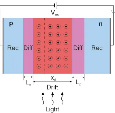
A simple form of a junction photodiode is a p-n junction detector, whose reverse current increases when photon are absorbed. Consider a reverse biased pn-junction as shown in fig. 1.7. Photons are absorbed all over the diode with absorption coefficient α. Whenever a photon is absorbed, an electron-hole pair is generated, but only where an electric field is present the charge carriers can be transported in a particular direction. Since a pn junction can support an electric field only in the space charge region, photocarriers are desirably generated in this region. The photocurrent is associated with two fundamental mechanisms: drift and diffusion. The main contribution is the drift current associated to the carriers generated in the space-charge region. Here the generated electrons and holes are swept and transported by the electric field to the neutral regions where they recombine with majority carriers from the electrodes. The reverse bias to the diode helps to increase both the absorption efficiency and the collection efficiency. Therefore, the photocurrent in the drift regime increases with reverse voltage. Photons absorbed in the neutral regions also generate photocarriers that partially contribute to the photocurrent. In fact, the absence of electric field allows the generated carriers to recombine without affecting the charge neutrality. Only the photocarriers generated in the proximity of the space charge region (about one diffusion length) can contribute to the photocurrent.This current represents the diffusion contribution to the photocurrent and, as it is not affected by the electric field, it is constant with the reverse bias.
13
Figure 1.7. A reverse biased pn-junction diode illuminated by photons. The drift and diffusion regions are indicated.
Although drift and diffusion currents contribute to the photocurrent, it is important to minimize the diffusion current for a high performance photodetector. The transit time of the carriers drifting across the depletion region play a role in the response time of the detectors. In photodiodes there is an additional contribution to the response time arising from diffusion. Carriers generated outside the depletion layer, but sufficiently close to it, take time to diffuse into it. This is a relatively slow process in comparison with drift mechanism. The typical times allowed for this process are the carrier lifetimes (τp for electrons in the p region and τn
for holes in the n region). This effect of diffusion time can be decreased by using a p-i-n diode.
As a detector, a p-i-n photodiode has a number of advantages over a p-n photodiode. A p-i-n diode is a p-n junction with an intrinsic (undoped or lightly doped) layer sandwiched between the p and n layers. Figure 1.8 shows the schematic of a p-i-n photodiode. This structure serves to extend the width of the region supporting an electric field, in effect widening the depletion layer. This electric field drives the electrons and holes generated by the incident photons in the intrinsic region to the n and p terminals, respectively. The result
14
is a current proportional to the number of photons absorbed per second, which is called photocurrent. In the p-i-n diode, a reverse-bias across the diode ensures a strong field in the intrinsic region and a very small current in the absence of light, which is referred to as dark current.
Figure 1.8. Schematic illustration of a p-i-n photodiode
Photodiodes with the p-i-n structure offer the following advantages,
Increasing the width of the depletion layer (where the generated carriers can be transported by drift) increases the volume available for capturing light.
Increasing the width of the depletion layer reduces the junction capacitance and thereby the RC time constant. On the other hand, the transit time increases with depletion layer width.
Reducing the ratio between the diffusion length and the drift length of the device results in a greater proportion of the generated current being carried by the drift mechanism.
Furthermore, the depletion-layer width W in a p-i-n diode does not vary significantly with bias voltage but is essentially fixed by the thickness of the intrinsic region.
T
he capacitance has a simpler expression, mainly dependent on the i -layer width w,𝐶
𝑗=
𝜀
0𝜀
𝑟15
The series resistance Rs depends on the resistance of the neutral regions and the contact resistance of the metal/semiconductor contacts. Since at increasing reverse biases the depletion region widens, the contribution of the neutral regions becomes less important at higher reverse voltages, approaching zero when the punch through condition is reached. Typical values of Rs are of the order of a few Ohms. The p-i-n photodiodes exhibit better performance with respect to the p-n junction diodes. In fact, in p-n photodetectors it is very important to properly tune the doping levels to achieve a better trade-off between neutral region resistivity and depletion region width. In p-i-n photodiodes, this is less crucial because it is possible to act on p and n doping without affecting the depletion region, which is restricted to the i-layer width.
The two serious limitations on the speed of a p-i-n photodiode are, the transit time through the depletion region and the charging/discharging time of the diode capacitance [37]. The other limitations like diffusion time and charge trapping can be minimized by detector design. The transit time is directly related to the depletion width (L) and it is governed by the speed of slower carriers (holes) generated at the opposite end of the depletion region. So the transit time can be approximated as, 𝜏𝑇𝑟 = 𝐿 𝑣⁄ ℎ, where vh is the hole velocity. This
suggests that a high speed can be achieved with thinner intrinsic layer, but at the expense of increased capacitance. Further the efficiency of a p-i-n photodetector with a thin absorbing layer is proportional to the thickness as 𝜂 ∝ 𝛼𝐿, where α is the absorption coefficient. So the bandwidth efficiency product of a p-i-n detector limited by its intrinsic material properties.
1.2.1.2. Heterojunction Photodiodes
Heterojunction photodetectors are photodiodes with different materials in the junction, i.e. with unequal bandgap energies (Eg). The heterojunctions allows more design flexibility
and better performance. For example, consider a normal incidence p-n detector in which the top layer has Eg1 > Eg2. Photons with energy Eg1 > hν > Eg2 can pass through the top layer
without absorption while are absorbed in the bottom material minimising the diffusion photocurrent from the top neutral region and improving the temporal response. Another important advantage is the possibility to realize photodetectors at certain wavelengths with the substrate being transparent in that spectrum. In realizing a heterojunction detectors, the main method is to grow thin films on a bulk substrate. Even though it could be possible to
16
deposit any material on any semiconductor, a successful heteroepitaxy (in terms of crystal quality) is attained if two materials have the similar crystal structure and lattice parameters. Fig. 1.9 shows the lattice constants of the most relevant semiconductors (used in different combinations) used for photodetection versus bandgap energy and cutoff wavelength.
Figure 1.9. Lattice constants of some frequently used semiconductors versus energy bandgap and cutoff wavelength. Dots refer to elementary materials and curves to compounds, where solid and dashed lines represent direct and indirect bandgap compounds respectively. Considering the fact, that the electric and optical properties of the heterostructure directly depends on the crystalline quality, it is necessary to choose the less mismatched material-substrate combination to obtain the least defected heteroepitaxial layer.
As the optical communication window is in the range of 1.3 to 1.6 µm (C-band), photodetectors in this particular range of wavelengths are discussed. It is evident from figure 1.6, ternary and quaternary compounds based on III-V semiconductors such as Gallium Arsenide (GaAs), Indium Arsenide (InAs) and Indium Phosphide (InP) are better suitable materials for this spectral range. Alloy such as InGaAsP [39] allow extreme flexibility with variable cutoff wavelengths in the range 1 µm to 1.8 µm depending on composition. For
17
third-window applications, the best solution is represented by lattice matched InGaAs on InP heterojunctions with cutoff wavelengths at 1.65 µm [40]. III-V photodetectors are widely used in near-infra red detection thanks to their superior performance in terms of sensitivity and speed. Unfortunately, this superiority comes with a drawback: the lattice mismatch prevents the deposition of III-V thin films on Si substrates; therefore, it is necessary to use the more expensive InP substrates. This incompatibility prevents the monolithic integration of III-V devices with standard Si electronics. Thus, signal processing requires either the monolithic integration of detectors on expensive III-V electronics, or the hybrid integration of III-V devices on Si electronics by means of sophisticated techniques like for example, wafer bonding. There are several researches being carried out on hybrid opto-electronic integrated circuits (OEIC). However, monolithic integration on Si would sensibly reduce costs of NIR optoelectronics taking advantage of the well-established Si CMOS technology [41].
As Si is transparent to wavelengths longer than 1.1 µm (Eg = 1.11 eV), several
solutions have been investigated to integrate NIR absorbing semiconductors with Si in order to realize integrated Si-based NIR detectors. Germanium has been recognized as a main candidate for Si based NIR photodetectors [42, 43]. Thanks to its lower bandgap (0.66 eV) corresponding to an absorption cutoff wavelength (𝜆𝑐 = ℎ𝑐
𝐸𝑔) up to 1.8 µm (Fig. 1.8).
Germanium, a group IV material the same as Si, avoids the cross contamination issue. Its direct bandgap of 0.8 eV is only 140meV above the dominant indirect bandgap. As a result, Ge offers much higher optical absorption in 1.3µm-1.55 μm wavelength range, thus making Ge-based photodetectors promising candidates for Si photonics integration. However, the 4% lattice mismatch between Ge and Si places challenging obstacle towards monolithic integration of high-quality low dislocation density devices through Ge on Si heteroepitaxy. Nevertheless, single crystalline device grade Ge films have been demonstrated by many groups with high performance Ge photodetectors. At the starting stage of Ge-on-Si photodetector development for Si photonics applications, normal incidence Ge photodetectors were first fabricated and comprehensively studied. In 2000 Colace et.al. [44] demonstrated a Ge-on-Si heterojunction photodetector fabricated by UHV-CVD with responsivities of 550mA/W at 1.32 µm and 250 mA/W at 1.55 µm and time responses shorter than 850 ps. Later, Famà et.al, demonstrated a p-i-n photodetector [45], with 0.89 A/W and
18
0.75 A/W at 1.32 µm and 1.55 µm respectively, and a response time of <200ps. Dosunmu et.al, fabricated a resonant cavity enhanced Ge- Schottky photodetectors with bandwidth up to 12 GHz at 1540nm [46]. Jutzi et al. [47] fabricated a normal incidence Ge-on-Si photodetectors by molecular beam epitaxy (MBE) with responsivity as high as 0.73 A/W at 1.55 µm and a remarkable bandwidth of 39 GHz. Among the reported NIR photodetectors, Klinger et al. [48] reported the highest bandwidth of 49 GHz for Ge-based photodetectors. The Ge p-i-n photodiode was fabricated in Ge grown by MBE two-step Ge growth. The reported responsivity at 1.55 µm is ~0.05 A/W limited by small device footprint and relatively large density of defects in the Ge layer.
In order to reach a higher responsivity, a thick Ge absorption layer is needed. The highest reported value at 1.55 µm wavelength for normal incidence NIR photodetector is 0.75 A/W [45].As the Ge growth technique becomes mature and the characteristics of Ge-Si devices have been studied in detail, research has been gradually redirected to the integration of Ge photodetectors on Si waveguides to decouple the trade-off between bandwidth and efficiency. To date, a number waveguided Ge photodetectors have been demonstrated [49-56]. Both PIN and MSM structures are reported in these waveguide photodetectors with comparable performance and high speeds of around 40 GBit/s. A waveguided photodetector with the responsivity approaching the theoretical limits were demostrated by Yin et al. [51]. They demonstrated Ge-on-Si n-i-p waveguide photodetectors with responsivity as high as 1.16 A/W at 1.55 µm, operating at 30 GHz.
For a photodetector to be used in Si photonics integrated circuits, a next level pre-amplifier is necessary to further transform the current signal into a voltage signal for further processing. Avalanche photodetectors offers much lower signal-to-noise ratio compared to PIN or MSM structures. Ge-on-Si avalanche photodetectors were also investigated with remarkable results [52,57,58]. A Ge based APD was first reported by, Kang et al [57]. The reported Ge-on-Si avalanche photodetectors operating at 1.3 µm, with an excellent gain-bandwidth product of 340 GHz and a sensitivity as good as -28 dBm at 10 Gb/s.
19
1.2.1.3. Phototransistors
Phototransistors are another form of photodetectors, which have internal gain added with responsivity, besides APDs.Combining a detector and a transistor into a single device is an excellent approach towards realizing the receiver-less detection (Section 1.3) which is desired in chip-level optical interconnects. Such a device should be easily integrated into the existing process technologies and can be readily scaled down to obtain extremely low device capacitance. The additional gain mechanism in phototransistors, also helps to relieve input light requirement which would otherwise be quite stringent with only primary photoresponsivity. The first demonstration of a phototransistor was carried out by Bell Labs [59-61]. Figure 1.10 shows a common phototransistor, it differs from a standard bipolar transistor by omitting the base contact, and have a much larger base and collector areas compared to the emitter.
Figure 1.10. Schematic of a common phototransistor
The performance of the phototransistor later improved (high current amplification factor) using heterojunctions, with emitter being wide bandgap than the base [62]. The homojunction transistors requires a lightly doped base and a heavily doped emitter for efficient injection from the emitter to the base, whereas the barrier at emitter-base heterojunction of the HPTs (Heterojunction Phototransistors) alone can prevent reverse
20
injection from the base. Hence, a heavily doped base can be used to reduce the base resistance and a lightly-doped emitter can be utilized to decrease the base emitter capacitance. Further better characteristics were achieved by taking advantage of the avalanche multiplication in the base-collector junction of the phototransistor to enhance current amplification [63, 64].
Despite the improvements in performance, the gain-bandwidth products achieved from the phototransistors were limited and not exceeding that of APDs. In addition, heterojunction phototransistors are considered too costly to be commercially feasible. Hence, the research on phototransistors was then taken over by other photodetector technologies like APDs. However, since the current research trends in optical interconnects requires integrated photodetectors, there is now a revival of research interests on phototransistors. Furthermore, the improved technologies of growing germanium on silicon wafers permits the heterojunction phototransistors to be built on Ge/Si stacks and thus solving the problems with compound semiconductor (III-V) technologies which lack the vital cost-effective integration capacity with advanced silicon VLSI technology.
Historically, the bipolar structures attracted most of the interest in the research on phototransistors. But from late 80’s, a great deal of interest was shown towards the photosensitivity of field-effect transistors (FET). The photosensitive FET covers a class of FETs including JFETs, MESFETs, and MOSFETs that combine high-impedance amplifiers with built-in photodetectors [65-74].The advantages of FET photo-transistors that combine high-impedance amplifiers with built-in photodetectors are believed to have very fast response and high optical gain. A first demonstration FET photodetector was done by Baack et al with GaAs MESFET. They abserved a rise time of 46ns compared to 74ns for a APD [65].
The FET-photodetectors based on compound semiconductor technologies lacks the vital cost-effective integration capacity with advanced Si VLSI technology. Germanium being a group IV semiconductor provides advantages in cost effective integration with silicon and avoiding cross contamination issues. In this work, I study an optically controlled field effect transistor replacing the MOSFET gate with Ge as an absorbing layer.
21
1.2.2. Receiver Front End
The task of an optical receiver front-end is to convert the current from the photodiode into a voltage and amplify the signals in order to be accepted by CMOS logic stages (fig 1.4). A transimpedance amplifier (TIA) is mainly used instead of a simple resistor. The strong trade-off between the bandwidth and SNR of a front-end with a simple resistor makes it impractical for many applications. The effective input resistance of the front-end can be reduced significantly by adding an active component to the design, resulting in a transimpedance architecture. A transimpedance amplifier (TIA) is an analog front-end with reduced input impedance and a relatively high current-to-voltage gain.
The transimpedance amplifier stage, consumes most of the power, and it is typically followed by several buffer/amplifier stages. In order to minimize the power consumption at the transimpedance amplifier stage, we need to minimize the output capacitance of the photodetector. However, if the output capacitance of the photodetector is still too high, the power consumption of the receiver circuit can easily exceed the power requirement of optical interconnects. Integrated front-ends have been demonstrated to reduce the power consumption and area of the front-end by eliminating the need for TIAs [124]. The main advantage of this technique is that it mainly employs digital circuitry that allows for achieving considerable power saving by scaling to advance technology nodes. Another advantage associated with this technique is that, it reduces receiver sensitivity to common-mode interferences
1.3. Receiver-Less Detection
A receiver-less optical receiver circuit (Fig.1.11-a), which includes a pair of photodetectors, has been proposed to eliminate the power inefficient transimpedance amplifier stage. The top diode, connected to the supply, injects a rising edge. The bottom diode, connected to ground, resets the voltage back to its initial ground state. Both diodes limit the swing of the node in the middle. By alternating pulses on both detectors, a precise square wave can be injected to the next stage. If the input optical power is high enough to charge and discharge the input node close to Vdd and GND in less than a bit-time, a simple
inverter can recover a full swing voltage and resolve the received data. The required input modulation optical power for a full voltage swing is proportional to the photodiode responsivity. The minimum optical power is proportional to the total capacitance, requiring
22
very small photodiode capacitances as well as the small voltage buffer that follows it. However, this configuration requires two optical signals (direct and inverted), precisely separated in time, arrive at the detectors.
Fig 1.11. (a) A receiver-less circuit stage with two photodetectors connected in totem pole configuration [75] and (b) A receiver-less circuit stage with a pair of complementary phototransistors connected in totem pole configuration.
A pair of complementary phototransistors can be connected in totem-pole configurations (fig. 1.11-b), replacing the photodiodes. Phototransistors are a unique optical detector in which light detection (photodiodes) and electrical signal amplification
23
(transistors) are combined in a single device and thus have minor issues of noise increments, high voltages and high cost.
An important example is discussed in this thesis, that is the simulation and investigation of Ge gate MOSFETs on Silicon substrates, studying the above configuration, with complementary OCFETs (Optically Controlled FETs).
1.4. Organization
The following Chapter 2 provides a background information on the simulation software (ISE-TCAD) used for the investigation of the characteristics of optically controlled FET. This chapter also explains the physical models used in this study along with the changes in Ge material parameters. The simulation of the OCFET structure and its static and dynamic characteristics are described in chapter 3. In this chapter, inverter configurations like resistive load and active load inverters using OCFET as driver transistor and as a load transistor as well in the CMOS configuration are investigated. A set of parameters are identified for both high responsivity (Ion/Ioff ratio) and high speed operations of the OCFET. Chapter 3 also provides the design and simulation of an Optical-JFET and its characteristics.
Chapter 4, describes the fabrication and characterization of a Ge-on-Si heterojunction photodiode and a Trench-MOSFET. The OCFET concept is verified by connecting the Ge photodetector to the trench-MOSFET gate and its current-voltage characteristics are investigated in this chapter. Chapter 5, describe the design and the fabrication of a Ge gate heterojunction FET (JFET). The Current-Voltage characteristics of this Optical-JFET are investigated in this chapter.
24
2
Simulation Tools
This chapter gives an overview of tools of ISE-TCAD, which are used to generate and simulate an optically controlled FET (OCFET). Technology Computer Aided Design is a software dedicated to the design and simulation of semiconductor devices for various applications. ISE-TCAD software package provides a selection of tools to solve fundamental, physical partial differential equations, such as diffusion and transport equations, to model the structural properties and electrical behavior of a semiconductor device.
2.1 GENESISe Workbench
GENESISe is the front-end graphical user interface framework for managing projects, simulation tools and analyzing simulation results [76]. It provides a flexible environment to perform multiple simulations on a single device by parameterizing the structural and physical properties to study the device characteristic variations depending on the values of some parameters in a single project as different experiments. It automatically passes the output file of one tool (for eg. MESH) to the next tool (for eg. DESSIS) in the queue removing the need of a manual control by the user.
25 The ISE-TCAD package includes following tools,
DESSIS DIOS LIGAMENT MDRAW MESH PROSIT EMLAB SOLIDIS ISEXTRACT OPTIK INSPECT TECPLOT
2.1.1. MESH
The mesh generator tool is used to define 1D-3D structures with boundary description and complex grid of the device to be studied. In the boundary file (msh.bnd), the device is defined as a list of geometrical figures that defines the structure. After all the bulk materials are in place, contacts are defined as 1D structure to the surfaces or defined regions. These are used to apply external voltage and calculate the current flow through them.
Figure 2.1. MESH design flow
The MESH command file (msh.cmd) contains informations about type, level and distribution of doping for each region as well as the refinement specifications of particular part of the grid. Beside the constant doping concentration in the bulk, doping profiles can be set with the shape of a gaussian or an error function. Before the mesh is finally generated, regions of interest can be defined, in which the mesh points are narrowed down, e.g. in regions with a large change in the doping concentration. The output contains two files namely msh.grd and msh.dat containing the structure of the grid generated and doping information for all grid points respectively. The device structure, generated grids and refinements can be viewed in TECPLOT.
26
2.1.2. DESSIS
The DESSIS tool provides numerical simulation of the electrical behavior of a single semiconductor device or several devices in a circuit. Numerous physical device models provides a close approximation of semiconductor devices to the real behavior of devices.
These features of dessis can be summarized as [77]:
A general support for different possible device geometries (1D, 2D, 3D, and 2D cylindrical).
An extensive set of models for device physics (drift-diffusion, thermodynamic, and hydrodynamic models) and effects in semiconductor devices (optical generation, interface physics, and traps).
A broad set of non-linear solvers.
A mixed mode support of electrothermal netlists with mesh-based device models and Spice circuit models
Possibility of analyzing DC, AC, noise and transient responses.
The MESH output files (msh.dat and msh.grd) along with dessis parameter file (.par) and command file (des.cmd) forms the input of the DESSIS tool. The physical models describing carrier distribution and conduction mechanisms are solved for numerical outputs (voltage, current and charges) of the device. The processing technology and device simulation can be described as schematically shown in fig.2.2,
27
2.1.3. TECPLOT
Tecplot is a software program dedicated to graphical visualization of simulated 2D and 3D structures and the results of the simulations. It can also export physical quantities, mentioned in the plot section of the dessis file at a cross section of the device. This extracted data in .plt format is an input file for Inspect.
2.1.4. INSPECT
INSPECT is a tool for viewing and analysing graphs of currents, voltages and charges on the electrodes of the device or even at specific points on the grid. It supports DF-ISE and XGRAPH input data formats and export data in either formats. The input files be (.plt) generated by dessis or data of specific parts of the device extracted from Tecplot either in the form of .plt or .xy.
2.2. Models and Parameters
ISE-TCAD uses a set of default parameters for each material, which can be modified either in the physics section of dessis command program or in the material parameter file (.par). Usually these parameter files are available as material.par in the default location. The path of the parameter file can be changed to current project folder by specifying “Parameter = Material.par”, in the file section of the dessis program. In this case any parameter for each material used can be modified by the user. Since this work is focused on germanium (Ge) with 1.55µm wavelength optical source, other materials like Silicon, and SiO2 are left
unchanged. The file section of the dessis.cmd is modified as below to redirect the germanium parameter file path to current directory.
File {
Grid = "@grid@" Doping = "@doping@"
Parameter = "Germanium.par" }
28
2.2.1. Parameters
Permittivity ε
r:
The default value for Germanium in ISE-TCAD is 15.8 [77]. Other closervalue for εr is 16.0 [78] and [79]. In other university databases like Ioffe Institute [80] and in
[81] εr =16.2 is found. The default value of εr is used in the simulations. The default values
of permitivity for Silicon (11.7) and SiO2 (3.9) are used.
Refractive Index:
The refractive index can be defined as, A constant in dessis input file A dependence on the mole fraction and temperature in dessis parameter file
A table based optical property that depends on photon energy (eV) can be entered in the DESSIS parameter file.
In this study, the third step is followed to define refractive index (n) along with the extinction coefficient (κ) as a function of wavelength (λ).
The absorption coefficient is computed from the table format of Optik database (TableODB) from the real refractive index (n), extinction coefficient (κ) and wavelength (λ) by,
𝛼(𝜆) =
4𝜋𝜅
𝜆
(2.1)
The TableODB is defined as follows for absorption coefficient =1000 cm-1[82] TableODB
{ *Table format of the Optik DataBase *WAVELEN n k #absorption coefficient = 1000 cm^-1 1.54 4.3 0.0123; 1.55 4.3 0.0123; 1.56 4.3 0.0123; 1.57 4.3 0.0123; }
29
Thermal Conductivity:
Temperature dependent thermal conductivity is defined by,Kappa
{ * Lattice thermal conductivity * Formula = 1:
* kappa() = kappa + kappa_b * T + kappa_c * T^2 kappa = 1.66667 # [W/(K cm)]
kappa_b = 0.0000e+00 # [W/(K^2 cm)] kappa_c = 0.0000e+00 # [W/(K^3 cm)] }
The default value in ISE is 1.6667 W.K-1.cm-1 which is for 125°K. In this study kappa=0.60 W. K-1.cm-1 is used for 300°K [83]. Since the temperature dependence is not studied extensively in this project, this model is rarely used.
Bandgap E
gand Electron Affinity χ
0:
ISE-TCAD uses Eg = 0.74 eV (0°K)as the defaultvalue. This can be found also in several books on semiconductors, e.g. [78]. The default value from Synopsys Sentaurus as well as the values from the semiconductor books is χ0 =
4.0 eV [78]. Default values are used for both parameters.
Recombination:
The doping dependence of the Shockley–Read–Hall lifetimes is modeled in DESSIS with the Scharfetter relation:𝜏
𝑑𝑜𝑝(𝑁
𝑖) = 𝜏
𝑚𝑖𝑛+
𝜏
𝑚𝑎𝑥− 𝜏
𝑚𝑖𝑛1 + (
𝑁
𝑁
𝑖𝑟𝑒𝑓
)
𝛾
(2.2)
The Scharfetter relation is used when Doping Dependence is specified in SRH recombination. In this study, several values of τmax and τmin are used to vary the
recombination time of the carriers.
2.2.2. Physical Models
In ISE-TCAD a number of physical models are provided to describe the device physics as closely as possible to the real device. These models deal with the behavior of the carrier
![Fig 1.11. (a) A receiver-less circuit stage with two photodetectors connected in totem pole configuration [75] and (b) A receiver-less circuit stage with a pair of complementary phototransistors connected in totem pole configuration](https://thumb-eu.123doks.com/thumbv2/123dokorg/2836446.4829/35.892.119.782.207.885/receiver-photodetectors-connected-configuration-complementary-phototransistors-connected-configuration.webp)