Università degli Studi di Ferrara
DOTTORATO DI RICERCA IN
SCIENZE DELL’INGEGNERIA
XXI CICLO
COORDINATORE Prof. Stefano Trillo
M
ODELING AND
R
ELIABILITY OF
I
NNOVATIVE
F
LASH
M
EMORIES
Settore Scientifico Disciplinare ING-INF/01
Dottorando Tutore
Dott. ANDREA PADOVANI Prof. ANDREA
CHIMENTON
Co-Tutore
Prof. LUCA LARCHER
Acknowledgments
hese three years of work toward my Ph.D graduation have been a wonderful and intense period, during which I met, discussed with and had the pleasure to work with a lot of people from both academia and semiconductor industry. I am truly grateful to all of them: they all contributed to my personal and professional growth.
Above all, I am in debt with my Tutor, Prof. Andrea Chimenton, Università di Ferrara, and my co-Tutor, Prof. Luca Larcher, Università di Modena e Reggio Emilia. They have been great minds to work with, great teachers and also good friends.
I’m also really grateful to Prof. Paolo Pavan, Università di Modena e Reggio Emilia for his constant support. He has been fundamental for my personal and professional growth.
These three years would have not been the same without my true friend and colleague Riccardo Brama: sharing the office in Reggio Emilia with you was one of the best things of these three years. We also shared the experience of our first performance as speakers during the 2006 IRPS: that was definitely a bonding experience!
The last, but way more important thanks go to my family, Elena and Matteo, for being supportive and patient: if I reached what I have is only because of you.
“We have a habit in writing articles published in scientific journals to make the work as finished as possible, to cover all the tracks, to not worry about the blind alleys or to describe how you had the wrong idea first, and so on. So there isn't any place to publish, in a dignified manner, what you actually did in order to get to do the work”
Table of Contents
Acknowledgments
………. iTable of Contents
………. ivList of Acronyms
..……… viiList of Figures
………. ixList of Tables
………xiiiCHAPTER ONE
Introduction
1CHAPTER TWO
Flash Memories: Past, Present and Future
3 II.1 Applications ……… 5 II.2 Fundamentals of NVMs ……… 6 II.3 The Floating Gate device ……… 6II.3.1 Charge injection mechanisms ……… 9
II.3.2 Flash architectures ……… 11
II.3.3 Scaling limits of FG devices ……… 13
II.4 Innovative NVM devices ……… 15
II.4.1 Band-Gap engineered devices ……… 17
II.4.2 Charge-Trapping devices ……… 19
CHAPTER THREE
Statistical Monte Carlo Simulator
22
III.1 Simulation model ……… 23
III.2 PTAT conduction model ……… 25
III.3 Simulation results ……… 26
III.4 JLEAK statistical simulations ……… 30
III.5 Chapter Summary ……… 33
CHAPTER FOUR
I
D-V
GSBased Tools to Profile Charge
Distributions on NROM Memory Devices
34 IV.1 Devices and experiments ……… 35IV.2 Device simulations ……… 37
IV.3 Temperature monitor ……… 39
IV.4 Subthreshold slope monitor ……… 41
IV.5 Charge profiling tools discussion and comparison ……… 43
IV.5.1 Programmed cells ……… 43
IV.5.2 Erased cells ……… 46
IV.5.3 Comparison with other charge profiling methods ……… 49
IV.6 Chapter Summary ……… 50
CHAPTER FIVE
Hole Distributions in Erased NROM Devices:
Profiling Method and Effects on Reliability
51 V.1 Experiments ……… 52V.2 Hole charge profiling ……… 53
V.3 Nitride charge evolution with cycling ……… 57
V.4 Correlation to memory retention: erase VTR drift ……… 60
V.5 Chapter Summary ……… 63
CHAPTER SIX
Modeling TANOS Memory Program Transients
to Investigate Charge Trapping Dynamics
64
VI.1 Physics-based model ……… 65
VI.2 Electron trapping dynamics ……… 68
VI.3 Evolution of the trapped charge ……… 70
VI.4 Chapter Summary ……… 71
CHAPTER SEVEN
Conclusions
73Bibliography
……… 75Author’s Publications
……… 82List of Acronyms
BGE – Band-Gap Engineered BTBT – Band-To-Band-Tunneling CB – Conduction Band
CBO – Conduction Band Offset CG – Control Gate
CHE – Channel Hot Electron
CHEI – Channel Hot Electron Injection
CHISEL – CHannel Initiated Secondary ELectrons CMOS – Complementary Metal Oxide Semiconductor CP – Charge-Pumping
CT – Charge Trapping DD – Drift-Diffusion DT – Direct Tunneling DV – Depletion Verify
ECC – Error Code Correction ECU – Engine Control Unit
EOT – Equivalent Oxide Thickness EV – Erase Verify
FE – Full-Erased FG – Floating Gate FN – Fowler-Nordheim
FeRAM – Ferroelectric RAMs GCR – Gate Coupling Ratio
GIDL – Gate-Induced Drain Leakage GPS – Global Positioning System HDD – Hard-Disk Drives
HE – Half-Erased
HHI – Hot Hole Injection IPD – Inter-Poly Dielectric MC – Monte Carlo
MLC – Multi-Level Cell
MRAM – Magnetoresistive RAM MTJ – Magnetic Tunnel Junction NVM – Non-Volatile Memory MC – Monte Carlo
ONO – Oxide-Nitride-Oxide OP – Over Programming PC – Personal Computer PCM – Phase Change Memory PDA – Personal Digital Assistant PF – Poole Frenkel
PTAT – Phonon Trap-Assisted Tunneling PV – Program Verify
RL – Read Level
SILC – Stress-Induced Leakage Current SRH – Shockley-Read-Hall
SSD – Solid-State Drive
SSM – Subthreshold Slope Monitor TAT – Trap Assisted-Tunneling TBT – Trap-to-Band Tunneling TE – Thermal Emission
TM – Temperature Monitor
TMR – Tunneling Magneto-Resistance VARIOT – VARIable Oxide Thickness WF – Work Function
List of Figures
II.1 Recent evolution of (a) semiconductor and (b) memory markets 4
II.2 CMOS memory market evolution. 5
II.3 a) Schematic cross-section of a Floating Gate transistor; b) electrical model
of a floating gate device 7
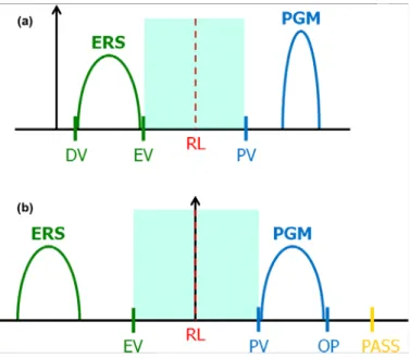
II.4 I-V curves of a FG devices with and without charge stored in the FG. 9 II.5 Schematic band diagram illustrating the “lucky electron model” 10 II.6 Schematic illustration of (a) NOR and (b) NAND architectures 12 II.7 (a) NOR and (b) NAND program windows. DV=Depletion Verify level;
EV=Erase Verify level; RL=Read Level; PV=Program Verify level;
OP=Over-Programming level; PASS=PASS voltage. 13 II.8 Schematic representation of the conduction band diagrams of various
tunnel barriers: (a) conventional SiO2 barrier; (b) ideal crested barrier; (c)
real crested barrier [38]. 17
II.9 Band diagrams illustrating the VARIOT concept for the case of (a)
two-layer (asymmetric) barrier and (b) three-two-layer (symmetric) barrier [40]. 18
II.10 Cross section of a NROM device. 20
III.1 Flowchart of the statistical MC simulator 23
III.2 Schematic representation of a symmetric SiO2/high-k/SiO2 dielectric stack
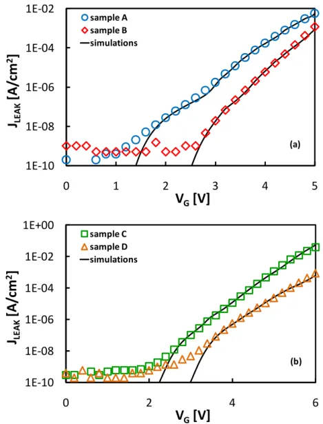
showing some key parameters used in simulations 24 III.3 Comparison between experimental and simulated leakage currents across
(a) SiO2/HfO2 and (b) SiO2/HfSiON large area capacitors 27
III.4 Comparison between experimental and simulated leakage currents across
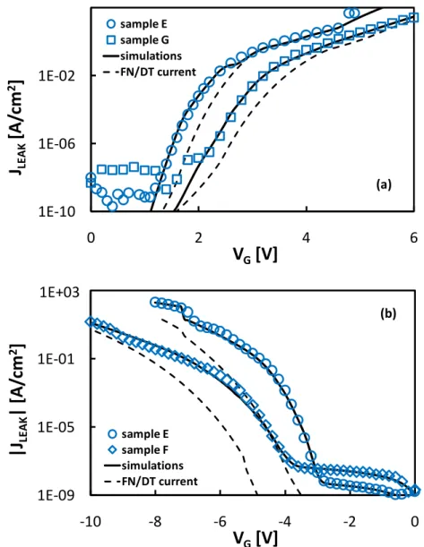
SiO2/Al2O3 stacks under (a) substrate and (b) gate injection conditions. 28
III.5 JLEAK.vs VG curve simulated considering interface defects (INT), oxide
defects (OX), and high-k defects (HK), in addition to the FN/DT current
contribution 29
III.6 Leakage current simulated and measured on sample B at different
temperatures. Symbols: experiments; lines: simulations. The inset shows
the Arrhenius plot at VG=4V. 29
III.7 Comparison between experimental and simulated leakage currents across
III.8 Comparison between ideal leakage currents simulated considering
SiO2/HfO2 (sample B in Table III.1) stack and pure SiO2 capacitors with
the same EOT=4.5nm. 31
III.9 Statistical distributions of JLEAK at VRET for SiO2/HfO2 and SiO2/HfSiON
stacks having EOT=4.5nm. Dashed lines depict Direct Tunneling (DT)
currents 32
IV.1 (a) Linear and (b) logarithmic ID-VGS characteristics measured at 300K
(filled symbols) and 360K (empty symbols) for a fresh cell (A), and for
devices programmed to different levels (B, C and D, as in [80]). 36 IV.2 Schematic cross section zoom of rectangular charge distributions defined
into the nitride layer of the device. Only narrowest and largest LCN cases
are shown. 37
IV.3 Total charge as a function of LCN for the considered rectangular charge
distributions, see Table IV.I. The amount of charge needed to obtain the same VTR is approximately constant with respect to LCN. 38
IV.4 Temperature Monitor curves corresponding to cells in condition A (initial)
and programmed to B, C and D levels. 39 IV.5 TM curves corresponding to the rectangular charge distributions in Fig. 2,
for VTR = VTR,FRESH + 2V. 40
IV.6 LCN as a function of ΔTMMAX for cells whose VTR shift is 0.5 V, 1 V, 1.5
V, and 2 V higher than the threshold voltage of the virgin cell (from the
left to the right). 41
IV.7 ID – VGS curves corresponding to the rectangular charge distributions in
Fig. 2, for VTR = VTR,FRESH + 2V. 42
IV.8 LCN as a function of ΔSSR. 43
IV.9 Schematic cross section of the triangular charge distributions calculated for
NROM cells programmed at B, C and D levels. 44 IV.10 Matching between measured (symbols) and simulated (lines) ID-VGS curves
at both 300K and 360K. For the simulated curves, the triangular charge distributions sketched in Fig. 9 were defined into the nitride layer of the
device. 45
IV.11 Schematic cross section of the triangular distributions calculated for
NROM cells programmed at D level with different VGS. As program VGS
increases, LCN is reduced. 46
IV.12 TM curves corresponding to cells initially programmed to level D and
erased to level C with positive (empty triangles) and negative (empty
IV.13 Schematic cross section zoom of hole distributions superimposed on the
electron distribution derived for program level D. The hole density was adjusted in order to obtain half erased and fully erased conditions. 47 IV.14 Current density along a vertical cut in the channel at 2nm from the drain
junction (i.e. under the nitride charge region). The gate of the device is biased at 1.5 V, corresponding to a device operating in subthreshold regime. Continuous and dashed lines refer to half erase and full erase
conditions, respectively. 48
V.1 Experimental ID-VGS (a) and ID,GIDL-VGS (b) characteristics for NROM
cells programmed (filled symbols) and negatively erased (empty symbols) to different levels. DVTR is relative to the threshold voltage of a fresh
device. 53
V.2 Flowchart of the methodology proposed to profile hole charge distribution. 54 V.3 Schematic cross section of the rectangular hole distributions superimposed
on the program distribution to analyze the impact of CCN and QTOT,H on
VT,GIDL. 56
V.4 CCN vs. ΔVT,GIDL plot extracted from simulated FE conditions. Empty and
filled symbols correspond to negatively and positively erased devices, respectively. Each symbol corresponds to a different width of the
considered hole distribution. 57
V.5 QTOT,H vs. ΔVT,GIDL plot extracted from simulated FE conditions. Empty
and filled symbols correspond to negatively and positively erased devices, respectively. Each symbol corresponds to a different width of the
considered hole distribution. 57
V.6 Evolution of total electrons and holes charge in the nitride. The labels “P”
and “E” refer to program and erase operation, respectively. Positive (negative) values on the x-axis correspond to the junction (channel) region
of the device. 58
V.7 Comparison between experimental (symbols) and simulated (lines) GIDL
on characteristics for the negative erase case. Simulations were carried out by inserting derived hole distributions into the nitride layer. Both (a) linear
and (b) logarithmic scale are shown. 59 V.8 Simulated JCHEI profile at the beginning of the second program operation
are compared with the JCHEI profile simulated for a fresh device. Positive
(negative) values on the x-axis correspond to the junction (channel) region
V.9 Erase state retention losses as a function of the applied erase scheme (a).
The retention losses simulated by assuming the hole charge redistributions sketched in (b)-(c) are also shown (stars). The shaded area in (b)-(c) represents the region of maximum sensitivity of VTR against hole charge
position. 61
V.10 Variations of VTR and VT,GIDL as a function of the retention time, for a
device half erased under a positive erase scheme. The inset shows
logarithmic ID,GIDL-VGS curves for two different retention times. 62
VI.1 (a) Cross section schematic of the TANOS memory devices used in this
work. (b) Schematic flow chart of the model describing VT shift during
program operation. 65
VI.2 Schematic representation of CB diagram and charge fluxes considered in
the model. Index “i” and “j” refer to space and time discretization, respectively. JIN is the current entering the nitride region, JTRAP and JEM are
the charge fluxed related respectively to capture and emission processes, JTUN and JOUT are the currents entering and leaving the nitride at the
SiO2/Si3N4 and Si3N4/Al2O3 interfaces, respectively. 66
VI.3 Measurements (symbols) and simulations (lines) of VT shifts in TANOS
memory (sample C) when varying the gate voltage VG. A uniform trap
density across the nitride of NT=7.5⋅1019 cm-3 is considered with σT=7⋅10-15
cm2. Dashed lines in the inset depict simulations performed not considering
TAT in the calculation of the program current density. 68 VI.4 Comparison between VT shifts measured (symbols) and simulated (solid
lines) for sample D. Simulations include both thermal and tunnel-based
emission contributions. 69
VI.5 Comparison between VT shifts measured (symbols) and simulated (solid
lines) for sample C. Simulations include both thermal and tunnel-based
emission contributions. 70
VI.6 Charge centroid CCN normalized with respect to the thickness of the nitride
layer as a function of the equivalent electric field across the tunnel oxide. The inset shows the evolution of the charge centroid with program time at different program voltages (sample C). EOT is the Equivalent Oxide Thickness of the stack, whereas VG is the voltage applied during program.
List of Tables
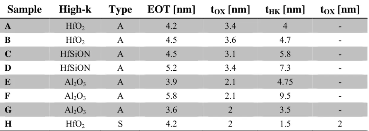
III.1 Main characteristics of the dielectric stacks used. The “Type” column refers
to the type of dielectric stack: Symmetric (S) or Asymmetric (A). 26 III.2 SiO2 and high-k parameters used in leakage simulations. 26
III.3 Trap parameters used in simulations. The indexes OX, INT and HK refer to
traps in oxide, at the interface(s) and in the high-k, respectively. 26
IV.1 Experimental Values of SSR and TMMAX. 40
IV.2 Relative uncertainties calculated for LCN. 45
IV.3 SSR and TMMAX values extracted from simulations for HE and FE cells. 47
V.1 Maximum values of simulated JHHI and JE profiles for devices at the beginning (INITIAL) and at the half (HE) of the erase operation for both positive and
negative erase. 55
CHAPTER
I
Introduction
INCE their introduction in 1984, Flash memory devices have followed Moore’s law keeping their structure basically unchanged. This era of happy scaling is now ending as Floating Gate (FG) devices – the mainstream Flash technology – cannot be further shrunk due to severe physical and technological limitations. As happened with the introduction of high-κ/metal gate structures for logic in late 2007, the time for innovation has come also for Flash memory devices.
Extensive research efforts are today devoted to the investigation of alternative non-volatile memory (NVM) devices able to overcome FG limits, thus enabling the scaling of Flash technology under the 30-nm technology node. Among the wide number of solutions proposed in the last years, nitride-based charge-trapping (CT) and bang-gap engineered (BGE) devices are two of the most promising technologies. This work describes part of the research on these topics author has been involved in during the XXI ciclo, Dottorato in Scienze dell’Ingegneria doctorate course.
Chapter II will give a thorough overview of FG Flash technology. After some
considerations on current status and future trends of the NVM market, the main limits of the floating gate transistor will be discussed for both NOR and NAND architectures. Then, a quick overview of the most interesting innovative devices proposed for the post-Flash scenario will be given. Particular care will be devoted to charge-trapping and bang-gap engineered devices, as they are the topic of this thesis work. Their operating principles and expected improvements with respect to FG devices will be discussed and investigated.
In Chapter III, the statistical Monte Carlo (MC) simulator developed to reproduce leakage currents flowing through high-κ based layered structures will be introduced. We will show that simulations reproduce accurately experimental data measured on large area capacitors having both symmetric (SiO2/high-κ/SiO2) and asymmetric (SiO2/high-κ) gate
stacks, proving that the model catches correctly leakage current conduction mechanism
physics, thus being a valuable tool to investigate defect properties of high-κ composite dielectrics. Feasibility and optimization of band-gap engineered barriers for future NVM generations will be then investigated. Statistical simulations will be exploited to assess the real benefits of high-κ stacks as Flash memory tunnel dielectrics considering a 1Mb array of 65nm NAND Flash cells. We will show that the strong reliability improvements predicted by the adoption of BGE barriers disappear when trap-assisted contributions are included, warning on the possibility of replacing conventional tunnel oxides with the high-κ stacks
Author’s research work on charge-trapping devices will be presented in the next three chapters. Chapter IV will present two tools allowing to profile program charge distributions in NROM devices based on ID-VGS sensitivity on local charge storage. Compact formulas to
calculate length and density of the program charge distribution will be derived, and their accuracy will be tested for cells programmed at different levels and under different bias conditions. Tools accuracy and sensitivity will be investigated, and their limits when applied to erased NROM cells will be discussed.
As the tools presented in Chapter IV are sensitive only to the net charge above the channel, a new technique to profile hole distributions in erased NROM devices, which combines compact models, device simulations, and Gate-Induced Drain Leakage (GIDL), will be presented in Chapter V. Electron discharge effects are also taken into account, and the accuracy of the final charge scenario obtained will be verified by comparing drain and GIDL experimental currents to simulations. The technique will be used to monitor charge evolution after program and erase operations, allowing explaining some general mechanisms related to NROM reliability. First, it will be demonstrated that in cycled devices the amount of electrons in the nitride portion above the channel increases, because holes injected above the junction during erase shift the lateral field peak into the channel. Second, we will prove that VTR drifts
occurring in NROM cells left unbiased in the erased state are due to the lateral migration of trapped holes. The model presented allows explaining also the polarity dependence of the VTR
drift on the erase scheme adopted.
Chapter VI will describe a new physics-based model to simulate program transients of
nitride-based future generation NAND devices (TANOS). Experimental results measured on TANOS devices with different oxide and nitride thicknesses will be reproduced with a great accuracy using an unique set of parameters, proving that the model catches correctly TANOS programming physics. In particular we will show that trapping process is independent from the energy of injected electrons, according to conventional Shockley-Read-Hall (SRH) theory, while electron de-trapping is dominated by tunneling. Finally, the evolution of the nitride charge during program will be investigated. We will show that the charge centroid is almost constant during the program transient and depends on the thickness of the nitride layer. These information are crucial for the optimization of TANOS memory cells.
CHAPTER
II
Flash Memories: Past, Present and Future
“I do not see why somebody should need more than 64K of memory”
Bill Gates
The aim of this chapter is to provide a thorough overview of state-of-the-art Flash memory cells. Operating principles, charge injection mechanisms and scaling limits of Floating Gate devices are quickly reviewed. Then, an overview of the most interesting innovative devices proposed in the literature is presented, devoting particular attention to charge-trapping and bang-gap engineered devices, as they are the topic of this thesis work.
INCE the introduction of the first device in 1984 [1] the Flash memory market has been continuously growing, driven by the increasing number of applications demanding for a flexible, low-cost and reliable solid-state memory. Historically, the three major markets for Flash memories have been related to Personal Computers (PC), wireless and telecom applications, and automotive electronics. More recently, Flash memory market has been driven by the large mass success of new portable electronic equipments like mp3 audio players, USB storage devices, smart cellular phones and digital cameras.
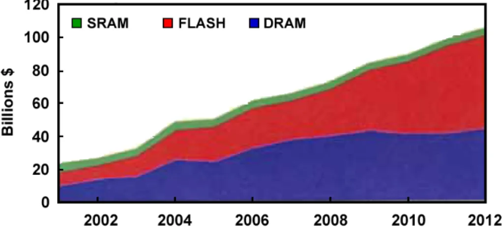
The evolution of the whole semiconductor and Non-Volatile Memory (NVM) markets are shown in Fig. II.1(a) and (b), respectively [2]. As can be seen, computers have been the main market driver for years. This means that devices such as DRAMs and Microprocessors have driven the largest sales and volumes of IC companies, see Fig.II.1(a)-(b). Nevertheless, NVM market share is constantly increasing, mainly because of the high demand for high-capacity non-volatile memory devices for portable applications, see Fig. II.1(b).
In 2006, the Complementary Metal Oxide Semiconductor (CMOS) memory market accounted for 23% of the total IC market with $58B sales, see Fig.II.1(a). Of these, $12B come from NAND Flash memories, while $9B were from NOR type Flash1. As can be noticed in Fig. II.1(b), the most growing semiconductor memory is Flash, especially NAND architecture, which sales increased exponentially since their introduction. On the contrary, NOR sales have been almost constant since 2001.
Presently, the Flash NVM market is in the range of $20 billions, but it is forecasted to grow with a higher average annual rate than DRAM and SRAM, reaching the $50 billions in 2011, see Fig. II.2.
1 NOR and NAND architectures will be discussed in Paragraph II.3.2.
II.1 Applications
Flash memories have two major applications: one is the code application, i.e. the possibility of nonvolatile memory integration in logic systems to allow software updates, store identification codes, or reconfigure the system on the field.
In this sense, Flash devices are widely used in several fields. In the computer environment they allow to store and update the operating system in PC BIOS and Hard-Disk Drives (HDDs), in almost all peripherals like printers and DVD-readers, and in most add-on boards like video and sound cards. On computer network equipments, they allow to quickly upgrade the software in modems, interface cards and network routers. In the automotive electronic field they are used in vital functions such as Engine Control Units (ECUs) and Global Positioning Systems (GPS). Finally, cellular phones are a key Flash marked driver in years, with their demand for an always increasing amount of reliable and low-power memory devices.
The second application, called data application, is to create storing elements like memory boards or solid-state hard disks, made by Flash memory arrays, which are configured to create large size memories.
In this field, besides the well established USB storage devices that have now reached the incredible size of 64GB, the growth and advancements in Flash technology have enabled a significant opportunity for Solid-State Drives (SSDs) to make tangible inroads into markets currently dominated by HDDs. For example, Toshiba recently announced (Dec. 2008) the first 512GB SSD, which uses 43nm Flash technology to fit into a standard 2.5-inch drive casing and is expected to undergo mass production in mid 2009.
II.2 Fundamentals of NVMs
To have a memory cell that can commute from one state to the other, and which can store the information independently of external conditions, the storing element needs to be a device whose conductivity can be changed in a non-destructive way. One solution is to have a transistor with the threshold voltage that can change repetitively from a high to a low state, corresponding to the two states of the memory cell, i.e. the binary values “1” and “0” of the stored bit.
The threshold voltage VT of a MOS transistor can be written as [3]:
OX T C Q K V = − (II.1)
where K is a constant that depends from gate oxide thickness, doping, gate and substrate materials, Q is the charge weighted with respect to its position in the gate oxide, and COX is
the gate oxide capacitance. It is evident from above equation that the threshold voltage of the MOS transistor can be altered by changing the amount of charge present in the insulator. Two are the main solutions adopted.
The most common way is to store the charge in a conductive layer between the gate and the channel that is completely surrounded by insulator. Since this layer acts as a completely electrically isolated gate, this type of device is commonly referred to as a Floating Gate (FG) device [4]-[6]. These devices still represent the mainstream technology and will be discussed more in detail in the next paragraph.
An alternative solution is to store the charge in discrete trapping centers of an appropriate insulating layer. The most commonly used material is nitride [7]-[10], with new materials being currently investigated [11]-[13]. These devices are called charge-trapping (CT) devices and have been introduced almost simultaneously to the FG transistor [7]. Today they are considered one of the most promising alternative to FG devices for future technology nodes [9], [14]. They will be treated more in detail in Paragraph II.4.2.
II.3 The Floating Gate Device
Most of the modern non-volatile memory devices are based on the Floating Gate (FG) transistor, whose structure is depicted in Fig. II.3. The upper gate is the control gate (CG) and the lower one, a conductive layer completely surrounded by dielectric, is the FG.
The FG is electrically isolated from source, drain and bulk regions through a high-quality thermal oxide called tunnel oxide, whereas CG and FG are separated by the Inter-Poly Dielectric (IPD), often called control oxide. The basic concepts and functionality of a FG device can be easily understood by determining the relationship between the FG potential, that physically controls the channel conductivity, and the control gate potential, controlled by external circuitry [15]. This can be done using the simple electrical model (known also as capacitive coupling coefficient model) shown in Fig. II.3(b). CCG, CS, CD, and CB are the
capacitances between FG and CG, Source (S), Drain (D) and Body (B), respectively. If no charge is stored in the FG, i.e. Q = 0:
(
FG CG)
S(
FG S)
D(
FG D)
B(
FG B)
FG V V C V V C V V C V V
C
Q= 0= − + − + − + − (II.2)
where VFG is the potential on the floating gate, VCG is the potential on the control gate, VS,VD,
VB are potentials on S, D and B, respectively. If we name CT = CFG+CD+CS+CB the total
capacitance of the FG, and we define αJ = CJ/CT as the coupling coefficient relative to the
electrode J, where J can be one among CG, D, S, and B, the FG potential is given by
B B S S D D CG CG FG V V V V V =α +α +α +α (II.3)
It is interesting to note that the Floating Gate voltage does not depend only on the control gate voltage, but also on source, drain and bulk potentials. Moreover, if source and body are both grounded Eq. (II.3) can be rearranged and reduces to
(
CG DS)
CG FG V f V V =α + ⋅ , where CG D CG D C C f = = α α (II.4)Figure II.3: a) Schematic cross-section of a Floating Gate transistor; b) electrical model
Device equations for the FG MOS transistor can be obtained from the conventional MOS transistor equations by replacing MOS gate voltage, VGS, with VFG, and transforming the
device parameters, such as threshold voltage, VT, and conductivity factor, β, to values
measured with respect to the control gate: VTCG = αCG⋅VTFG and βCG = βFG/αCG [15].
Thus, the current-voltage (I-V) equations of FG MOS transistor in both Triode Region (TR) (II.5) and in the Saturation Region (SR) (II.6), can be easily derived from that of a conventional MOS transistor [16].
TR:
(
)
⎥ ⎦ ⎤ ⎢ ⎣ ⎡ ⎟⎟ ⎠ ⎞ ⎜⎜ ⎝ ⎛ − − − = 2 2 1 DS CG DS CG T CG CG DS V V V f V I α β CG T DS CG G DS V fV V V <α + − (II.5) SR:(
)
2 2 CG T DS CG CG CG DS V fV V I = β α + − CG T DS CG CG DS V fV V V ≥α + − (II.6)These equations underline some major differences between I-V characteristics of FG and conventional MOS transistor [16] that are mainly due to the capacitive coupling between drain and floating gate. Two of them are worth to be mentioned.
First, the FG MOS transistor can conduct current even when |VCG-VS| < |VT|, because the
channel can be turned on by the drain voltage through the f⋅VDS term in (II.4).
Second, in the saturation region IDS continues to rise as the drain voltage increases: no
saturation will occur. Thus, IDS results to be dependent on VDS, on the contrary to what
happens in conventional MOS transistors.
If some charge is stored in the FG, i.e. Q ≠ , all the hypotheses made above hold true, 0 although the following modifications in the VFG and VT calculation need to be included
T DS D CG CG FG C Q V V V =α +α + (II.7) CG CG 0 T CG T C Q V V = − (II.8)
VT0 is the threshold voltage when Q=0. From (II.8), we can see that the role of injected
charge is to shift VT, i.e. the I-V curves of the cell, by the amount –Q/CCG. If the reading
biases are fixed, the presence of charge greatly impacts the current level of the cell state. At this regard, Fig. II.4 shows two I-V curves: curve A represents the “1” state, whereas curve B the “0” state of the same cell.
II.3.1 Charge Injection Mechanisms
Among the several mechanisms that can be used to transfer charge from and into the FG, two are the ones currently used in industry-standard FG devices: Channel Hot Electron (CHE) injection [17], which is used for the program operation, and Fowler-Nordheim (FN) tunneling [18], used for both program and erase operations.
Channel Hot Electron Injection. The physical mechanism of CHE injection is relatively
simple to understand qualitatively. An electron traveling from the source to the drain gains energy from the lateral electric field and looses energy to the lattice vibrations (acoustic and optical phonons). At low fields, this is a dynamic equilibrium condition, which holds until the field strength reaches approximately 100 KV/cm [19]. For fields exceeding this value, electrons are no longer in equilibrium with the lattice, and their energy begins to increase. Electrons are “heated” by the high lateral electric field and a small fraction of them gains enough energy to surmount the oxide barrier. For an electron to overcome this potential barrier, it must have kinetic energy higher than the potential barrier and velocity directed towards the FG [20].
A simple description of the CHE injection mechanisms can be given following the lucky
electron model [17]. This model is based on the probability for an electron to be lucky enough
to travel ballistically for a distance several times the mean free path without scattering, eventually acquiring enough energy to cross the potential barrier if a collision pushes it towards the Si/SiO2 interface. Consequently, the probability of injection is the lumped
probability of the following statistically independent events, see Fig. II.5: 1) the carrier is “lucky” enough to acquire the energy to overcome the oxide barrier and to retain this energy after the collision that redirects it towards the interface (Pφb); 2) carrier follow a collision-free
path from the redirection point to the interface (PED); 3) the carrier can surmount the repulsive
Erased (1) Programmed (0) VT0 VREAD VT ID VGS ΔVT= -Q/CCG A B
oxide field at the injection point without suffering an energy-robbing collision in the oxide (POC). CHE injection is a fast program mechanism, but has a poor efficiency and leads to a
large power consumption.
Fowler-Nordheim Tunneling. The solution of the Schrödinger equation shows that a
tunneling through a potential barrier is possible even for classically forbidden barriers [22]. The probability of electron-tunneling depends on the distribution of occupied states in the injecting material and on the shape, height and width of the potential barrier. Using a free-electron gas to model the free-electron population in the injecting material and the Wentzel-Kramers-Brillouin (WKB) approximation to calculate the tunneling probability [23], the well known expression for FN current density can be obtained [24]
⎟⎟ ⎠ ⎞ ⎜⎜ ⎝ ⎛ − ⋅ = OX FN OX FN FN F B F A J 2 exp (II.9)
where FOX is the oxide field, T is the temperature and AFN and BFN are coefficients that can be
calculated from MOS physical constants [24].
0 2 3 16 Φ = OX Si FN m m q A h π qh m BFN OX 3 2 4 3 0 Φ = (II.10)
q is the electron charge, and h is the reduced Plank’s constant; Φ0 is the oxide barrier height;
mSi and mOX are the electron effective masses in the silicon and in the oxide layers,
respectively.
The optimum thickness (about 7-8 nm) for FG memory using tunneling phenomenon is chosen trading off between performances constraints (programming speed, power consumption, …) which would require thin oxides, and reliability concerns, which would require thick oxides. Moreover, tunneling currents are also important for device-reliability at low fields. In the case of bad-quality tunnel oxides, or when thin oxides are stressed many times at high voltages, Trap Assisted-Tunneling (TAT) through bulk traps either present or generated in the oxide can strongly enhance the tunnel current. Therefore, oxide defects must be avoided to control program/erase characteristics and to have good reliability. This aspect is particularly important also for BGE devices and will be further discussed in Chapter III.
Although being slow with respect to CHE injection, FN tunneling is highly efficient: the only current flow produced into the cell is the tunneling current across the oxide, and all the transferred charge contributes to the modification of the FG charge state.
II.3.2 Flash Architectures
Two types of array organization are currently used for Flash devices: the NOR and the NAND architectures (see Fig. II.6). Both were invented by Fusjio Masuoka2 (Toshiba) and respond to the different needs of code and data applications.
NOR architecture [1] is the most commonly used for code storage, since it guarantees the fast random access times required by this kind of applications. The NOR array is sketched in Fig. II.6 (a): all gates of the cells belonging to the same row are connected to the same wordline, whereas all drains of the cells in a column are connected to the same bitline; the sources of all the cells in the same sector are connected to a common source line. Programming is performed by means of CHE injection, whereas erasing is performed through FN tunneling. The thickness of the tunnel oxide is currently in the range of 7-8nm [26] and cannot be scaled below this value due to retention reliability issues (see paragraph II.3.3).
Beside common NOR, parallel architecture, Flash memories can also be organized in NAND arrays [27], by connecting 32 or even 64 cells in series between a bitline and the sourceline, as depicted in Fig. II.6(b). The main advantage of this solution is the achievement
2 Masuoka worked on his ideas without permission from Toshiba. By 1980 he had already applied for the basic patents on NOR-type Flash memory, but it was not able to produce the first device until four years later, after a promotion (before, he was not senior enough to be allowed to go to the factory without permission and order them to make him some devices). Masuoka presented his Flash memory at the annual International Electron Device Meeting, in 1984. Intel immediately put more than 300 engineers to work full time on developing Flash memory, whereas Toshiba assigned only five engineers to help Masuoka on a part-time basis. It was not long before Intel completely dominated the market.
In 1987, again without permission, Masuoka made the first batches of his new NAND-type Flash memory. This time he was senior enough to be able to devote resources to the project to ensure that Toshiba gained an insurmountable lead in both patents and production technology. However, shortly after the first of the new memories went on the market in 1990, Toshiba began pressuring him to accept a "promotion" that, at the ripe old age of 47, would have put him in a job with no subordinates. In 1994 he quit Toshiba to become a professor at Tohoku University. Adapted from [25].
of an higher integration density because of a decreased number of contacts, from one contact to the bitline for every cell as in NOR array, to one contact for 32/64 cells. On the other hand, the read operation is much slower with respect to NOR, as the whole string must be accessed. For these reasons, NAND Flash memories are limited to mass storage applications only3. Both program and erase operation are performed through FN tunneling. Although the scaling of the tunnel oxide for NAND Flash faces the same challenges as that for NOR Flash, the use of Error Code Correction (ECC) in NAND, together with the less stringent reliability requirements due to the target applications, allows thinner oxides to be used (6-7nm [26]).
A fundamental difference between NOR and NAND architectures is the threshold voltage (VT) range adopted for programmed and erased distributions, see Fig. II.7. In NOR
architectures the VT working range is higher than 1.5V and lower than 8V. Reading is
performed by biasing word and bitline of the selected cell to positive voltages, with the other
3 This was absolutely true in the past. Recently, new products that aim to combine the high density of NAND with the fast read of NOR have been proposed, e.g. Samsung’s OneNANDTM.
wordlines and bitlines grounded. Thus, the unselected cells sharing the bitline of the cell being read must have a VT > 0 to have a correct sensing of the cell’s state. In the NAND
architecture, the VT operating range is from -5V to +3V. In this case read is performed by
grounding the wordline of the selected cell and positively biasing the bitline and the wordline of the unselected cells belonging to the same string. The unselected cells act as pass transistors and the current flowing in the string is determined only by the state of the selected cell. Therefore, the unselected cells must have a threshold voltage lower than the pass voltage to read properly the state of the selected device.
II.3.3 Scaling Limits of FG Devices
To achieve higher densities and reduce costs, a reduction of device dimensions is required. Unfortunately, the scaling of conventional FG devices below the 45nm technology node appears critical, due to severe technological limits and reliability issues.
Tunnel Oxide Scaling. Program and erase operations of Flash memories require high
voltages, as they are based on physical mechanisms whose major parameters do not scale (3.1eV energy barrier for CHE injection and at least 10MV/cm for FN data alteration in 0.1s).
The simpler way to decrease writing voltages would be to reduce the thickness of the tunnel oxide. However, in order to guarantee at least 10 years of data retention, the tunnel oxide limit is fixed to 6nm by the direct tunneling mechanism, a value that needs to be
Figure II.7: (a) NOR and (b) NAND program windows. DV=Depletion Verify level; EV=Erase Verify level; RL=Read Level; PV=Program Verify level; OP=Over-Programming
increased to 7-8nm to account for the anomalous conduction through the tunnel oxide due to trap-assisted-tunneling caused by oxide aging [28]. This current is commonly referred to as Stress-Induced Leakage Current (SILC) and leads to a dramatic increase of the charge loss from the FG during retention. This phenomenon has been deeply investigated in the past [28]-[30] and depends mainly on stress magnitude and oxide thickness. It is generally assessed that the tunnel oxide cannot be scaled below 7-8nm to control SILC effects. A reduction of this limit requires the replacement of conventional SiO2 tunnel dielectric with BGE barriers, as
will be discussed in the next paragraph.
Gate Coupling Ratio (GCR). One of the major stumbling blocks for future FG devices is the
expected reduction of the coupling coefficient between CG and FG (αG in Eq. II.4). This
parameter determines the fraction of the voltage applied at the CG that is transferred to the FG: it must be higher than 0.6 in order to obtain reasonable writing voltages.
In current technologies, a high GCR is normally achieved by wrapping the control gate around the sidewalls of the floating gate4. However, below 40nm the spacing between FG may become too narrow for the IPD and CG to wrap around the FG, leading to a strong decrease of the GCR. To overcome this problem, innovative solutions are required, e.g. the replacement of ONO inter-poly dielectric with high-k materials [26].
Capacitance Coupling Between adjacent Cells (NAND). The continuous shrinking of
NAND memories lead to an enhanced capacitance coupling between adjacent cells, which significantly increases the lateral fringing field disturbing NAND operations [31]. 3D TCAD simulations show that the threshold voltage shift (ΔVT) induced by adjacent cells on the same
bitline (BL) and wordline (WL) increases exponentially with technology scaling, tripling moving from the 57nm to the 32nm technology node [32]. To reduce the FG interference it is necessary to thin the FG and to adopt low-k dielectric materials. An alternative is represented by CT devices that does not suffer from this problem.
4 Without this expedient, the required value of 0.6 could not be reached. The GCR is defined as the ratio between the CG to FG capacitance, CCG, and the total capacitance of the FG cell, CTOT (see paragraph II.3). Neglecting the contribution of CS and CD, it can be expressed as
TUN IPD G t t + = 1 1 α
where tIPD and tTUN are the thicknesses of IPD and tunnel layers, respectively. As typical values of tIPD and tTUN
are in the range of 7-8nm and 13-15nm, respectively [26], this leads to αG ranging from 0.32 to 0.41 for current technologies (a little bit pessimistic as CS and CD have been neglected).
II.4 Innovative NVM Devices
Extensive research efforts are today devoted to the investigation of alternative non-volatile memory devices able to overcome the FG limits discussed in the previous paragraph, thus enabling the scaling of Flash technology under the 45-nm technology node. The solutions that have been proposed in the last years can be classified into evolutionary and revolutionary concepts. The first class of devices adopts new materials and/or new storage mechanisms to push the traditional FG structure beyond its limits. BGE and CT devices belong to this category. On the contrary, revolutionary devices are based on completely new concepts in which the FG transistor is replaced by new storage elements obeying to a completely different physic to store the information. Some examples are Ferroelectric RAMs (FeRAMs), Magnetoresistive RAMs (MRAMs) and Phase Change Memories (PCMs).
A brief description of some of the most promising revolutionary devices will be given in the following. BGE and CT devices will be discussed more in detail in the next pharagraphs.
Ferroelectric RAMs. The operation of these devices is based on the ferroelectric effect [33],
i.e. the ability of a material to retain an electrical polarization in the absence of an applied electric field. This stable polarization results from the alignment of internal dipoles within the Perovskite crystal units in the ferroelectric material.
There are different approaches to implement these ferroelectric materials into a memory cell. A common one is to use a ferroelectric capacitor addressed by a transistor [34]. In order to sense the polarization state of the ferroelectric film in a capacitor, a switching of the polarization is required. Depending on the polarization state of the ferroelectric film, a small or a large amount of charge will flow in the circuit. However, a write back cycle is necessary in this cell concept in order to restore the initial read information. There are also concepts to realize non-destructive read-out cells, like the Ferroelectric Field Effect Transistor (FeFET) cell [35]. This cell type is a MOS transistor, where the gate oxide is replaced by a ferroelectric film thus giving the possibility of nonvolatile data storage in an extremely compact cell. The read-out is performed by sensing the source drain current, which is dependent on the threshold voltage given by the polarization state of the ferroelectric gate layer.
The main advantages of FeRAM devices are the fast read/write operation (around 100ns), high endurance (up to 1012 cycles) and low voltage write. However ferroelectric materials show some specific issues, like the decrease in switching polarity with cycling and the imprint phenomenon: the capacitor tends to prefer the state in which it has been for extended periods of time. The integration of ferroelectric materials in the CMOS process is also difficult.
magnetization directions and the read-out is done by a resistance measurement. Among the different MRAM concepts, the cell based on Tunneling Magneto-Resistance (TMR) is the most promising [36]. These devices use a Magnetic Tunnel Junction (MTJ) obtained with two stacked ferromagnetic layers. One of them has a fixed magnetization direction and is used as a reference layer, while the second can be switched between two states, thus representing the storage layer. The two ferromagnetic layers are separated by a very thin dielectric layer. The current flow through the structure is limited by this thin dielectric barrier and depends on the magnetic state of the two ferromagnetic films.
The MRAM cells are written by current pulses through the bit-line and the word-line in order to generate a magnetic field, which is larger enough to switch one of the ferromagnetic layers, but not large enough to switch the second magnetic reference layer. The magnetic domain switching and, thus, the writing time of the cells is in the range of a few ns and there is no endurance limit expected (in contrast with ferroelectric materials), since the electronic spin flipping mechanism does not degrade with continuous cycling.
Also MRAMs show some specific issues. The integration of the magnetic stack is a very critical point, due to the exact thickness definition of the insulating tunnel layer, which is required to avoid shorting between the tunneling electrodes. Another problem is the one associated with scaling. As the critical switching field (and thus the current density of the word line) becomes even larger upon shrinking the width of the cell size, a method for scaling the world line current has to be engineered in order to avoid electromigration and cross talk of neighboring cells.
Phase Change Memories. Phase Change Memory is another interesting competitor in the
class of nonvolatile memory contenders. This concept is based on the reversible phase change between the amorphous and the crystalline phase of a chalcogenide glass [37]. These two physical states of matter differ in their resistivity, as the conduction is generally much better in a crystalline chalcogenide than in an amorphous one due to the reduced scattering of charge carriers in films with atomic long range order. The transition from the crystalline to the amorphous state is performed by applying a very short electrical pulse to a resistive heater in contact with the phase change material thereby melting it (typical melting temperature is about 600°C) and thereafter rapidly cooling it to freeze the amorphous phase. In order to write the crystalline state into the cell a lower but a little bit longer pulse is applied, thus heating the material over the critical crystallization temperature (about 300°C in materials typically used) and leaving it in the low resistivity polycrystalline phase. The difference in resistivity of the two phases is about 2-3 orders of magnitude, which is considerably higher than in MRAM. The writing mechanism also allows the realization of Multi-Level Cell (MLC) data storage by programming the cell to intermediate resistance levels, thus yielding a lower fraction of the crystalline phase. Reading is accomplished by measuring resistance changes in the cell.
II.4.1 Band-Gap Engineered Devices
As discussed in paragraph II.3.3 the SiO2 tunnel dielectric cannot be scaled below 6-7nm in
order to guarantee data retention. This is clearly in contrast with the need to reduce program and erase voltages, which demands for a thinner tunnel oxide.
In order to scale the writing voltages while satisfying retention requirements, the thickness of the tunnel barrier should be reduced only during program and erase operations. In other words, the tunnel barrier should be thick in retention conditions and thin during program and erase operations, i.e. it should show an increased sensitivity on the applied voltage. This principle is at the basis of band-gap engineered barriers.
In BGE barriers, the conventional SiO2 tunnel oxide is replaced with a dielectric stack incorporating high-k materials, i.e. materials having a relative dielectric constant higher than the one of SiO2 (3.9). There are two possibilities: crested barriers [38], [39], that relies on the
concept of barrier height modulation (φ-engineering), and VARIable Oxide Thickness (VARIOT) barriers [40], which are instead based on the modulation of the electric field (κ-engineering).
The basic operating principle of crested barriers is sketched in Fig. II.8. For the case of a conventional rectangular energy barrier as the one depicted in Fig. II.8(a), the tunneling current varies slowly by increasing the applied voltage. This slow dependence of the barrier transparency on the electric field is due to the fact that the part of the barrier close to the electron source is only weakly affected by the applied voltage, see dashed lines in Fig. II.8(a).
Figure II.8: Schematic representation of the conduction band diagrams of various tunnel barriers: (a) conventional SiO2 barrier; (b) ideal crested barrier; (c) real crested barrier [38].
To increase the sensitivity of the energy barrier on the applied voltage, a “crested” barrier like the one depicted in Fig. II.8(b), with the potential barrier height peaking in the middle and gradually decreasing toward the electrodes, should be used [39]. The current through such a barrier changes much faster with the applied voltage. The reason is that the highest part of the barrier is pulled down by the electric field very quickly, see dashed lines in Fig. II.8(b).
The implementation of crested barriers is straightforward in composite semiconductors [38], but not in the case of a conventional CMOS process, as the ideal shape in Fig. II.8(b) cannot be achieved. A more practical solution is the one represented in Fig. II.8(c), where the ideal barrier shown in Fig. II.8(b) is approximated by a staircase energy barrier obtained with a dielectric stack. This kind of barrier can be obtained using high-k dielectrics, which typically have conduction band (CB) offsets with respect to silicon lower than the 3.1eV of SiO2 [41]. For example, the one depicted in Fig. II.8(c) is a tri-layered structure having a SiO2
layer sandwiched between two high-k layers. It is usually called symmetric crested barrier (high-k/SiO2/high-k) in contrast to the asymmetric one (high-k/SiO2), in which only one
high-k layer is used [39].
One of the main drawbacks of crested barriers is the requirement to have a high-k layer in direct contact with the silicon substrate. This leads to two major technological issues: i) an abrupt Si/high-k interface cannot be obtained, as a thin SiOX layer is usually formed ii) the
Si/high-k interface is usually of poor quality. These issues are not present in VARIOT engineered barriers, which can be considered an evolution of the crested barrier concept.
The operating principle of VARIOT BGE barriers is schematically represented in Fig. II.9. It relies on the fact that when a voltage is applied to the stack, the electric field
Figure II.9: Band diagrams illustrating the VARIOT concept for the case of (a) two-layer (asymmetric) barrier and (b) three-layer (symmetric) barrier [40].
redistributes in its layers being always higher in the one with the lower-k value (as a consequence of Gauss’ law). In addition, the high-k dielectric has typically a lower barrier height with respect to the SiO2 low-k dielectric: this means that for voltages higher than a
critical value electron tunneling (direct or FN) takes place only through the thin low-k layer,
see Fig. II.9. These effects determine a strong variation of the stack barrier with the applied bias and the stack can be regarded as a VARIable Oxide Thickness dielectric [40].
The VARIOT concept is very attractive for NVM applications since it theoretically allows to achieve a higher programming speed (or a lower voltage programming at the same speed), while guaranteeing the same retention performance of a conventional tunnel oxide [42]. Alternatively, BGE barriers can be optimized to improve Flash memory retention with respect to conventional SiO2, guaranteeing the same Program/Erase (P/E) performances.
Unfortunately, high-k materials feature very high bulk defect and interface state densities, and their theoretical advantages in retention improvement have to be weighed against their degraded parasitic trap-assisted leakage currents that lead to the undesired reduction of the threshold voltage. This aspect is very important in the assessment of real chances of high-k stacks to replace conventional SiO2 tunnel layers, as will be shown in Chapter III.
II.4.2 Charge Trapping Devices
The possibility to use trap-rich dielectric layers as the storage medium in charge-trapping non-volatile memory devices was recognized early [7]. Today these devices are considered one of the most promising alternatives to the FG technology, especially for NAND applications.
CT devices have two main advantages with respect to the conventional FG transistor. First, they have an inherent immunity to retention loss mechanisms related to point defects in the tunnel oxide (e.g. SILC). When a trap or percolation path is formed in the tunnel oxide, only the charge trapped in the portion of the nitride that is directly above it will discharge toward the substrate. As a consequence, the thickness of the tunnel oxide can be reduced well below the 6-7nm limit of conventional FG devices.
The second advantage is related to the interferences between adjacent cells. As discussed in Paragraph II.3.3, the continuous scaling of NAND memories lead to an enhanced capacitance coupling between adjacent cells: the threshold voltage of a cell depends also on the state of the adjacent cells. CT devices does not suffer from this issue: as the charge is localized, cross talk with neighboring cells is strongly reduced.
Among the different charge trapping devices that have been proposed in the literature [7]-[14] two are particularly promising: the NROM [10] and the TANOS [7]-[14] devices.
replaced with a nitride layer sandwiched between two silicon dioxide layers (forming the so-called ONO – Oxide-Nitride-Oxide – layered structure), as illustrated in Fig. II.10. The program operation is performed by CHE injection, whereas Hot Hole Injection (HHI) has been identified as the dominant erase mechanism [43]. The injected charge is stored in the nitride layer above the channel, in a very narrow region above the metallurgic junctions. The localization of the trapped charge, together with the reverse read methodology, allows storing two bits per cell [44]. Optimized technology, accurate and fast program algorithm, no single bit failures and window sensing with moving reference as an error detection and correction scheme, allow 4-bit product [45].
As already mentioned, reliability concerns that are crucial for the floating gate technology are of little importance for NROM memory devices. Electrons (or holes) are trapped individually and the loss of one charge through a defect does not affect other trapped charges that are not directly over the point defect (in contrast to FG technology). The specific reliability issues of NROM technology are associated with the localized trapping and with the presence of both electron and hole distributions in the nitride layer. In particular, lateral charge redistribution in the nitride may occur over time due to thermally activated charge migration between traps [46-49], thus leading to a threshold voltage shift over time.
To improve cell reliability and guarantee a correct cell operation also in scaled NROM devices, a deep knowledge of the charge distribution after both program and erase operations is needed. Different techniques developed during the Ph.D. research activity to profile electron and hole distributions in NROM devices will be discussed in Chapter V and VI.
TANOS Device. The TANOS cell structure was proposed by Samsung in 2003 [14]. It is an
evolution of the previously reported SANOS device [50], which in turn is an evolution of the SONOS device [8], [51].
Although allowing faster program and erase operations with respect to SONOS due to the introduction of the Al2O3 high-k dielectric as blocking oxide, original SANOS devices were
characterized by a reduced program window due to the fast saturation of the threshold voltage
during erase [50]. This saturation is attributed to electrons that are injected from the gate, thus compensating the effect of holes injected from the substrate [14].
To overcome the above mentioned issue, the TANOS structure was proposed, in which the poly-silicon gate used in the SANOS devices was replaced by a TaN metal gate [14]. This allowed to reduce the erase saturation level of approximately 2V. Such a significant improvement of the erase characteristics can be explained by the higher energy barrier that the electrons injected from the gate see at the TaN/Al2O3 interface.
Today, TANOS devices are considered one of the most promising candidate for scaled NAND Flash technologies. However, a deep understanding of the physical mechanisms involved in its operation is still lacking. In this sense, accurate models of program, erase and retention are highly needed, as they can providing important insights on trap characteristics, on the evolution of trapped charge during program and erase and on their dependencies on the TANOS stack composition. Such information are vital to for the optimization of TANOS memory cells. An accurate model of TANOS program transients will be presented in Chapter VI.
CHAPTER
III
Feasibility of BGE Barriers
“No exponential is forever… but we can delay forever”
Gordon Moore
In this chapter the feasibility of BGE barriers as Flash memory tunnel dielectrics in future Flash technologies is investigated. First of all, we describe the statistical Monte Carlo (MC) simulator developed to reproduce leakage currents flowing through symmetric and asymmetric high-k based layered structures. The simulator is validated against experimental data measured on large area capacitors having both symmetric (SiO2/high-k/SiO2) and asymmetric (SiO2 /high-k) gate stacks. Then, its statistical capabilities are exploited to assess the real benefits of the introduction of high-k stacks as Flash memory tunnel dielectrics in future Flash technologies. We simulate 1Mb array of 65nm NAND Flash cells in retention condition to extract the statistical distribution of the leakage current. We show that the strong reliability improvements predicted by BGE theory disappear when trap-assisted contributions are included. These results warn regardingthe possibility to replace conventional tunnel oxides with the high-k stacks.
IGH-K materials have been successfully introduced in the CMOS process to replace the conventional SiO2 as gate dielectric in 45nm logic transistors [52] and beyond.
They are also considered one of the most promising solution that has been proposed to overcome the limits of FG devices. Recently, they have been proposed both as storage layers in charge-trapping memories [11]-[13], and to replace conventional tunnel oxide to realize smarter band-gap engineered barriers [38]-[40].
In the framework of charge trapping memories, HfO2, HfSiON Al2O3 and more exotic
materials like Y2O3 [13] have been investigated as viable options to replace Si3N4 [10],
showing better charge-storage capabilities due to the very high trap density and the high permittivity.
On the other hand, band-gap engineered potential barriers have been introduced more than ten years ago [38], [39]. As discussed in Paragraph II.4.1, they theoretically allow improving Flash memory retention compared to conventional tunnel oxide, while guaranteeing the same Program/Erase performances.
Unfortunately, high-κ materials feature very high bulk defect and interface state densities, and their theoretical advantages in retention improvement have to be weighed against their degraded parasitic trap-assisted leakage currents that lead to the undesired reduction of the threshold voltage. This aspect is very important in the assessment of real chances of high-κ stacks to replace conventional SiO2 tunnel layers. In addition, when considering ultra-dense,
ultra-scaled Flash memory devices, the feasibility of BGE barriers has to be investigated also at the array level, accounting for the statistical effects related to the random position of defects in the gate stack. In this context, simulations are indispensable, as extensive reliability measurements on large Flash memory arrays are very time-consuming and costly [53].
III.1 Simulation Model
To simulate the leakage currents flowing through generic SiO2/high-κ dielectric stacks, we
extended the statistical Monte Carlo (MC) simulator used in [54]. Compared to the simpler SiO2 case, several issues related to the presence of a composite dielectric stack have to be
accounted for, such as the calculation of the electric field in different materials and of the tunneling probability between traps located in different dielectrics.
The block diagram of the MC simulator we developed is shown in Fig. III.1. It consists of three main parts devoted to electric fields calculation, random defect generation and leakage
Doping and geometry data Defect features (NT, ET, σT) and time (t*) Random defect generation Leakage current calculation
Calculate VTfrom IOXand time
VTdistribution
IOXdistribution
Electric fields calculation
current density (JLEAK) calculation, respectively. When the model is used to simulate leakage
currents flowing through the dielectric stacks of Flash memories, the device threshold voltage (VT) changes induced by JLEAK are calculated through an ad-hoc procedure, see Fig. III.1.
The electric fields across the dielectrics composing the stack are calculated with a model that takes into account poly depletion and charge quantization effects [55]. The presence of charge trapped in high-κ and oxide bulks and at the SiO2/high-κ interface is also included.
Defects are randomly generated within oxide and high-κ dielectric and at their interfaces, according to device geometry and defect statistics. Different densities (NT), cross sections
(σT), and energy distributions (ET) have been considered for different defects, as sketched in
Fig. III.2 for a symmetric barrier. For each of these features, we can select fixed as well as random values generated considering various statistical distributions. Noticeably, we can consider whichever physical defect distribution we want, not only the uniform one, which is usually considered for simplicity. This is very important to simulate the leakage current through thin gate stacks (EOT≈1-2nm) [56], as experimental evidences of non-uniform spatial distribution of defects have been reported already [57].
Once traps have been generated, JLEAK is calculated by summing both direct (JTUNN) and
defect-assisted (JPTAT) tunneling contributions. The conduction model we adopted is described
more in detail in the next section.
poly‐Si (or
metal gate)
Si
high‐κ
SiO
2φ
Bφ
offsetN
OX1, σ
OX1, E
T,OX1N
HK, σ
HK, E
T,HKSiO
2N
OX2, σ
OX2, E
T,OX2NINT1, σINT1,
ET,INT1
N
INT2, σ
INT2,
E
T,INT2Figure III.2: Schematic representation of a symmetric SiO2/high-k/SiO2 dielectric stack showing some key parameters used in simulations.

![Figure II.5: Schematic band diagram illustrating the “lucky electron model” [17].](https://thumb-eu.123doks.com/thumbv2/123dokorg/4724781.45819/26.892.303.632.125.389/figure-schematic-band-diagram-illustrating-lucky-electron-model.webp)
![Figure II.8: Schematic representation of the conduction band diagrams of various tunnel barriers: (a) conventional SiO 2 barrier; (b) ideal crested barrier; (c) real crested barrier [38].](https://thumb-eu.123doks.com/thumbv2/123dokorg/4724781.45819/33.892.256.683.126.454/figure-schematic-representation-conduction-diagrams-barriers-conventional-barrier.webp)
![Figure II.9: Band diagrams illustrating the VARIOT concept for the case of (a) two-layer (asymmetric) barrier and (b) three-layer (symmetric) barrier [40].](https://thumb-eu.123doks.com/thumbv2/123dokorg/4724781.45819/34.892.253.684.102.455/figure-diagrams-illustrating-variot-concept-asymmetric-barrier-symmetric.webp)