SCUOLA DOTTORALE
EDEMOM
European Doctorate in Electronic Materials,
Optoelectronics and Microsystems
XXIII CICLO DEL CORSO DI DOTTORATO
Development and Characterization
of Monocrystalline CVD Diamond
Linear X-Ray Dosimeters
Dottorando
Ing. Daniele Maria Trucchi
A.A.
2010/2011
Tutor Prof.
Gennaro
Conte
Contents
Introduction………..
Chapter 1. X-Ray Properties and Dosimetry……….…..7
1.1 Radiation dosimetry………....7
1.2 X-ray properties………10
1.2.1 X-ray source spectrum ………12
1.2.2 Characteristic X-ray lines………..……..12
1.2.3 Bremsstrahlung spectrum………..…..16
1.2.4 X-ray treatment – filtering………..…….16
1.3 X-ray sources………18 1.3.1 X-ray Tubes……….18 1.3.2 Radioactive sources………..23 1.3.3 Synchrotron radiation……….……..24 1.3.4 Plasma Sources……….…….26 1.4 X-ray detectors……….…….27 1.4.1 Gas Detectors………...27 1.4.1.1 Ionization chamber………..27 1.4..1.2 Proportional counter………..28 1.4.1.3 Geiger-Muller counter………....29 1.4.2 Solid-state Detectors……….30 1.4.2.1 Scintillators………...30
1.4.2.2 Semiconductor based detectors...30
1.4.2.3 Photodiodes………..…31
1.5 Photon Energy Loss in Matter………..32
Chapter 2. Physical Properties of CVD Diamond……….36
2.4 Charge carriers mobility and lifetime………...46
2.5 Surface conductivity. Hydrogenation………...47
Chapter 3. Technology and Development of CVD Diamond Dosimeters………...53
3.1 CVD Diamond samples………53
3.2 Metal-diamond contacts………...55
3.2.1 Specific contact resistivity………...56
3.2.2 Schottky junctions………..57
3.2.3 Ohmic junctions……….58
3.3 Development of the dosimeters……….……61
3.3.1 Substrate cleaning procedure………..62
3.3.2 Preparation of photolitographic masks……….62
3.3.3 Metallization………...63
3.3.4 Limited-size technological issues………68
3.4 Encapsulation………69
Chapter 4. X-Ray Experimental Setup………...74
4.1 Sources and filtering……….74
4.2 Absolute dose-rate measurement………..78
4.3. Device-under-test motion system and centring………79
4.4 DC irradiation………79
4.5 AC irradiation………81
4.5.1 X-ray shutter and mechanical chopper……….81
4.5.2 AC signal preamplifier……….82
4.5.3 Lock-in amplifier………84
Chapter 5. Evaluation of Dosimeters Performance………...86
5.1. Pre-irradiation characterization………86
5.1.1 Electric resistivity and leakage current……….87
5.1.2 Spectral photoconductivity measurements………...88
5.2 Priming process……….92
5.2.1 Priming process in optical-grade samples………93
5.2.2 Priming process in electronic-grade samples…………..95
5.3 Photo-detection model………..96
5.4.2 Signal stability and fluctuations………101
5.4.3 Dosimetric evaluation……….102
5.4.4 Transient DC analysis in optical-grade samples……..104
5.5 Specific Sensitivity………..106
5.6. Characterization by modulated irradiation (AC)………108
5.6.1 Frequency dependent signal………..109
5.6.2 Signal phase shift analysis……….110
Conclusions……….113
Introduction
Several medical applications rely on the interaction between high-energy radiation and human tissue. Radiotherapy, radiography, and mammography need a very precise measurement of the radiation dose imparted to the target volume. These techniques differ in the radiation wavelength, but all require reliable, precise, and sensitive detectors to accurately calibrate the radiation sources and/or directly monitor the dose delivered to a patient.
The aim of this thesis is to prepare radiation-sensitive dosimeters that could be finally employed especially for radiotherapy applications, a sector that is currently under strong technological development. Radiotherapy as well as all the medical applications concerning interaction between a high-energy beam and human body need strict requirements about the beam monitoring dosimeters:
a) resistance to radiation damage;
b) tissue equivalence to avoid corrections on the dose actually absorbed by human tissue; c) signal reproducibility and stability;
d) response proportional to the absorbed radiation dose-rate over a wide range of energies; e) response proportional to the accumulated dose;
f) response independent of the radiation quantum energy; g) response independent of temperature;
h) radiation sensitivity as high as possible; i) small size.
Moreover, recent radiotherapy techniques as the intensity modulated radiotherapy (IMRT) employ time-pulsed beams with small spatial size that need fast-response detectors. The additional requirement for a compliant detector for this technique is thus:
j) Response times <0.1 s.
The reference dosimeters for this kind of applications are the ionization chamber for gas-detectors and silicon photodiode for solid-state gas-detectors. Both have advantages and disadvantages.
dose, but lacks in sensitivity and in scalability: it cannot be miniaturized owing to intrinsic technological limitations. Moreover, ionization chamber is a slow-response detector that cannot be used in IMRT applications. Silicon photodiodes have a high radiation sensitivity and is compliant to miniaturization, but they lack mainly in radiation damage resistance and tissue-equivalency. In fact, the signal produced by silicon photodiodes has to be corrected with procedures that could induce errors in evaluating the actual dose absorbed by a patient.
To tackle the described requirements, a possible alternative material has to be found. Diamond is the most suitable material for intense x-ray dosimetry, since it shows properties of tissue equivalence, radiation hardness and chemical inertness. Such characteristics imply no energy corrections with respect to human tissue and long operative lifetimes. X-ray detectors based on geological diamond are commercially available, but their use is limited by high-cost selection and calibration of stones with appropriate physical properties. Synthetic diamond produced by chemical vapour deposition (CVD) has the potential to overcome such limitations, ensuring minor production costs and reproducible physical properties. Many research groups reported results on polycrystalline diamond films as a radiation sensitive material, but problems of signal stability and material homogeneity hampered the transition from a research to a production level. Recent technological advances in CVD diamond homoepitaxy allowed single-crystal films to become a standard material, with physical properties even superior than natural diamond.
The scientific and technological challenge of this thesis is focused on the development of single-crystal CVD diamond dosimeters by preparing device structures able to comply a number as high as possible of the described requirements. In order to perform this, two commercial families of single-crystal diamond films are employed to develop x-ray dosimeters: optical-grade and electronic-grade samples. They differ in the physical properties and in the so-called electronic quality. Obviously they differ very sensibly in cost. Our aim is to qualify their properties which more relevantly influence their performance by means of our characterization techniques. The comprehension of the mechanisms at the basis of their operative function is fundamental to improve their performance. An experimental setup based on x-ray photoconductivity has been completely renewed and designed to provide the most accurate and detailed analysis of their response.
The main objective is to demonstrate that the dosimeters resulting from an appropriate device design combined with low defected crystals can be even commercially competitive.
Chapter 1
X-Ray Properties and Dosimetry
Chapter 1 is structured to give fundamental information about the nature and properties of x-rays, about the generators able to produce them and the methods to detect and measure their intensity and delivered dose.
1.1 Radiation dosimetry
The study and use of ionizing radiation in medicine started from three important discoveries: X rays by Wilhelm Roentgen in 1895, natural radioactivity by Henri Becquerel in 1896, and radium by Pierre and Marie Curie in 1898. Since then, the ionizing radiation gave rise to the development of radiology and radiotherapy as medical specializations and medical physics as a specialization of the physics. Right to the beginning the potential X-ray use in medicine for imaging and treatment of cancer was recognized [1]
The main difference between diagnostic and therapeutic procedures is the energy of ionizing radiation. The former involves relatively low energy x rays (diagnostic radiology) and gamma rays (nuclear medicine), while the second one exploits high energy x rays and gamma rays or high energy electrons (radiation therapy or radiation oncology or therapeutic radiology). We can divide the medical physics in four branches:
1. Diagnostic imaging with x rays (diagnostic radiology physics), 2. Diagnostic imaging with radio-nuclides (nuclear medicine physics), 3. Treatment of cancer with ionizing radiation (radiation oncology physics), 4. Study of radiation hazards and radiation protection (health physics).
Since the early 1900s most technological advances in medical use of ionizing radiation were related to improvements in radiotherapy. During the past two decades, most improvements in radiation medicine were due to radiotherapy developments. This dramatic development is related also to the advances of radiation dosimetry and treatment planning: from development of new absolute and relative dosimetry techniques to introduction of Monte Carlo techniques in dose distribution calculations[2].
Radiotherapy has become essential in the treatment of cancer and more than half of all cancer patients are nowadays treated by radiotherapy [2]. The first type of radioteraphy that was accepted in the second half of last century is the external beam radiotherapy, ERTB, in which an externally irradiation beam irradiates the patient body. The ERTB is successful at 81% and 86% for low risk cancer, between 20% and 60% for medium risk disease and between 19% and 25% for high risk cancer [4]-[5].
The main aim in radiotherapy is to deliver a maximum effective dose of radiation to a individuated tumour site without interact with the surrounding tissue. Radiation dose delivered to the target and surrounding tissues is thus one of the major predictors of radiotherapy treatment outcome. It is generally assumed that the dose must be accurately delivered within ±5% of the prescribed dose to ensure the treatment aims are met, while a variation from 5 to 19% to the target volume can lead to a significant change in the local tumour control and in the toxicity [6] . This constraints require a precise knowledge of the physical and dosimetric properties of the use ionizing beam.
In this frame the dosimetry plays a key role to reach this aim. Radiation dosimetry in radiotherapy is the calculation of the absorbed dose in tissue resulting from the exposure to directly
ionizing radiation. Before to proceed the radiation quantities an Units used in radiotherapy are shown in the following:
Exposure (C/kg)- is the ionization that the radiation would produce in air. It is defined as dQ/dm, where dQ is the sum of the electrical charges on all ions of one sign produced in air when
all the electrons and positrons liberated by photons in a volume of air whose mass is dm are completely stopped in air.
Absorbed dose (Gy) – is the energy deposited in a small volume of matter (tissue) by the
radiation beam passing through the matter divided by the mass of the matter. Absorbed dose is measured in terms of energy deposited per unit mass of material (J/kg). The quantity of 1 joule/kilogram has the special unit of gray (Gy) in the International System of quantities and units.
Equivalent dose (Sv) – in radiotherapy it is necessary to distinguish between the biological
impact and the physical quantity of radiation because the different radiations do not have the same potential for producing biological change, even when the dose or energy delivered to the tissue is the same. The dose equivalent takes into account the relative biological impact of the radiation by including a radiation weighting factor (wR). The radiation weighting factor is a dimensionless
constant, the value of which depends on the type of radiation . The unit for the quantity equivalent dose is the sievert (Sv).
wR
Energy Radiation
1 γ-ray, X-ray, electrons, positron, muons,
5 < 10 keV 10 10 keV - 100 keV 20 100 keV - 2 MeV 10 2 MeV - 20 MeV 5 > 20 MeV Neutrons 2 >2MeV protons 20 alpha particles, nuclear fission products, heavy nuclei
Effective dose (Sv) - takes into account the specific exposed organs and areas of the body, since
different organs are not equally sensitive to the possible adverse effects of radiation, such as cancer induction and mutations. It is calculated by multiplying the equivalent dose multiplying for the tissue-specific weighting factor for each organ or tissue type wT. These products of equivalent dose
and tissue weighting factor are then summed over all the irradiated organs to calculate the "effective dose." (Note that effective dose is a calculated, not measured quantity.)
A radiation dosimeter is a device capable of providing a measure of the average absorbed dose deposited in its sensitive volume by ionizing radiation. Different dosimeter exist depending if they directly measure the ionizing radiation (in.line configuration) or give the reading of the radiation after beam exposure (off-line configuration). The first type are for example ionization chambers and solid-state semiconductor devices, while passive thermoluminescence dosimeters (TLDs) and radiographic X-ray are detectors work off-line. The different mechanism of detection for these different devices will be shown in the following paragraphs.
For external beam radiotherapy, the most used dosimeters are the Silicon solid-state ones. They present in fact a higher sensitivity then the ionization chamber.
The first studies on diamond dosimeter applied to radiotherapy date at the beginning of 80s [7][8][9]. It is an almost tissue-equivalent material, since its atomic number is comparable to the effective atomic number of soft tissue (Z = 6). This is an important advantage over, for instance, silicon, as the diamond response is almost energy independent for a wide energy range of photons. Thus, no energy dependent factor has to be applied to the diamond response when used with different energies. There are many other advantages of using diamond detectors: diamond is not fragile and can be heat sterilized, it is highly biocompatible and can be used both as on-line and off-line dosimeter.
1.2 X-ray properties.
The electromagnetic radiation produced by the interaction of very fast electrons with matter and characterized by a kinetic energy ranging from about 1 keV to 1.2 MeV (wavelength approximately ranging from 1 and 10-3 nm) is defined as X-radiation. X-rays to about 12 keV (0.10 nm wavelength) are classified as "soft" X-rays, and from about 12 to 120 keV to as "hard" X-rays, due to their penetrating abilities. A large amount of the electrons kinetic energy is dissipated into heat and X-photons energy is necessarily lesser than the impinging electrons one. The radiation
“braking radiation”) and discrete lines, which frequency and wavelength are characteristic of the atomic element composing the target.
Fig. 1. 2. Electromagnetic Spectrum
X-rays were accidentally discovered by the German physicist W.C. Röntgen in 1895 during experiments on cathode beams. Although the vacuum tube in which the discharge was generated was covered by a black cloth, Röntgen observed fluorescence light coming from a barium platino-cianide plate casually situated close to the experiment. He hypothesized and verified that fluorescence was induced by a kind of unknown invisible radiation, more penetrating than UV. He named it X-radiation referring to its mysterious nature [10].
The immediate application of X-rays was correlated to the penetrating capability: radiography was developed by Röntgen himself.
At the state of the art, X- ray can be produced in different way. The main interesting sources are the following:
– A beam of electron that hits a target material causing the emission of a continuous spectrum (white spectrum) with discrete spectral lines characteristic of the target material. The X-ray tube at high vacuum, named Coolidge tube, is the most important source for crystallographic studies.
– Natural or artificial isotopes decay often produces emission of X-ray, named X-ray from radioactive source. This kind of radiation is often used to calibrate detectors.
– Synchrotron radiation source emitted by relativistic electrons travelling along curved path due to a magnetic field. The X-ray beam is the brightest source of X-ray, is highly collimated and linearly polarized.
– X-ray produced trough a plasma generated by hitting targets with high energy laser beam. This technique allows to efficiently produce soft X-rays.
For the purpose of this PhD thesis X-ray tube sources have been used with Cu and Mo targets, so only the description of the X-ray emission from a target hit by electrons will be treated in detail in the next paragraph.
1.2.1 X-ray source spectrum
The characteristic spectrum of a X-ray source depends on the radiative emissions of excited states of atomic electrons of matter Fig. 1. 4. In particular we are interesting to the effect of electrons impinging on a target that causes both the emission of spectral lines characteristic of the target material and the emission of a continuous spectrum of X-rays due to the deceleration of high velocity electrons when deflected by the atomic nucleus, Bremsstrahlung radiation. The resulting spectrum, in terms of intensity I vs. wavelength λ of the X-rays is shown in Fig. 1. 3.
Fig. 1. 3. Generic emission spectrum of a X-ray source composed by characteristic lines superimposed on a continuous spectrum.
1.2.2 Characteristic X-ray lines
The impinging electrons can eject electrons from the inner shells of the atoms of the target. Those vacancies will be quickly filled by electrons dropping down from higher levels, emitting X-rays with sharply defined frequencies corresponding to the difference between the atomic energy
Kα1
Kα2
Fig. 1. 4. Scheme of a possible radiative emission mechanism from excited states of atomic electrons in material. Two equivalent nomenclature exists to describe the lines of X-ray diagrams. The the IUPAC1 notation, based on the initial and final states in X-ray transitions, and the Siegbahn one, based on the orbital level from which the atomic electrons is ejected and on the lines intensity [16].
X-ray levels are defined as those states which occur as initial and/or final states in X-ray transitions. Diagram levels are those which can be described by the removal of one electron from a closed-shell electron configuration. In Table 2 the relation between X-ray diagram levels and electron configurations is shown, while Table 3 shows the correspondence between Siegbahn and IUPAC notation diagrams lines.
Table 2. Correspondence between X-ray diagram levels and electron configuration
The main rules to describe the X-ray emissions are the following. X-ray emission diagram lines are written with the initial and final X-ray levels separated by a hyphen. For examples:
K-L3 (Kα1 in the Siegbahn notation) denotes the filling of a 1s hole by a 2p3/2 electron, i.e. the
transition 2p 3/2 ––> 1s.
In the case of unresolved lines, such as K-L2 and K-L3, the recommended IUPAC notation is
KL2,3
Table 3. Correspondence between Siegbahn and IUPAC notation diagram lines
The intensity of the X-ray spectral lines depends on the fluorescence cross section (the probability of radiative decay of an excited state), on the penetration depth of the radiation into material and on the backscattered electrons number
The Bohr model of atoms [17] explains and calculates the frequency of the X-ray lines emitted from a transition from the state n2 to n1 for an atom Z
2 2 2 1 2 3 2 2 2 1 2 1 1 ( ) me v Z h n n π − = − (1.1)
m is the electron mass, h the Heisenberg constant.
Following the Bohr model, Mosely empirically found a relationship between the frequency of a emission line, ν1-2, of a same series and the atomic number of material Z (1913):
1 2 1( 2)
v− =k Z k− (1.2)
X-Fig. 1. 5. Empirical Mosely law showing the curve of characteristic line K and L as a function of the atomic number of material.
In 1968, Green and Cosslett measured the efficiency of production of characteristic X radiation for K, L and M lines using different target materials [19]. From their results the follow empirically law was found:
1.63 0 0 ( 1) 4 4 K K N N E E π = π − − (1.3)
where Nk/4π is the number of photon Kα generated per steradiant and incident electron, N0 depends on the target atomic number, E0 is the electron incident energy in keV, and Ek is the excitation potential in keV. For a Cu target, that is the material used as source in this PhD thesis, Eq. (1.3) becomes: 6 1.63 0 1.8 10 ( 8.9) 4 K N E π − = × − (1.4)
To obtain the number of photon actually emitted from target at angle ϕ in respect to the surface for normal incident electrons, the used law is:
1 ( ) , 4 4 sin N N f ϕ χ χ μ π = π = ρ ϕ (1.5)
where f(χ) is a correction terms depending on target material that decreases when the electron energy and the cosecant of ϕ.
1.2.3 Bremsstrahlung spectrum
The shape of the continuous spectrum produced by the deceleration of high velocity electrons when deflected by the atomic nucleus of the target can be described by the Kramers law [20]. It shows the intensity distribution as a function of the frequency of the emitted radiation:
2 0
( ) ( )
I v = AZν ν− +BZ (1.6)
where Z is the atomic number of the target, A and B are constant and ν0 is the maximum frequency of the spectrum. Point out that the latter term of Eq. (1.6) can often be neglected since B/A ∼ 0.0025. Eq. (1.6) can be written as a function of the number of photon with a fixed energy E per incident electron dNE: 0 ( 1) E E dN bZ dE E = − (1.7)
with b ≈ 2x10⁻⁹ eV-1 is named Kramers constant and E
0 is the maximum energy of the emitted
X-ray that is equal to the energy of the electron impinging the target. From this equation the total energy of the Brehmsstrhlung spectrum and the efficiency of continuous radiation production, ηc are obtained: 0 2 0 0 2 E E E EdN =bZ
∫
(1.8) 0 2 c E bZ η = (1.9)1.2.4 X-ray treatment – filtering
For many application it is necessary to have a monochromatic source, therefore it is necessary the filtering of the spectrum of Fig. 1. 6a. The filtering is able to cut-off the continuous spectrum and lines, a single lines remain (usually the most energetically one) simulating a spectrum almost monochromatic and that can be represented as a Dirac Delta function. The counterpart is a decrease of the intensity. The filter is simply a layer of material with a minor absorption spectrum at wavelength higher then the lines of interest and that damps the lower ones.
Fig. 1. 6. (a) characteristic spectrum of emission from a target hit by electrons. (b) absorption spectrum of the filter and (c) emission spectrum of the filtered X-ray source (the remaining peak is highlighted in red).
A suitable combination of two filter of different materials with different cut-off wavelengths allows o cut peak very close such as the Kα1 and Kα1. These filtering, named at balanced filters,
does not attenuate the spectrum between the respective cut-off wavelengths very much. In Table 4, the most common materials composing the best filter for the most used targets are shown.
Target Kα line
(nm)
Filter Filter density (g cm-2) Optimum thickness (mm) Cr 0.22909 V 0.009 0.016 Fe 0.19373 Mn 0.012 0.016 Co 0.17902 Fe 0.014 0.018 Ni 0.16591 Co 0.014 0.013 Cu 0.15418 Ni 0.019 0.021 Mo 0.07107 Zr 0.069 0.108 Ag 0.05598 Pd 0.030 0.030 I λ a λ μF b λ I c
1.3 X-ray sources 1.3.1 X-ray Tubes
The first prototype was a gas tube, the Crookes tube, that Roentgen used for his X-ray experiments in early 1900. It is a glass bulb filled with a gas at low pressure (10-1 - 10-2 Pa). A negatively charged cathode and a positively charged anode were located at opposite ends of tube. A third lobe hosts a third electrode, anticathode, that is connected to the anode, Fig. 1. 7. Applying an electric filed, the negative charged electrons travel toward the anode generating X-rays, by either Bremsstrahlung (continuous spectrum) or fluorescence (discrete lines), while few positive gas ions are attracted by the cathode at the opposite site. Usually the cathode is made of Al due to its low atomic number, to avoid damage from collision of positive ion; the anode is usually made of Pt or W [12] . The third anode is used to collect the positive ion and improve the vacuum. The electrons, or cathodic rays, during their travel can scatter gas atom not yet ionized and produce charged pair that contribute to the bombardment both anodes.
Fig. 1. 7. Scheme of the first gas tube for X-ray production.
Roentgen observed that higher atomic number of anode material produced higher X-ray intensity. The applied voltage difference determines the kinetics energy of cathodic rays that have to be able to ionize the larger fraction of noble gas. For this purpose also the pressure of gas is important. In fact if the pressure decrease, a lower number of collision occurs and the production of radiation is neither constant nor controllable; however if the pressure is too high, there is the possibility of
obtain a constant value of production and to modulate it; the main advantages is its economical realization and use.
The evolution of the gas tube is the Coolidge tube, an high vacuum tube that is now the most common X-ray source (Fig. 1. 8). The improvement is a tungsten filament, heated by electrical current, used as cathode. The heating of filament enable the thermionic emission of electrons and control theirs kinetic energy. The emitted electron are accelerated toward the anode such as the gas tubes, but now their motion is controlled by the filament current instead of the gas collisions and eventual collisions harm the control of X ray production for this reason the vacuum inside the tube have to be at least 10-3 Pa. The filament temperature, depending almost only on the current flowing inside the filament, is the most important parameter for the process: at a certain temperature the maximum number of emitted electrons is fixed, so the voltage applied between anodes only increases the velocity of electrons as shown in Fig. 1. 9. This is a remarkable advantage of the Coolidge tube: the unique control parameter is the filament temperature, once it reaches the saturated zone of the current.
Fig. 1. 8. Scheme of the original Coolidge tube
Fig. 1. 9. On the left, the electronic current inside the Coolidge tube Ie as a function of the filament temperature; on
the right, Ie as a function of the voltage applied between the anodes. It is evident that the only parameter to control the
The X-ray generation efficiency η at applied voltage ΔV, defined as the ratio between the
X-ray energy and the electrons absorbed by target of Z atomic number, follow the empirical law : 9
1.4 10 Z V
η = × − Δ . (1.10)
The efficiency at standard operative condition is equal to few unit percentage and this implies that the remaining energy contributes to heat the target and to degrade it. For this reason in the modern tubes a cooling system for the target is foreseen.
In the modern commercial Coolidge tube the take-off angle is another important parameter because it influence the intensity of the X-ray (Fig. 1. 10). The aim of a Coolidge tube is the minimization of X-ray spot size (between 25 μm and 1 mm) and the maximization of its intensity and both this parameter are dependent on the take-off angle.
Fig. 1. 10. X-ray intensity curve as a function of the take-off angle. On the right an example of a commercial Coolidge tube.
The take-off angle is the angle at which he normal to anode is off perpendicular to the electron current so as to allow escape of some of the X-ray photons which are emitted essentially perpendicular to the direction of the electron current. the between the direction of cathodic ray and the normal to target surface. axis of the maximum intensity distribution of X-ray emitted from the
take-off angle (°) Realtiv e Intensit y (a.u. )
anode surface. The target surface is normal to the impinging electron beam, so that the take-off angle has to range between 2° e 10° to make the emitted radiation beam focused orthogonally.
The shape of the incident beam depends on the focal projection of the filament onto and the anode material. X-Ray beams that are parallel with wide projection of the filament have a focal shape of a line. X-Ray beams that are parallel with the narrow projection of the filament have an approximate focal shape of a square, which is usually labelled as a spot. These two focal projections are necessarily about 90 deg apart in the plane normal to the filament-anode axis. The X-ray beams emitted from the anode travel in a variety of angular directions from the anode surface. As the angle from the anode surface is increased, the intensity of the beam increases, but the spot also becomes less focused Fig. 1. 10. Thus take-off angles are typically selected in the 3 - 6 ° range on the bases of the need.
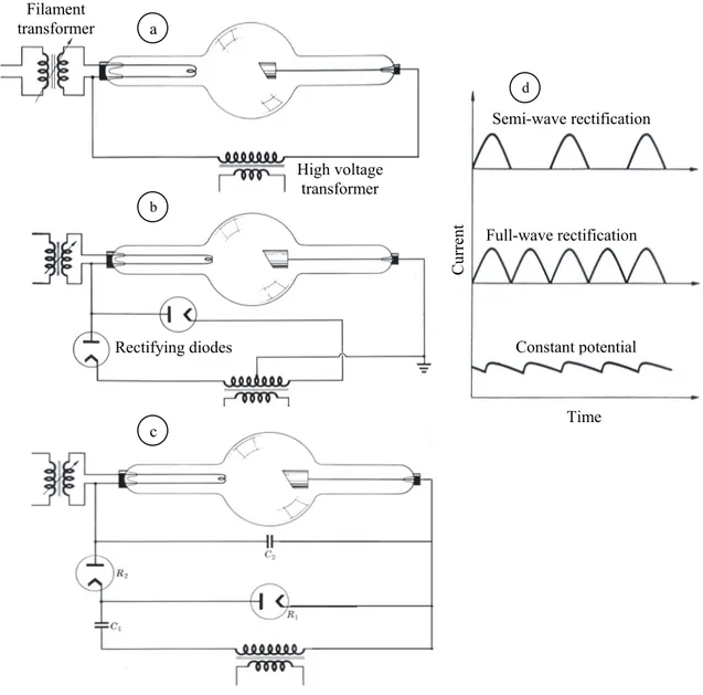
The X-ray generators based on Coolidge tube can be designed based on the necessity to have a time-constant or sinusoidal time-variable source. The semi-wave rectification uses the same tube as an ordinary diode; it is used for applications in which the source have to be intermittent, but it has the disadvantages of generating a heat surplus for long operative time and of having a reverse current that could damage the tube.
With a full-wave rectification a current with a frequency twice the semi-wave one is obtained, but the maximum current is decreased of a factor √2. A ripple circuit transforms the output into time-constant signal by introducing two capacities.
Fig. 1. 11. Different scheme of X-ray generators and relative coupled schemes: (a) semi-wave rectifying configuration, (b) full-wave, (c) at constant potential, and (d) relative current vs time trends.
Time Cu rren t Semi-wave rectification Full-wave rectification Constant potential Rectifying diodes High voltage transformer Filament transformer a b c d
1.3.2 Radioactive sources
The radioactive sources are excited nuclei, i.e. unstable atomic nuclei, that emit radiation when they attempt to become to reach a more stable state. Let’s note that currently the difference between X and γ radiation derives from their origin: the first one is generated by external interactions to the atomic nucleus, the second ones are nuclear2. For these kind of sources we should talk about γ-rays, but for the purpose of this thesis we will continue to talk about X-ray for the emitted radiation up to 120 keV. The radioactive sources are used in diffractometry to calibrate X-ray detectors due to the fact that they are very time stable and in any case they have a well known decay velocity. An advantage of this source is the spectral purity of the emission. The radioactive nuclides, that completely decay own to an electron capture, are particularly useful because the emitted radiation almost monochromatic. In this kind of decay, the atomic number of the generated nucleus is of a unit less then the initial isotope and the emitted radiation is characteristic of the generated nucleus. Most of the emitted photons are characteristic of transition in 1s orbital, because the probability to capture an electron in different orbitals is very low. Table 5 shows the main radioactive isotopes, the species generated by the decay and the energy of the produced radiation.
Table 5. Main radioactive isotopes, the element generated by the decay and the energy of the produced radiation corresponding to the transition 2p 3/2 ––> 1s.
X-rays
Radioactive nuclide Element Kα1 (keV)
37Ar Cl 2.622 51Cr V 4.952 55Fe Mn 5.898 71Ge Ga 9.251 103Pd Rh 20.214 109Cd Ag 22.16 125I Te 27.47 131Cs Xe 29.80
2 In the past the definition of X and γ radiation was based on the wavelength, with the γ rays having the shorter
A useful source is composed by different radioactive isotopes and a target material to produce a continuous emitted spectrum that superimposes to the discrete lines of radioactive sources.
1.3.3 Synchrotron radiation
When a charged particle q of energy E and mass m is accelerated in a curving path or circular orbit of radius R at constant velocity v, emits radiation. When the charged particles are accelerated at very high speed by accelerators as synchrotron, the radiation is referred as synchroton radiation Fig. 1. 12.
Fig. 1. 12. Schematic picture of a synchrotron radiation accelerator, hv indicates the emitted radiation and e− the charged particles (electrons).
The relativistic formula for radiated power P on the solid angle 4π is:
2 4 4 2 2 2 ( ) ( ) 3 v E q c c mc P R = (1.11)
where c is the light speed; replacing with the constant value, the irradiated power is: 4
0.0885E I
P
R
= (1.12)
where E is in GeV, I is the current in mA due to the charge particles and R is measured in meters. The electromagnetic radiation is confined in a beam that is tangent to orbit with an aperture angle ψ ≈ (mc2/E) (for energy of some GeV the aperture angle is about some tenth of a mrad), The
orbit of particle can be maintained only if the electromagnetic energy loss is balanced, usually by the application of a magnetic field.
The spectral distribution of the synchrotron radiation ranges from the infrared to X-rays. The parameter characteristic of a spectral distribution is the critical wavelength λc: half of the
synchrotron radiation power is radiated by photons below the critical wavelength (Fig. 1. 13). The expression of critical wavelengths is:
3 2 4 ( ) 3 c E R mc λ = π (1.13)
where E is in GeV, I is the current in mA due to the charge particles and R is in meter.
Fig. 1. 13. percentage of (a) emitted photon number and (b) radiated power as functions of λ/λc. Let’s notice that the
50% of Power and only the 9% of photons are irradiated for wavelength less λc.
λ / λc λ / λc Relative power (%) ph otons percenta ge (% )
The unchallenged advantages of synchrotron radiation, that make it an ideal tool of matter properties investigation (from atoms to solid material to biology), are:
– very high density;
– a wide continuous spectral range; – sharp angular collimation;
– limited transversal size of beam; – high polarization;
– highly regular pulse;
– easy calculation of its properties.
1.3.4 Plasma Sources
The wavelength of the emission peak from a radiant black body falls in the ultraviolet range at about 105 K and in the X-ray region between 106 K e 107 K. At this temperature the matter is in its plasma phase, i.e. a gas made of highly ionized atoms and electrons at high energy. For the plasma to reach these temperatures a laser beam is used with an intensity at least of 1012 W mm-2. The pulse duration has to be less then 1 ns to avoid the plasma to go off the beam. The emission spectrum shows lines group below the absorption energy characteristic of the 1s level and the intensity increases with the atomic number of the target Fig. 1. 14.
Fig. 1. 14. Spectrum of X-ray emission from a plasma obtained by a laser impinging on a Ti target.
1.4 X-ray detectors
In the X-ray history, the first detector was a screen covered by barium and platinum cyanide put close the Roentgen tube, that was the precursor of the X radiation photographic detector, used in crystallographic diffractometry up to day, but that show the disadvantage to be not stable. A different type of detector for this kind of radiation are gas detector, among which the ionization chamber, the proportional counter and the Geiger-Muller counter. At the opposite site there are crystal scintillators and solid-state detectors usually made of silicon.
1.4.1 Gas Detectors
When a X-ray beam pass though a gas, the photon can scatter the atoms of gas ionizing the gas and producing electron-ion couples. This kind of detectors are realized with a cylinder containing the gas and a metallic filament: between the filament and the cylinder a voltage difference is applied. Thus the charges of the generated couples are attracted by the opposite electrodes, with the difference that the ions having an higher mass are slower then electrons. The detection is based on the collection of the charges generated by the ionizing radiation. Three different type of gas detector exist differing for the voltage difference between the electrodes that gives rise to different phenomena inside the gas.
1.4.1.1 Ionization chamber
To understand the behavior of the ionization chamber, we highlight that the absorption efficiency increases with the atomic number Z of the gas. Moreover, increasing the atom density by controlling the pressure inside the chamber, the probability of interaction increases. Another fundamental parameter is the voltage difference applied between the metallic cylindrical cathode and the anodic filament: if it is zero or very low, the charges generated by a ionizing event can be recombine before reach the electrodes. If the voltage is sufficient high (100V), the charges are accelerating towards the respective electrode and produce a current that is proportional to the number of incident photons.
If the frequency of X photons is low, the detector is able measure the intensity of the X radiation and also to reveal the exciting signal in time. We notice that a X photon has energy more high then the energy necessary to generate a charged couple, thus if it is completely absorbed it
will produce n couple, where n is the ratio between its energy and the ionization energy of the gas. The intensity of the measured current strictly depends on the energy of the incident radiation.
1.4.1.2 Proportional counter
They can have different size and can contain different gases. A typical counter is made of a metallic cylinder, of diameter 2cm and length ranging between 8 to 10 cm, a central anodic filament and a lateral Berillium window of 0.13 mm thickness (Fig. 1. 15).
Fig. 1. 15. Schematic picture of a proportional counter.
The tube can be filled with Xenon at atmospheric pressure and with a small quantity of carbon dioxide or methane to avoid the discharges. When a X photon is absorbed, it generates an electron-hole pair that are accelerated by a voltage difference. If this voltage is high (> 300eV) the charge can create other couples giving rise to an avalanche phenomena. Thus the current is the sum of the charges created by photo-ionization amplified by a factor depending on gas and that is about 104 (for Xenon).
The number of charges reaching the anodes are equal to A⋅n, A is the amplification gas factor
and n the number of generated couple per absorbed photon, from which the name of proportional
counter. To increase the amplification factor some counters are filled at higher gas pressure.
X-ray Anode
1.4.1.3 Geiger-Muller counter
The Geiger-Muller counter is obsolete to detect the radiation, but it is useful like portable detector. In Fig. 1. 16 the scheme of the counter is shown: the cathode is a metallic cylinder usually made of chrome or iron of about 2 cm of diameter and 10cm of length; the anode is made of a tungsten filament of 0.7 diameter coaxial to the cylinder. The X-ray entry by the window whose material is not much absorbing, usually mica, with a thickness of about 0.013mm; the filling gas is usually Ar at 73 kPa or krypton at lwer pressure, with a little quantity of halogen species (0.4% of Cl or Br) to avoid damaging discharges. Between the anode and the window a space exist where the radiation is absorbed without contribute to detection.
Fig. 1. 16. Schematic picture of a Geiger-Muller counter
The tube is not uniformly sensitive to radiation, but a radial distance from the filament dependence exists. The part of volume that is most sensible to radiation is close to the filament length ad shown in Fig. 1. 16, thus to have the maximum efficiency the photon should hit very close to the filament but not onto it.
The detection efficiency varies with the wavelength of incident radiation: for the Cu K line it is of about 50%, while for the Mo K line it is of 10%.
An advantage of the Geiger counters is that they do not critically depend on temperature, because the linear response is limited by the time between a ionizing phenomenon and the collection of carriers. Another positive characteristic is the simplicity of its use and the low degrade also after a long operation time.
The voltage difference between the electrode is about 1.6 kV, that allows only very speed collection transition: for this reason the width of the output pulse is almost constant varying the energy of the incident photon beam. Finally the Geiger counters are able to make a qualitative measure of radiation, without any quantitative information.
Anode Cathode
X-ray
1.4.2 Solid-state Detectors 1.4.2.1 Scintillators
A scintillator counter is composed by two elements: a fluorescent crystal and a photomultiplier tube.
Fig. 1. 17. Schematic picture of a scintillator counter composed by a fluorescent crystal and a photomultiplier. The crystal is usually a sodium iodide (NaI) and it is activated by a 1% of Thallium (Tl) concentration in solid phase. A beryllium window allows the passage of X-ray onto the sealed crystal; the back of crystal enclosure is made of glass to allow the visible light to pass, while a fluid with refraction index similar to the window glass separates the crystal from the photomultiplier to reduce reflection effect. To amplify the signal a classical photomultiplier with dynodes of high secondary emission coefficient is used. The crystal is the medium to transform the incident radiation in visible light [13].
1.4.2.2 Semiconductor based detectors
The solid-state detector exploit the increase of electrical conductivity of semiconductor or semi-insulator due to the irradiation: measuring the photocurrent is equivalent to estimate the incident beam intensity. The most used solid are cadmium sulfur or silicon, but with the great drawbacks of undergoing to radiation damage for energetically high beams and low sensitivity for X-ray. Dosimeter based on single crystal diamond is not affected by these defect own to its high radiation resistance and high optical band-gap that make it sensitive to wavelength less then UV. The intrinsic germanium detectors have an absorption higher then silicon, but they show a lower energy resolution and an higher interference among output peak.
Fig. 1. 18. Efficiency of two common dosimeter based on semiconductor, Si on left and Ge on right.
1.4.2.3 Photodiodes.
The p-n silicon detectors have a wide application in dosimetry and they are well known to measure high energy electrons and photon beam. A lot of work has been performed to study their behaviour when exposed at different irradiation conditions. The main advantages in respect to the ionization chamber are:
- high efficiency, due to the low ionization energy (for silicon W = 3.6 eV); - there is not necessary a bias;
- good mechanical stability;
- small variation of the ratio between the stopping force of silicon in respect to that of water in the required energy range;
- High sensitivity for unit volume due to the high material density (for silicon: ρ = 5 × 10²²
cm-3)
The high atomic sensitivity and the low ionization energy make the semiconductor about 18000 times more sensitive than an ionization chamber of the same volume filled with air. The disadvantage of the silicon detector are.
- they are not tissue-equivalent, due its different atomic number, In particular the ionization sensitivity is different in respect to the water one when it is exposed at radiation <102 keV. In dosimetric application, this implies an alteration of the actual trend of the dose distribution in respect to depth.
- The damages due to high energy radiation, such as proton, inside the detector induce a reduction of the effective ionization volume related to a sensitivity decrease.
Energy (keV) Energy (keV)
Efficienc
y
(%
)
1.5 Photon Energy Loss in Matter
A photon passing through the matter can interact with energy loss by different physical processes depending on the radiation energyhν and on atomic number Z of material (Fig. 1. 19). At low energy (hν < 100keV) and high Z the photoelectric effect prevails (Fig. 1. 20) and all the
energy of the photon supplies the binding energy of an atomic electron to escapes from atom with a kinetics energy that, if it is larger then the work function, allow to escape from the material itself. Below 5 to 10 MeV the photon energy is larger then the binding energy of atomic electrons, the incident photon is deflected from its original path by an interaction with an atomic electron and this incoherent scattering process is dominant. This scattering of photons from charged particles was first observed by the physicist Arthur Compton in 1922, from which it takes its name Compton
scattering [14]. When the incoming photon gives part of its energy to the electron, then the
scattered photon has lower energy and according to the Planck relationship has lower frequency and longer wavelength. The wavelength change depends only upon the angle of scattering for a given target particle. Besides the Compton scattering, a coherent scattering occurs, the Rayleigh
scattering due to the oscillation induced by the electromagnetic field of radiation (Fig. 1. 20).
Fig. 1. 19. The different mechanisms of Photon Energy Loss in matter.
At higher photon energy a third process occurs: when the photon passes in the neighborough of an atomic nucleo an electron and a positron, the electron antiparticle of the same mass but opposite electrostatic charge, are created from the energy of the original photon. Due to the Einstein mass-energy equivalence (1905) the minimum mass-energy for the pair production is 1.02MeV. The pair production is the dominant process for hν>>5MeV
Fig. 1. 20. Total photon cross section in carbon, as a function of energy, showing the contributions of different processes: σp.e., atomic photo-effect (electron ejection, photon absorption); σcoherent, coherent scattering (Rayleigh
scattering atom neither ionized nor excited); σincoh, incoherent scattering (Compton scattering off an electron); κn pair
production, nuclear field; κe, pair production, electron field; σnuc, photonuclear absorption (nuclear absorption, usually
followed by emission of a neutron or other particle). The explanation of the last two processes are omitted in the discussion.
Notwithstanding the complexity and the heterogeneity of the processes occurring when the radiation pass trough the matter, it is possible to describe the interection radiation-matter by the Classical Theory of the Electromagnetic radiation.
The intensity I of a monochromatic X-rays flux passing trough a material decreases by absorption and diffusion as a function of the material thickness, d, following the Lambert’s law:
0 l
d
I =I e−μ (1.14)
where I0 is the initial intensity of radiation and μl is the absorption linear coefficient, which
depends on the atomic number of material and on the incident radiation energy.
In fact, let’s consider a section of infinitesimal thickness, dx, and unit surface (Fig. 1.21) of a
material whose density is ρ and electron density is n so that the total number of electrons in the
section of unit surface able to interact with radiation are nρ dx. The intensity decrease dI due to the
electrons interaction is:
e
dI = −I n dVσ ρ (1.15)
where σe is the scattering coefficient; the negative sign imply the decrease of intensity as the radiation goes forward
. Fig. 1. 21
The radiation intensity at depth x will be obtained by integrating the (1.15):
0 0
( ) m x mx
I x =I e−σ ρ =I e−μ (1.16)
where I0 is the initial intensity of the flux at the entry of material (x=0), σm = σen is the mass
scattering coefficient and μm = σmρ the absorption coefficient due to the scattering. As described above, the
energy loss in material is due to different processes so we can assume that the total absorption coefficient is the linear sum of different contributions:
l m C
μ =μ +μ + + (1.17) τ κ
where μm is the contribution of coherent scattering, μC is due to the Compton scattering, τ the photoelectric one and finally κ is the contribution due to the pair production.
To obtain the Lambert law, Eq.s (1.14) and (1.17), we have made the fundament hypothesis of monochromatic radiation. For a polychromatic X-ray flux, Eq. (1.17) becomes an integral function on all the spectrum with a suitable weight for the different spectrum components.
References
[1] Landwehr, Gottfried (1997). Hasse, A. ed., “Röntgen centennial: X-rays in Natural and Life Sciences”. Singapore: World Scientific. pp. 7–8
[2] D. Sheikh-Bagheri and D. W. Rogers, Med. Phys. 29, 379 (2002) [3] S. Webb S, P.M. Evans, Semin. Radiat. Oncol. 16, 193 (2006).
[4] A.A. Martinez, J.A. Gonzalez, A.K. Chung, et al, Cancer 88 425 (2000). [5] G.K. Zagars, A. Pollack, A.C. von Eschenbach, Cancer 79 1370 (1997).
[6] Mijnheer BJ. The clinical basis for dosimetric accuracy in radiotherapy. In: Radiation incidents. British Institute of Radiology, 1996; London, UK. pp. 16-20.
[7] B. Planskoy, Phys. Med. Biol., 25, 519 (1980). [8] E.A. Burgemeister Phys. Med. Biol., 26, 269 (1981).
[9] E.A. Burgemeister, W. Schouten, Radiat. Prot. Dosim., 6, 145 (1984).
[10] Röntgen, W. "Eine neue Art von Strahlen." Sitzungberichte der Physikalischen-medizinishen Gesellschaft zu Würzburg, 1985. - Translated, "On a New Kind of Rays" Nature 53, 274, 1896
[11] A. Eisntein, Annalen der Physik 17, 132–148, P. Lenard, Annalen der Physik 4, 149 (1902) [12] W.Parrish, X-Ray Analysis Papers, Centrex Publishing Co.(The Netherlands, 1965)
[13] N.G.Alexandropoulos, Y.Amemiya, U.W.Arndt, B.Buras, Measurement of Intensities [14] A. H. Compton, Phys. Rev. 21, 483; 22, 409 (1923)
[15] W.T.Sproull, X-Rays in practice, McGraw-Hill Book Company (New York, 1946)
[16] Compendium of Analytical Nomenclature, Definitive Rules, 1997 3rd ed., J. Inczedy, T. Lengyel, A. M. Ure, A. Gelencser, A. Hulanicki (Eds.), Blackwell Science, Oxford (1998).
[17] Niels Bohr, Philosophical Magazine 26 1 (1913) [18] H. G. J. Moseley, M. A. Phil. Mag. (1913), p. 1024 [19] M Green and V E Cosslett J. Phys. D 1 425 (1968) [20] H.A. Kramers, Phil. Mag. 46 836 (1923)
Chapter 2.
Physical Properties of CVD Diamond
2.1 Physical properties of diamond.
Diamond has been known for over two thousand years since its exceptional properties have been capturing the imagination of people since ancient times. Only in the 1950s it began to play an important role in the progress of technology in developed countries. It was diamond that brought a radically new level of performance to the mining industry and metallurgy. Attempts to use diamond in other areas had limited success. It was, however, generally recognized even at that time that diamond was among the most important strategic materials. With the rapid increase in the control of its synthesis, new possibilities have arisen to exploit its electrical and optical properties. Diamond has the widest electronic energy bandgap among the elemental semiconductors (5.47 eV), and one of the largest known energy gaps of all semiconductors. It has high diffusion energies for impurities and defects, and stable surfaces. The combination of light atomic mass and strong chemical bonding results in diamond having relatively high vibrational frequencies compared with other semiconductors.
Related to this, at room temperature and above, the capacity of diamond to conduct heat from an active area is unusually high. These properties should allow diamond to be used increasingly in a range of applications, from surface-mediated processes to high-power devices. Developments of the use of diamond require knowledge of a very wide range of properties. Some have been known for many years, such as the thermal expansion of diamond, which is required to make a heterogeneous structure of diamond and another material. Other properties have only been mapped out recently.
impurities but also of the disorder from the isotope content of the lattice. In yet other areas, exploiting high speed (terahertz) or small dimensions (nanometre), there is still much to learn.
X-ray diffraction measurements on natural diamonds indicate that of tetrahedrally bonded carbon atoms (sp3) that crystallizes into the diamond lattice which is a variation of the face centered cubic structure the cube edge length a0 of pure diamond, measured at room temperature with natural isotope content, is equal to 0.35671 nm. The actual value for a particular diamond will depend on its impurity level, its isotope content and its temperature.
Fig. 2. 1. Diamond lattice structure.
Diamond is the appropriate material for electronics, optoelectronics, thermal management and mechanical applications owing to excellent physical and chemical properties as:
• Highest mechanical resistance among the solids.
• Highest thermal conductivity among the materials (about 2000 W·m-1·K-1, four and five times
higher than silver and copper, respectively).
• Electrical insulator (resistivity for intrinsic diamond >1014 Ω·cm at room temperature) with
wide-bandgap semiconducting properties.
• Broadband optical transparency covering the UV (up to the wavelength of 225 nm, corresponding to its bandgap of 5.47 eV), visible, infrared, terahertz and microwave spectral ranges.
• High chemical inertness even at high temperature (up to 700 °C in oxidizing atmosphere, > 1000 °C under vacuum, under inert and reducing atmospheres).
• The wide band gap of diamond combined with its radiation hardness and high break-down field is used to realize detectors for UV radiation (being ‘solar blind’), nuclear radiation (n, α, β and γ ) and high-energy elementary particles. The former are of particular importance for radiation
and other light elements; hence, the response of a diamond detector to radiation will resemble that of human tissue. The latter takes advantage of diamond’s high radiation hardness, hence its resistance to high radiation fields as encountered in nuclear and particle physics experiments. • Biocompatibility and human tissue-equivalent behaviour (atomic number 6 respect to 6.5). • Negative electron affinity χ (down to -1.3 eV [1]) if hydrogen surface terminated, related to the
capability of emitting electrons.
• The diamond surface when hydrogen-terminated exhibits low or negative electron affinity (NEA) leads to the possible emission of low-energy (cold) electrons and hence find application as material for cold cathodes and electron field emitters. When the H-terminated diamond surface is exposed to H2O (and some other specific molecules) ‘transfer doping’ may take place and a two-dimensional p-type layer is formed under the sample surface (few nanometers) [2]-[3] that can be exploited to develop surface devices (e.g. MESFETs and diodes).
• Capability to be designed as a function that diamond has to play. The morphological, electronic and chemical properties can be tailored, depending on the application, by controlling the deposition parameters.
Fig. 2. 2. Transmission spectrum and thermal conductivity of diamond compared to other materials of interest. Charge carriers exhibit very high mobilities in the single-crystal diamond. Diamond can be doped p-type (with boron, Ea = 0.37 eV) and n-type (with nitrogen, Ea = 1.7 eV and phosphor, Ea = 0.56 eV). All these donor and acceptor levels are rather deep; hence, the RT conductivities of doped diamond are low. Native defects in diamond such as vacancies, interstitials, extended defects and combinations of different chemical dopants (co-doping effects) as well as combinations of dopants and defects may also give rise to electronic levels in the diamond band gap. Even though doping with both acceptor and donor impurities has been achieved, the doping of diamond is still
Property Diamond Silicon Carbide Silicon 3C 4H 6H
Atomic Number 6 ~10 ~10 ~10 14
Lattice structure fcc fcc hex hex Fcc
Atomic density (cm-3) *** 1.77×10²³
Density (g⋅cm-3) 3.52 3.21 3.21 3.21 2.33
Debye Temperature (K) *** 1860 1300 1200 1300 645
Vickers Hardness (kg⋅mm-2) *** 10000 1100
Young’s Modulus (GPa) *** 1050 150
Thermal Conductivity (W⋅m-1⋅K-1) *** 2200 360 370 490 112
Sound Velocity (m/s) *** 17500 8430
Band-Gap Energy (eV) 5.47 2.36 3.26 3.03 1.12
Intrinsic Electric Resistivity (Ω⋅cm) 1013-1016 3.2 × 10⁵
Dielectric Constant (εr) 5.7 9.7 9.7 9.7 11.9
Breakdown Electric Field (V⋅cm-1) 107 4 × 10⁶ 4 × 10⁶ 4 × 10⁶ 3 × 10⁵ Saturation Velocity (cm⋅s-1) 2.7 × 10⁷ 2.0 × 10⁷ 2.0 × 10⁷ 2.0 × 10⁷ 0.8 × 10⁷ Electron Mobility (cm2⋅V-1⋅s-1) 2150 600 1000 500 1500
Hole Mobility (cm2⋅V-1⋅s-1) 1700 400 115 100 600
Ionization Energy (eV) 13 8.4 8.4 8.4 3.6
Energy to remove an atom from lattice (eV) ***
80 47 47 47 28
Relative lifetime under strong irradiation (a.u.)
*** ~102 10 10 10 1
Table 2. I. Some physical parameters describing structural, phonon-related, electric and radiation-related properties for diamond, SiC and silicon. The symbol *** indicates the highest value among all the solids.
Table 2.I reports a comparison of the main physical properties among diamond and its strict relatives silicon carbide (in all its polymorph forms) and silicon, the reference material in electronics. Besides the highest Debye temperature, mechanical hardness among all the solid materials, diamond presents the peculiarity of being the most efficient thermal conductor and, if intrinsic or weakly doped, an electrical insulator at RT. This property rises a large amount of applications for thermal management, since, apart other ceramic materials (BN, AlN), which, in any case, are less efficient, is rare. This is due to the fact that thermal conductivity is always described by an electronic transport component a phonon transport component. The Fermi electron gas in metals makes predominant the electronic transport both for electrical and for thermal conduction, while phonon one is negligible. In diamond, the amount of free electrons is very low, whereas the phonon transport is the most efficient, resulting in the property described. Related to the phonon transport is the fastest propagation of sound in diamond, which makes it suitable for developing surface and bulk acoustic wave devices working at some GHz [4].
The wide bandgap of diamond causes a very high electric resistivity and allows very low leakage currents (in the order of pA or less depending on specific device structure). For detectors, this is a very important parameter that enables the possibility to develop simpler structures than p-n and Schottky junctions (i.e. development of photodiodes), as it occurs for silicon.
For application in high energy and intensity radiation beam monitoring, although it is less sensitive than silicon and silicon carbide (the energy to create an electron-hole couple is 13 eV against 8.4 and 3.6, respectively), it has a very high resistance to radiation damage, since the energy
2.2 Growth and doping.
The chemical vapour deposition (CVD) processes are the far cheaper production technique for synthetic diamond, allowing to grow it by activation of hydrogen and methane gases. Once activated, these gases provide the free radicals that chemically react among them and with the substrate. CVD allows the production of diamond in structure of films, a form compatible with electronic and opto-electronic applications. The only drawback of CVD production of diamond was that the resulting films had a polycrystalline structure (
Fig. 2. 3) if the deposition was performed on substrates made by other materials (e.g. silicon, silicon carbide, silicon nitride).
Fig. 2. 3
The polycrystalline structure takes rise from the film deposition dynamics: some nano-size diamond nuclei initially grow on the substrate becoming larger grains during the deposition (many of them are monocrystalline) [5]. When the grains are in contact, they are obliged to develop themselves along only one direction, perpendicular to substrate face [6]. Some grains are disfavoured with respect to others according to a preferential direction ruled by the flow direction of
Silicon substrate (700 – 800 °C) Silicon substrate (700 – 800 °C)
are the grain-boundaries, which present very different electrical properties with respect to the high-quality diamond grains (graphitic behaviour against electrically insulating one). A control of the overall electrical properties has been developed [7] and is operated by the control of deposition properties, but, although it is statistically satisfying enough, the resulting material has not the desirable reproducibility and homogeneity, especially if compared to single-crystal standard semiconductors as silicon. However the advantage of polycrystalline diamond films can be deposited on very large areas to form for example optical windows (Fig. 2. 4).
Fig. 2. 4
In this thesis, our attention will be uniquely focused on single-crystal diamond. In fact, during the early 2000s, a method for depositing single-crystal diamond films on pressure high-temperature (HPHT) substrates has been developed. It has allowed the development of single-crystals with very high quality, characterized by physical properties better than natural ones. Once finished the deposition process, the HPHT substrate can be separated chemically and/or by laser treatment and can be even reused for further depositions [8]. The unique drawback in single-crystal films is represented by a limited lateral size (1x1 cm2 at maximum) caused by the small size of the substrate. The homoepitaxy by chemical vapour deposition is not different from heteroepitaxy, since the substrate, held at a temperature of 600 - 800 °C, is exposed to an ionized mixture of roughly 1% hydrocarbon and 99% hydrogen gases at pressures ranging from 40 to 80 Torr.
The role of mono-atomic hydrogen, derived from the activation of molecular hydrogen, is fundamental for diamond deposition, both in its polycrystalline and monocrystalline structure. Mono-atomic hydrogen has the function of etching the thermodynamically favoured graphitic phases and prevent the closure of surface bonding of the growing film in sp2 correlation, typical of graphite. The CVD diamond growth occurs under conditions of non-equilibrium that is usually described as the super-equilibrium operated by hydrogen.
• Hot-filament assisted CVD (HF-CVD);
• Plasma assisted CVD (PA-CVD) at low (RF) or high (microwave) frequency; • DC plasma jet (DC-PJ);
• Torch or flame technique;
• CVD assisted by laser or ion bombardment.
HF-CVD and PA-CVD induced by microwaves (MW-CVD) are the commonly used techniques, whereas the other cover a small niche only inside the research sector. HF-CVD is the technique more versatile and consists in activating the process gases by refractory metal filaments at temperatures of 2200 – 2400 °C. Its advantage is the process scalability, since it allows the deposition of homogeneous thickness films on large areas (even on wafers up to 12 inches). For this reason, it is mainly used for depositing polycrystalline diamond films.
MW-CVD is the standard technique to deposit industrially and at R&D level single-crystal diamond films because, although the deposition areas are limited, it is the most “clean” and most efficient technique. It is clean since it does not need other materials inside the reactor expect from process gases and, owing to the high power density, can reach deposition rates up to 100 μm/h.
Fig. 2. 5. Left: HF-CVD reactor schematic drawing. Right: MW-CVD reactor schematic drawing.
Hot filament 2200 ÷ 2400 °C
650 ÷ 850 °C CVD Diamond H2 + CH4
Diamond is a wide bandgap semiconductor, in which electrons in the conduction band and holes in the valence band are free to move under the influence of an applied electric field. Free charge carriers can be supplied by injection through a junction, produced by the radiation or induced through doping. The concentration and motion of charge carriers in diamond under an externally applied electric field determines the electrical conductivity.
The motion of carriers is not completely free, since they are constantly scattered by lattice vibrations and defects. The wide bandgap EG of diamond (5.47 eV) induces a very low intrinsic carrier concentration at room temperature and consequently pure diamond is an excellent electrical insulator (the resistivity of intrinsic diamond may exceed 1016 Ω·cm [9]). In fact, in semiconductors the intrinsic carrier concentration ni is an exponentially decreasing function of energy bandgap that can be described by:
1/ 2 2 ( ) G E kT i C V n = N N e− , (2.1)
where NV and NC are the effective density of states of valence and conduction band, respectively. Diamond extrinsic semiconductivity can be obtained by doping. Boron is a small atom that well fits as a substitutional defect in the diamond lattice, made of small carbon atoms, and can successfully be introduced into the diamond lattice during the deposition processes. Boron is thus the most studied dopant in diamond and induces an extrinsic p-type conduction with an ionisation energy of 0.36 eV that can be observed at doping concentrations below 3 and 1019 atoms/cm3. At
very high boron concentrations the activation energy approaches zero and electric conduction becomes metallic. A room temperature resistivity of about 10−3 Ω·cm can be achieved for B concentrations above 1021 cm−3.
Diamond extrinsic n-type conductivity can be obtained by doping with phosphorus and nitrogen. Dopants in wide-band-gap semiconductors have a tendency to have higher ionisation energies than in narrow-band-gap semiconductors. In diamond this results in low activation with respect to thermal energy at room temperature (~26 meV). Phosphorus has an ionisation energy of about 0.57 eV whereas nitrogen of 1.7 eV [10]. In literature, it was reported a possible shallow n-dopant consisting in boron coupled with deuterium [11], but this attempt was not followed by other confirmations.
The lack of known shallow donors for diamond has led some researchers to conclude that its prospects for use in electronics are limited. Although this is partially true but, on the other hand, the extreme physical properties of diamond expand the capability in other directions. Conventional device structures cannot automatically be exported to diamond technology. A more creative