6 Prototyping on FPGA
6.1 Overview
This chapter describes the prototyping on the Virtex-II development board from
Memec of the Leon core featuring the I
2C/SPI interface. The development board includes a
Xilinx Virtex-II FPGA (XC2V1000-4FG456C) [21], which is clocked by an onboard
oscillator operating at 24 MHz. The hardware design has been downloaded to the FPGA via
the onboard JTAG interface. The P160 expansion module which enables further application
specific prototyping and testing has been also used.
First a presentation of the main features of the board and of the expansion module is
given, and then the design flow implemented is described with details about the synthesis
results and the mapping of the whole system.
Finally some case examples are presented showing the capture from the Digital
Oscilloscope screen of the data transmitted on the I
2C BUS.
6.2 Virtex-II™ V2MB1000 Development Board
The Virtex-II V2MB1000 Development Kit [22] provides a complete solution for
developing designs and applications based on the Xilinx Virtex-II FPGA family. The board
utilizes the 1-million gate Xilinx Virtex-II device (XC2V1000-4FG456C) in the 456
fine-pitch ball grid array package. The system board includes a 16M x 16 DDR memory, two
clock sources, RS-232 port, and additional support circuits. An LVDS interface is provided
with a 16-bit transmit and 16-bit receive port plus clock, status, and control signals for
each. For more details see the board user manual.
Figure 6-1 shows the board and its corresponding components and figure 6-2 shows
an high-level block diagram of the board.
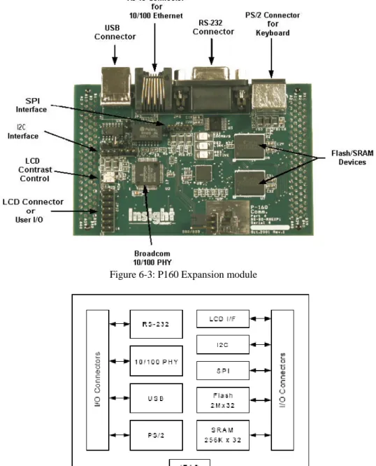
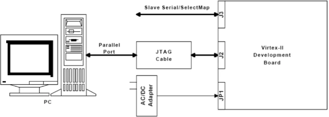
6.3 P160 expansion module
The P160 Communications Module [23] includes interfaces for USB, 10/100
Ethernet, RS-232, PS/2, Keyboard, I
2C, SPI, and an LCD display. The module also
contains both 2M x 32 Flash and 256K x 32 SRAM. Figure 6-3 shows the module and its
corresponding components, while Figure 6-4 illustrates the functional block diagram.
Figure 6-3: P160 Expansion module
6.3.1 RS232 Port
The P160 Communications Module provides a simple RS232 port. This board
utilizes the TIMAX3221 RS232 driver for driving the RD and TD signals. Figure 6-5
shows the RS232 interface.
Figure 6-5: RS232 port
6.3.2 I
2C Port
The P160 Communications Module provides one I2C port. The figure 6-6 shows the
schematic for the port
Figure 6-6: I2C port
6.3.3 FLASH and SRAM
The P160 Communications Module provides 8MB of Flash (2M x 32). Two
Toshiba TH50VSF2581 devices [24] (2M x 16 each) are used to achieve this density. In
addition to the Flash, these two devices provide 1MB of SRAM. The figure 6-7 shows the
Flash/SRAM interface on the I/O module.
Figure 6-7: Flash/SRAM interface on the I/O module
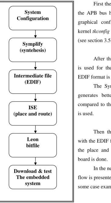
6.3.4 Design download
The Virtex-II development board supports multiple methods of configuring the
Virtex-II FPGA. The JTAG port on the Virtex-II development board can be used to directly
configure the Virtex-II FPGA, or to program the on-board XC18V04 ISP PROM as shown
in figure 6-8. Once the ISP PROM is programmed, it can be used to configure the Virtex -II
FPGA. The second has been the technique adopted for this project.
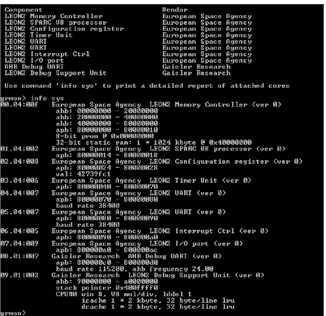
6.4 The design flow
The figure shows the design flows necessary to implement the system on the
development board:
First the Leon Core and the new IP added on
the APB bus have to be configured. To do this a
graphical configuration tool based on the linux
kernel tkconfig scripts is used to configure the model
(see section 3.5 for more details).
After this Synplicity Synplify Pro 7.3.1 [25]
is used for the synthesis. An intermediate file in
EDIF format is produced.
The Synplicity Synplify Pro synthesis tool
generates better synthesis results in most cases
compared to the synthesis results when Xilinx XST
is used.
Then the program Xilinx ISE [26] is feed
with the EDIF file produced at the previous step and
the place and route and the programming of the
board is done.
In the next sections each step of the design
flow is presented and finally the debug session and
some case examples are described.
Figure 6-9: The design flow
System
Configuration
Intermediate file
(EDIF)
ISE
(place and route)
Leon
bitfile
Download & test
The embedded
system
Symplify
(syntehesis)
6.5 The LEON configuration
The VHDL model of LEON is fully configurable to permit synthesis for different
cache sizes, multiplier units and target architectures (see section 3.5 for more details). The
boot and the initialisation of the peripherals are handled by the debug support unit. The
memory used is the SRAM present on the P160 expansion module. To can handle this
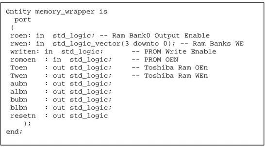
memory, a simple memory wrapper between the LEON and the memory banks has been
written; the figure 6-11 shows the VHDL entity of the wrapper. The figure 6-10 shows the
main configurations of our system:
3.2 Synthesis results Evaluation of synthesizable CPU cores
Figure 6-11: Memory wrapper entity
6.6 Synthesis results
The synthesis results presented are the total amount of lookup tables (LUT), the
number of RAMB16 cells and the number of MULT18X18 cells. In a Xilinx Virtex-II
FPGA circuit the LUT cells can implement any logic function with up to four input
variables. The smallest block RAM resource in a Xilinx Virtex-II FPGA circuit is the
RAMB16 cell, which is an 18 Kbit dual-port RAM where16 Kbit are used to store data and
2 Kbit can be used to store parity information. The MULT18X18 cell is a hardware signed
multiplier with two 18-bit inputs and one 36-bit output.
The configuration of the system is shown in figure 6-11 with a target frequency of 24 Mhz
After the synthesis with Simplify the following results have been achieved:
Table 6-1: Synthesis results.
Technology LEON2
featuring
I
2C/SPI
Number of 4-input LUTs
8710
Number of RAMB16
22
Number of MULT18x18
1
Timing 36
Mhz
e
ntity memory_wrapper is port (roen: in std_logic; -- Ram Bank0 Output Enable
rwen: in std_logic_vector(3 downto 0); -- Ram Banks WE writen: in std_logic; -- PROM Write Enable
romoen : in std_logic; -- PROM OEN
Toen : out std_logic; -- Toshiba Ram OEn Twen : out std_logic; -- Toshiba Ram WEn aubn : out std_logic;
albn : out std_logic; bubn : out std_logic; blbn : out std_logic; resetn : out std_logic );
6.7 Leon mapping
After the synthesis the Map, the Place and Route and the generation of the
programming file have been executed with the program ISE 6.2i by Xilinx [26].
Hereafter we show the pinning file for the Memec development board, the design
summary from the map report and the timing summary after the Place and Route.
Pinning of the board:
NET "clk" TNM_NET = "clk"; NET "clk" PERIOD = 41.6 ns ;
#PACE: Start of Constraints extracted by PACE from the Design NET "wdogn" LOC = "B8" ; ---> Display.2A NET "romsn<0>" LOC = "V10" ; ---> JX2.MEM_CEFn NET "resetn" LOC = "B6" ; ---> FPGA.RESETn NET "ramsn<0>" LOC = "AB12" ; ---> JX2.MEM_CE1Sn NET "toen" LOC = "V14" ; ---> JX2.MEM_OEn NET "pio<15>" LOC = "B7" ; ---> BOARD RS232.TXD NET "pio<14>" LOC = "A7" ; ---> BOARD RS232.RXD NET "pio<13>" LOC = "D7" ; ---> FPGA.PUSH1 NET "pio<12>" LOC = "A9" ; ---> BOARD USER LED NET "pio<9>" LOC = "C10" ; ---> DISPLAY.1G NET "pio<8>" LOC = "D10" ; ---> DISPLAY.1F NET "pio<7>" LOC = "F10" ; ---> DISPLAY.1E NET "pio<6>" LOC = "F9" ; ---> DISPLAY.1D NET "pio<5>" LOC = "F11" ; ---> DISPLAY.1C NET "pio<4>" LOC = "C9" ; ---> DISPLAY.1B NET "pio<3>" LOC = "D9" ; ---> DISPLAY.1A NET "pio<2>" LOC = "C4" ; ---> DIP SWITCH 3 NET "pio<1>" LOC = "A4" ; ---> DIP SWITCH 2 NET "pio<0>" LOC = "B4" ; ---> DIP SWITCH 1 NET "fl_rstn" LOC = "E18" ; ---> JX1.MEM_RESETn NET "errorn" LOC = "E9" ; ---> DISPLAY.2G NET "dsutx" LOC = "H22" ; ---> JX1.RS232_TX NET "dsurx" LOC = "H21" ; ---> JX1.RS232_RX NET "dsuen" LOC = "C5" ; ---> DIP SWITCH 4 NET "dsubre" LOC = "A6" ; ---> FPGA.PUSH2 NET "dsuact" LOC = "E7" ; ---> DISPLAY.2D NET "data<31>" LOC = "Y10" ; ---> JX2.D31 NET "data<30>" LOC = "W10" ; ---> JX2.D30 NET "data<29>" LOC = "AA9" ; ---> JX2.D29 NET "data<28>" LOC = "U12" ; ---> JX2.D28 NET "data<27>" LOC = "AA8" ; ---> JX2.D27 NET "data<26>" LOC = "U10" ; ---> JX2.D26 NET "data<25>" LOC = "U9" ; ---> JX2.D25 NET "data<24>" LOC = "AB7" ; ---> JX2.D24 NET "data<23>" LOC = "U13" ; ---> JX2.D23
NET "data<22>" LOC = "AB9" ; ---> JX2.D22 NET "data<21>" LOC = "AB8" ; ---> JX2.D21 NET "data<20>" LOC = "Y9" ; ---> JX2.D20 NET "data<19>" LOC = "U11" ; ---> JX2.D19 NET "data<18>" LOC = "W9" ; ---> JX2.D18 NET "data<17>" LOC = "AA7" ; ---> JX2.D17 NET "data<16>" LOC = "Y8" ; ---> JX2.D16 NET "data<15>" LOC = "AA14" ; ---> JX2.D15 NET "data<14>" LOC = "V13" ; ---> JX2.D14 NET "data<13>" LOC = "Y13" ; ---> JX2.D13 NET "data<12>" LOC = "AB14" ; ---> JX2.D12 NET "data<11>" LOC = "V16" ; ---> JX2.D11 NET "data<10>" LOC = "W12" ; ---> JX2.D10 NET "data<9>" LOC = "AB13" ; ---> JX2.D09 NET "data<8>" LOC = "V12" ; ---> JX2.D08 NET "data<7>" LOC = "W16" ; ---> JX2.D07 NET "data<6>" LOC = "Y17" ; ---> JX2.D06 NET "data<5>" LOC = "AA13" ; ---> JX2.D05 NET "data<4>" LOC = "Y16" ; ---> JX2.D04 NET "data<3>" LOC = "Y12" ; ---> JX2.D03 NET "data<2>" LOC = "W15" ; ---> JX2.D02 NET "data<1>" LOC = "U14" ; ---> JX2.D01 NET "data<0>" LOC = "AA12" ; ---> JX2.D00 NET "clk" LOC = "A11" ; ---> CLK.CAN1 NET "bubn" LOC = "G20" ; ---> JX1.MEM_BUBn NET "brdyn" LOC = "V6" ; ---> JX2.MEM_RY/BY NET "blbn" LOC = "H19" ; ---> JX1.MEM_BLBn NET "bexcn" LOC = "B5" ; ---> DIP SWITCH 5 NET "aubn" LOC = "G19" ; ---> JX1.MEM_AUBn NET "albn" LOC = "H20" ; ---> JX1.MEM_ALBn NET "address<24>" LOC = "W17" ; ---> JX2.A22 NET "address<23>" LOC = "AA15" ; ---> JX2.A21 NET "address<22>" LOC = "W6" ; ---> JX2.A20 NET "address<21>" LOC = "AA16" ; ---> JX2.A19 NET "address<20>" LOC = "Y6" ; ---> JX2.A18 NET "address<19>" LOC = "Y7" ; ---> JX2.A17 NET "address<18>" LOC = "W13" ; ---> JX2.A16 NET "address<17>" LOC = "W14" ; ---> JX2.A15 NET "address<16>" LOC = "AB15" ; ---> JX2.A14 NET "address<15>" LOC = "AB17" ; ---> JX2.A13 NET "address<14>" LOC = "AB16" ; ---> JX2.A12 NET "address<13>" LOC = "Y15" ; ---> JX2.A11 NET "address<12>" LOC = "Y14" ; ---> JX2.A10 NET "address<11>" LOC = "AA17" ; ---> JX2.A09 NET "address<10>" LOC = "AB18" ; ---> JX2.A08 NET "address<9>" LOC = "AB5" ; ---> JX2.A07 NET "address<8>" LOC = "V7" ; ---> JX2.A06 NET "address<7>" LOC = "AA6" ; ---> JX2.A05 NET "address<6>" LOC = "V9" ; ---> JX2.A04 NET "address<5>" LOC = "W7" ; ---> JX2.A03 NET "address<4>" LOC = "V8" ; ---> JX2.A02 NET "address<3>" LOC = "AB6" ; ---> JX2.A01 NET "address<2>" LOC = "W8" ; ---> JX2.A00 NET "twen" LOC = "AA5" ; ---> JX2.MEM_WEn NET "address<0>" LOC = "E20" ; ---> JX1.PLD_LCD_RS
Design summary from the Map report
Design Summary --- Number of errors: 0 Number of warnings: 7 Logic Utilization:Total Number Slice Registers: 2,727 out of 10,240 26% Number used as Flip Flops: 2,695
Number used as Latches: 32
Number of 4 input LUTs: 8,462 out of 10,240 82% Logic Distribution:
Number of occupied Slices: 5,011 out of 5,120 97%
Number of Slices containing only related logic: 5,011 out of 5,011 100% Number of Slices containing unrelated logic: 0 out of 5,011 0%
Total Number 4 input LUTs: 8,590 out of 10,240 83% Number used as logic: 8,462
Number used as a route-thru: 127 Number used as Shift registers: 1
Number of bonded IOBs: 131 out of 324 40% IOB Flip Flops: 141
Number of Block RAMs: 22 out of 40 55% Number of MULT18X18s: 1 out of 40 2%
Timing summary from post-place & route timing report:
Timing summary:---
Timing errors: 0 Score: 0
Constraints cover 11509544 paths, 0 nets, and 36815 connections Design statistics:
Minimum period: 30.053ns (Maximum frequency: 33.275MHz)
6.8 Debug session
Hereafter the debug session and the tools used for the debug is shown.
6.8.1 The GRMON program
GRMON [27] is a general debug monitor for
system-on-chip (SOC) designs based on
the LEON processor.
GRMON includes the following functions:
• Read/write access to all system registers and memory
• Built-in disassembler and trace buffer management
• Downloading and execution of LEON applications
• Breakpoint and watchpoint management
• Remote connection to GNU debugger (gdb)
• Support for JTAG, RS232, PCI and ethernet debug link
The monitor connects to a dedicated debug interface on the target hardware, through which
it can perform read and write cycles on the on-chip bus (AHB). The debug interface can be
of various types, in this work a serial UART is used for the debug operations.
When GRMON first connects to the target system, it scans the system to detect
which IP cores are present. If GRMON is not able to detect the plug&play area, it will
switch to a LEON2 legacy mode. A LEON2 system has a fixed set of IP cores and address
mapping, and GRMON will use an internal plug&play table that describes this
configuration. A debug driver for each recognized IP core is then initialized, and performs a
core-specific initialization sequence if required. For a memory controller, the initialization
sequence would typically consist of a memory probe operation to detect the amount of
attached RAM. For a UART, it could consist of initializing the baud rate generator and
flushing the FIFOs. After the initialization is complete, the system configuration is printed.
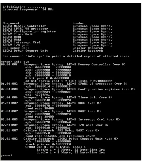
More detailed system information can be printed using the ‘info sys’ command: GRMON is
started by giving the grmon command in a terminal window. Without options, GRMON
will try to connect to the target using the serial debug link. UART1 of the host (ttyS0 or
COM1) will be used, some useful options are (refer to the the GRMON user manual for the
complete list):
grmon [options]
Options:
-stack val: Set val as stack pointer for applications, overriding the auto-detected
-u: Put UART 1 in loop-back mode, and print its output on monitor console.
-uart: device By default, GRMON communicates with the target using the first uart can be
overridden by specifying an alternative device.
The figure 6-12 shows the connection of GRMON to our target System:
Figure 6-12: GRMON connection to the system
The more common commands available regardless of loaded debug drivers are. (For
the full list of commands refer to the user manual [27])
- disas <addr> [length] disassemble memory
- echo echo string in monitor window
- help show available commands or usage for specific command
- info [drivers | libs | reg | sys] show available debug drivers, system registers or system
configuration
- load file_name load a file into target memory (elf32 or srecord)
- mem [addr] [length] display memory
- symbols show symbols or load symbols from file
- quit exit grmon
- wmem <addr> <data> write word to memory
Below is a list of some of commands provided by the LEON debug support unit
(DSU) debug driver. These commands are available when a LEON processor and
associated debug support unit is present in the target system.
-break <addr> print or add breakpoint
-cont continue execution
-dcache show data cache
-delete <bpnum> delete breakpoint(s)
-go [addr] start execution without initialization
-icache show instruction cache
-register show/set integer registers
-run [addr] reset and start execution at last entry point, or at addr
-stack [val] show/set the stack pointer
-step [n] single step one or [n] times
-watch [addr] print or add data watchpoint
6.8.2 Grmon debug session
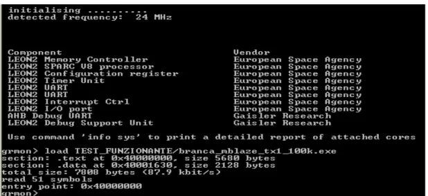
Load Applications
Figure 6-13: Load applications in GRMON
The DSU initialize the system then a program can be loaded on the system memory.
Running applications
To run the application the Run command is given. When a program reaches the end
it gives on the Uart 1 an “OK” message. The HyperTerminal connected with the Uart 1 get
this message and shows it to the user. To repeat the test “R” command is given in the
HyperTerminal, to end the test the “E” command is given on the HyperTerminal and it
turns on the LEAD on the board. A wrong insert produces the “8” number is displayed on
the 7-segment display.
Inserting breakpoints
Figure 6-15: Inserting breakpoints
To insert a breakpoint a break plus an address is given. When the run command is
given the execution stop at the breakpoint. After this the processor registers can be
displayed.
Displaying processor registers
Figure 6-16: Displaying processor registers


![Electrochemically Triggered Co-Conformational Switching in a [2]catenane Comprising a Non-Symmetric Calix[6]arene Wheel and a Two-Station Oriented Macrocycle](data:image/gif;base64,R0lGODlhAQABAIAAAP///wAAACH5BAEAAAAALAAAAAABAAEAAAICRAEAOw==)