5.1.2 EXPERIMENTAL CHARACTERIZATION IN THE P-E DOMAIN
The ferroelectric capacitor follows the dynamics (4.8) in the P-E domain. This model describes the hysteretic behavior of the ferroelectric capacitor. Before proceeding to the main point i.e. the detection of target E-fields, the material parameters (a,b,c,τ) must be determined. This has been performed by driving the device by an AC electric field at various frequencies and amplitudes, and acquiring the output voltage Vout of the Sawyer-Tower circuit. No (other) external electric field is present. The driving AC electric field must be suprathreshold, i.e. of sufficient amplitude to cause the system to sweep through its hysteresis loop or, equivalently, switch between the two stable states in the potential of Figure 4-1, on a timescale controlled by the driving period. Clearly, the driving field must be of sufficient amplitude and frequency to overcome the coercive field of the material, in a real system. Here it is important to note that, from a theoretical standpoint, one can compute the deterministic switching threshold of the dynamics (4.8) via a simple calculation of the inflexion points of the potential energy function (4.7). For a static driving field, one obtains a value of
2 / 1 3 27 4 b a . With a
time-sinusoidal driving field, the corresponding threshold value of the driving amplitude scales as the 2/3 power of the driving frequency [163]. The evaluation of the model parameters starts by identifying a, b, c and τ at the highest frequency and amplitude of the driving. The Nelder-Mead optimization algorithm [161] to minimize the squared difference between the experimental and theoretical polarizations is, then, applied; at its core is the root mean square type functional J that computes (as a percentage) the residuals between the predicted (via the model) values and the observed values of the polarization, that we seek to minimize:
100
)
(
)
ˆ
(
%
2 exp 2 exp⋅
−
=
∑
∑
P
P
P
J
(4.23)152 COUPLED FERROELECTRIC E-FIELD SENSOR
Here, Pˆ represents the estimated polarization obtained via the evaluated parameters, and Pexp represents the experimental polarization obtained by inverting (4.4). To prevent convergence of the minimization algorithm to a local minimum point in any iteration, the constraint
P
r=
(
a
/
b
)
is imposed on the parameters a and b; thisrelationship derives from the potential (4.7) representing the two stable states shown in Figure 4-1b, when no forcing field is present. Another convenience adopted for the same purpose has been to consider the parameters identified for a given frequency and amplitude of the driving voltage as initial conditions for the identification of parameters related to the driving having the same frequency but smaller amplitude and vice versa.
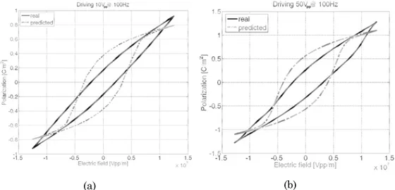
Figure 4-13 shows two examples of experimental and theoretical hysteresis loops for driving voltages having amplitudes of 10 Vpp and 50 Vpp and frequency 100 Hz, with 10 Vpp being the smallest value able to induce switching (between the two stable minima of the potential energy function) in the polarization. Table 4-1 summarizes the values of the parameters obtained through the minimization procedure for the case shown in Figure 4-13. All the model parameters have been, first, estimated with 50 Vpp @ 1 kHz driving to take into account the system dynamics, the time constant τ has been then fixed to this value while the other parameters have been used as initial values for the estimations performed in the other working conditions shown in Table 4-1. Characterization has been performed for a more spread set of voltages and frequencies, estimated parameters are not reported here for the sake of brevity. It can be observed that different values of the parameters a, b and c are obtained for different driving signal amplitudes, this being in line with earlier predictions [163] of delayed transitions in bistable systems under time-periodic external signals. The aim of the previous analysis has been the understanding of the non linear behavior of the device. This is necessary for simulation purposes and for the estimation of the material parameters which allow us to quantify the potential barrier height which constraints the device response to external perturbations.
(a)
FIGURE 4-13 Experimental and theoretical (dashed line) hysteresis loops for driving voltages having amplitudes of (
50 V
TABLE 4-1 Model parameters derived by the Nelder algorithm.
Frequency [Hz]
100
1000
(b)
Experimental and theoretical (dashed line) hysteresis loops for driving voltages having amplitudes of (a) 10 V
50 Vpp with frequency of 100 Hz.
Model parameters derived by the Nelder-Mead optimization algorithm.
Frequency [Hz] Parameter Driving 10 [V] Driving 50 [V]
a 0.745e-3 0.773e-3 b [C/m2]-2 2.580e-2 1.144e-2 c [F/m] 0.964e-9 1.255e-9 τ [s] 2.407e-6 2.407e-6 J% 19.053 18.865 Pr [C/m2] 0.17 0.26 a 1.72e-2 1.75e-2 b [C/m2]-2 7.287e-2 6.115e-2 c [F/m] 5.985e-9 8.143e-9 τ [s] 2.407e-6 2.407e-6 J% 16.132 15.063 Pr [C/m2] 0.42 0.53
Experimental and theoretical (dashed line) hysteresis loops a) 10 Vpp and (b)
Mead optimization
154
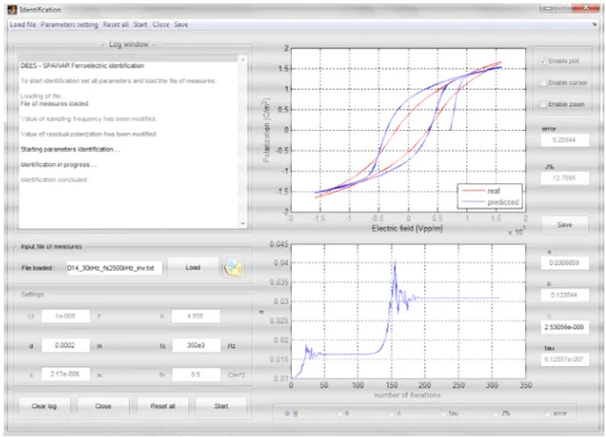
5.1.3 THE IDENTIFICATION TOOL
To the purpose to perform a model identification for the ferroelectric capacitors, a Matlab
Figure 4-14 shows the GUI of the identification tool. It permits the setting of required parameters
optimization algorithm, the sampling frequency of the experimentally acquired signal to load and some circuital and geometric parameter such as the value of the feedback capacitor, the thickness of the ferroelectric layer and its surface area. These parameters are
to convert the loaded voltage signals in the polarization and electric field signals. Moreover it shows the experimental and the predicted hysteresis (by the model) together with the estimated parameters trend.
FIGURE 4-14 GUI of the identificat
COUPLED FERROELECTRIC E-FIELD SENSOR
THE IDENTIFICATION TOOL
pose to perform a model identification for the ferroelectric capacitors, a Matlab® tool has been developed.
shows the GUI of the identification tool. It permits the setting of required parameters such as the initial conditions for the ion algorithm, the sampling frequency of the experimentally acquired signal to load and some circuital and geometric parameter such as the value of the feedback capacitor, the thickness of the ferroelectric layer and its surface area. These parameters are
to convert the loaded voltage signals in the polarization and electric Moreover it shows the experimental and the predicted hysteresis (by the model) together with the estimated parameters trend.
GUI of the identification tool.
FIELD SENSOR
pose to perform a model identification for the ferroelectric
shows the GUI of the identification tool. It permits the such as the initial conditions for the ion algorithm, the sampling frequency of the experimentally acquired signal to load and some circuital and geometric parameter such as the value of the feedback capacitor, the thickness of the ferroelectric layer and its surface area. These parameters are required to convert the loaded voltage signals in the polarization and electric Moreover it shows the experimental and the predicted hysteresis (by the model) together with the estimated parameters trend.
The core of the tool consist in three main script named: “algoritmo.m”, “funzione_errore.m”, and “risoluzione-numerica.m”, respectively.
In essence, the tool identifies a set of parameters for the analytical model (for example the parameters a, b, c, τ for the quartic potential model) chosen to represent the ferroelectric capacitor behavior by the Nelder-Mead optimization algorithm (a simplex search method).
After the loading of the Sawyer-Tower input-output signals and the plotting of the P-E hysteresis, the setting of the remnant polarization value is required. Then the identification algorithm starts by the Matlab fminsearch call: it finds the minimum of a scalar function of several variables (defined in the script “risoluzione_numerica.m”), starting at an initial estimate (the initial conditions previously defined). This is generally referred to as unconstrained nonlinear optimization. The optimization algorithm generally stops when a local minimum is reached, then it returns a set of model parameters.
The script “funzione_errore.m” defines the error function to minimize by searching an optimal set of parameters for the model defined in the third script “risoluzione_numerica.m”. At every iteration it shows the model form with the estimated parameters together with the experimental hysteresis.
5.1.4 THE BEHAVIORAL PSPICE MODEL
In order to perform numerical simulations of the system, a circuital dynamic model has been developed for the ferroelectric capacitors. Excellent agreement has been achieved between our measurements and the corresponding circuit simulations. In particular, the circuital modeling of a ferroelectric capacitor through PSPICE has been developed using a behavioral representation. The method also optimizes the process of establishing the parameter values germane to a particular hysteresis loop.
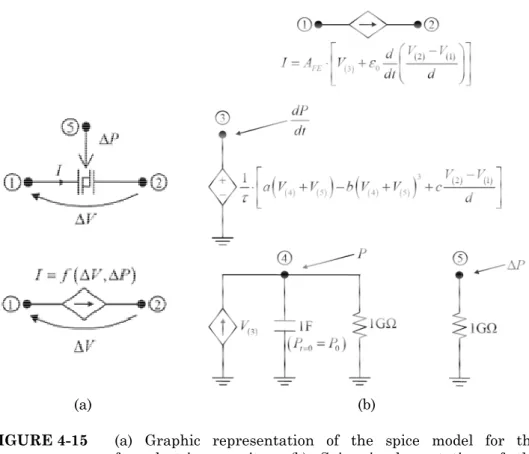
Consider the model that schematizes the capacitor as a “displacement current” generator, shown in Figure 4-15a, driven by a voltage difference that can be derived from two fundamental equations. Models underpinning the device behavior can then be realized as follows:
156
(a)
FIGURE 4-15 (a) Graphic representation of the spice model for the ferroelectric capacitor. (b) Spice implementation of the ferroelectric capacitor.
where D, P and E are having area AFE of
and electric field, respectively. Rearranging equation
Deriving equation (4.2
COUPLED FERROELECTRIC E-FIELD SENSOR
(b)
(a) Graphic representation of the spice model for the ferroelectric capacitor. (b) Spice implementation of the ferroelectric capacitor. FE A Q E P D= +
ε
0 =are the normal components to the capacitor electrodes of the vectors for displacement, electric polarization, and electric field, respectively.
Rearranging equation (4.24), it is possible to derive
)
(P 0E
A
Q= FE +
ε
4.25), an expression for the current can be obtained
+ = = dt dE dt dP A dt dQ I FE
ε
0 FIELD SENSOR(a) Graphic representation of the spice model for the ferroelectric capacitor. (b) Spice implementation of the
(4.24)
the normal components to the capacitor electrodes the vectors for displacement, electric polarization,
(4.25) ession for the current can be obtained
which is our first “constitutive” equation. In the second equation we have to take into account the dynamic behavior of the ferroelectric material cE bP aP dt dP + − = 3
τ
(4.27)where a, b, c and τ are the model parameters and E is the electric field amplitude. The value of P can be recursively evaluated by (4.27)
(
)
∫
=∫
− + = dt aP bP cE dt dt dP P 1 3τ
(4.28)A parallel plate capacitor, with a plate separation d, has been considered to evaluate the electric field amplitude E
d V V
E = (2)− (1) (4.29)
The previous model may also take into account an external perturbation, to the polarization of the ferroelectric capacitor, induced by the target field through the sensing electrode. An auxiliary input allows for introducing such a perturbation, where the voltage at this node (∆P) is expressed in units (C/m2) and summed to the actual value of P. Thus, we can write equation (4.27) as
(
)
(
)
[
a P P b P P cE]
dt dP + ∆ + − ∆ + = 1 3τ
(4.30) and as a consequence(
)
(
)
[
]
∫
+∆ − +∆ + = a P P b P P cE P 1 3τ
(4.31)Hence, equation (4.30) models the representation of the PSPICE circuit displayed in Figure 4-15b.
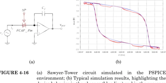
The ferroelectric capacitor model (FCAP_Pin) can be included in a Sawyer-Tower configuration as shown in Figure 4-16a. A typical simulation result is shown in Figure 4-16b. In particular, two hysteresis loops are shown to highlight the device behavior in the absence (blue line and in the presence (red line) of a target electric field having a fre-
158
(a)
FIGURE 4-16 (a) Sawyer
environment; (b) Typical simulation results, highlighti device behavior in the absence (blue line) and in the presence (red line) of a target electric field. A typical relationship between the target field and the perturbation
adopted.
quency higher than the driving voltage
5.1.5 RESPONSE TO
Equation (4.13) relates the polarization of the ferroelectric material with the target electric field via the ratio of the surface areas
charge collector and the sensing electrode. It asserts that a variation of the target electric field yields a proportional variation in the polarization state of the ferroelectric region under the s
and, hence, a variation of the output voltage of the conditioning circuit. This behavior is modeled by
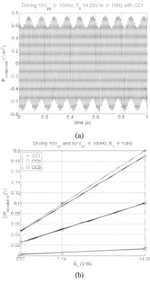
Figure 4-17a shows an example of polarization signal obtained by simulating (4.14) and (4.
voltage of 10Vpp
14.29 V/m @ 10 Hz. The target electric field produces a “modulation” of the output signal whose depth depends on the intensity of the target field itself (Figure 4
target field. Actually the “modulation” depth also depends on the area of the charge collector (considering that the
COUPLED FERROELECTRIC E-FIELD SENSOR
(b)
(a) Sawyer-Tower circuit simulated in the PSPICE environment; (b) Typical simulation results, highlighti device behavior in the absence (blue line) and in the presence (red line) of a target electric field. A typical relationship between the target field and the perturbation ∆P has been adopted.
quency higher than the driving voltage.
RESPONSE TO AN EXTERNAL E-FIELD
) relates the polarization of the ferroelectric material with the target electric field via the ratio of the surface areas
and the sensing electrode. It asserts that a variation of ric field yields a proportional variation in the polarization state of the ferroelectric region under the sensing electrode and, hence, a variation of the output voltage of the conditioning circuit.
modeled by equation (4.14).
shows an example of polarization signal obtained by and (4.13) in Matlab® for a driving (i.e. reference) pp@100 Hz and a target electric field of Hz. The target electric field produces a “modulation” of utput signal whose depth depends on the intensity of the target -17a): this is the information needed to estimate the target field. Actually the “modulation” depth also depends on the area of the charge collector (considering that the area of the sensing electrode is FIELD SENSOR
Tower circuit simulated in the PSPICE environment; (b) Typical simulation results, highlighting the device behavior in the absence (blue line) and in the presence (red line) of a target electric field. A typical relationship P has been
) relates the polarization of the ferroelectric material with the target electric field via the ratio of the surface areas of the and the sensing electrode. It asserts that a variation of ric field yields a proportional variation in the ensing electrode and, hence, a variation of the output voltage of the conditioning circuit.
shows an example of polarization signal obtained by for a driving (i.e. reference) target electric field of Hz. The target electric field produces a “modulation” of utput signal whose depth depends on the intensity of the target a): this is the information needed to estimate the target field. Actually the “modulation” depth also depends on the area of area of the sensing electrode is
FIGURE 4-17 (a) An example of the polarization signal obtained by simulating (
considering a target electric field having amplitude 14.29
(whose depth depends on the intensity of the target field) of the output signal. (b) L
peak
target electric field with three different charge collectors (CC1, CC2 and CC3); the model predicts increasing device sensitivity with increasing size of the charge collector. The solid lines are for a driving voltage of 10 V
dashed
(a)
(b)
(a) An example of the polarization signal obtained by simulating (4.13) for a driving voltage of 10
considering a target electric field having amplitude 14.29 V/m @10Hz. The electric field produces a “modulation” (whose depth depends on the intensity of the target field) of the output signal. (b) Linear interpolation of the peak-to-peak modulation amplitude for three values of the target electric field with three different charge collectors (CC1, CC2 and CC3); the model predicts increasing device sensitivity with increasing size of the charge collector. The solid lines are for a driving voltage of 10 Vpp, while the
dashed-lines are for a driving voltage of 50 Vpp.
(a) An example of the polarization signal obtained by 4.13) for a driving voltage of 10Vpp and considering a target electric field having amplitude produces a “modulation” (whose depth depends on the intensity of the target field) of inear interpolation of the peak modulation amplitude for three values of the target electric field with three different charge collectors (CC1, CC2 and CC3); the model predicts increasing device sensitivity with increasing size of the charge collector. The , while the
160 COUPLED FERROELECTRIC E-FIELD SENSOR
constant) as stated by (4.13). Figure 4-17b shows the results obtained for three different values of the target electric field and with three different charge collectors having dimensions CC1: 30 cm x 39.5 cm, CC2: 25.5 cm x 25.5 cm and CC3: 9 cm x 9 cm, respectively.
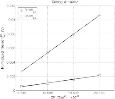
The values estimated by simulation have been interpolated by a solid line (10 Vpp) and a dashed line (50 Vpp). It can be observed that the two sets of lines in Figure 4-17b are almost superimposed, therefore no significant improvements are obtained with an increase in the driving voltage. The relevant information derivable from this is that the model predicts an increase in the device sensitivity with an increase in size of the charge collector without a significant contribution from the larger driving voltage amplitude.
A further confirmation of the expected behavior can be obtained via the PSPICE model. The simulated model circuit with the ferroelectric capacitor is shown in Figure 4-18, while an example of the output voltage signal is shown in Figure 4-19. For the purpose of investigating the effect of the polarization
∆
P, induced in the capacitance by the target E-field on the system output voltage, several simulations for different driving voltages and frequencies have been performed; in each case, we vary the amplitude and the frequency of the perturbation on the third electrode of the ferroelectric capacitance. The results confirm the expected behavior including the linear relationship between∆
P and the amplitude of the output voltage modulation, as shown in Figure 4-20 for two amplitudes of the driving voltage.FIGURE 4-18 The PSPICE model circuit with the ferroelectric capacitor.
FIGURE 4-19 An example of the output voltage signal of model in Figure 4
on the third electrode of the ferroelectric capacitance The PSPICE model circuit with the ferroelectric capacitor.
An example of the output voltage signal of the PSPICE model in Figure 4-18 showing the effect of the perturbation on the third electrode of the ferroelectric capacitance
The PSPICE model circuit with the ferroelectric capacitor.
the PSPICE showing the effect of the perturbation on the third electrode of the ferroelectric capacitance
162
FIGURE 4-20 The linearity feature relating the V with different
5.1.6 EXPERIMENTAL RESULTS
The experimental setup electrodes of 2 m x
order to avoid a direct (i.e., bypassing the charge collector) polarization of the ferroelectric. The two electrodes,
generate a uniform electric field. An AC voltage is applied to these parallel plates producing the target electric field which, in turn, produces a modulation
seen, the modulation amplitude is proportional to the target field intensity. To evaluate this modulation amplitude, the waveforms from the ST circuit have been low
The experiments involve subjecting the capacitor to a ta
having different intensities and frequencies, while also varying the dimensions of the charge collector. Specifically, the voltage (producing the target E-field across the capacitor) applied to the electrodes has been varied in amplitude from
COUPLED FERROELECTRIC E-FIELD SENSOR
The linearity feature relating the Vout amplitude modulation
with different ∆P. EXPERIMENTAL RESULTS
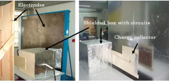
The experimental setup shown in Figure 4-21 consists of two large sheet 2 m and a guard chamber to shield the sensor in order to avoid a direct (i.e., bypassing the charge collector) polarization rroelectric. The two electrodes, separated by 1.40 m, are used to a uniform electric field. An AC voltage is applied to these parallel plates producing the target electric field which, in turn, produces a modulation (see Figure 4-22) of the output signal; as already seen, the modulation amplitude is proportional to the target field intensity. To evaluate this modulation amplitude, the waveforms from the ST circuit have been low-pass filtered.
The experiments involve subjecting the capacitor to a target E having different intensities and frequencies, while also varying the dimensions of the charge collector. Specifically, the voltage (producing field across the capacitor) applied to the electrodes has been varied in amplitude from 5 Vpp to 20 Vpp in steps of 5 Vpp and its
FIELD SENSOR
amplitude modulation
consists of two large sheet m and a guard chamber to shield the sensor in order to avoid a direct (i.e., bypassing the charge collector) polarization , are used to a uniform electric field. An AC voltage is applied to these parallel plates producing the target electric field which, in turn, signal; as already seen, the modulation amplitude is proportional to the target field intensity. To evaluate this modulation amplitude, the waveforms from
rget E-field having different intensities and frequencies, while also varying the dimensions of the charge collector. Specifically, the voltage (producing field across the capacitor) applied to the electrodes has
FIGURE 4-21 Experimental setup. The two large electrodes (2 m x 2 m each) and the guard chamber are shown in (a); the charge collector is visible in (b).
frequency varied from 5 Hz to 100 Hz. Treating the two large electrodes as a parallel plate capacitor, the target electric field amplitudes were 3.57 V/m, 7.14 V/m, 10.7 V/m and 14.29 V/m.
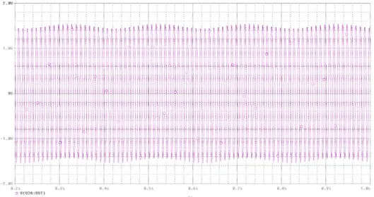
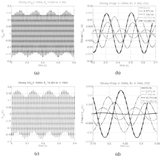
The driving voltage, applied directly to the capacitor plates, has amplitude ranging from 10 Vpp to 50 Vpp and frequencies of 100 Hz, 500 Hz and 1 kHz. All the experiments have been repeated with the three charge collectors, CC1, CC2 and CC3. Table 4-2 summarizes the settings used for the experiments. Then, as already described, the (external) target E-field induces a modulation of the output signal. Figure 4-22a and 4-22c show examples of the output signal, after removal of the mean value (this is necessary to make the low frequency components visible) obtained by a driving signal of 10 Vpp @ 100 Hz and a target electric field of 14.29 V/m @ 5 Hz and 10 Hz.
For an in depth understanding of the effect of the target E-field on the device polarization a spectral analysis of the ST output signals (correlated to the device polarization) has been carried out. Figures 4-23 (a) and (b) show the power spectral density (PSD) in the range (0 – 110 Hz) of the signals shown in Figures 4-22b and 4-22d. It is easy to detect the main peak at the frequency (100 Hz) of the driving signal and a smaller one at the frequency of the target field (5Hz in
164 COUPLED FERROELECTRIC E-FIELD SENSOR
Figure 4-23a and 10Hz in Figure 4-23b). Figures 4-23c and 4-23d show a magnification (i.e. a “zoom”) of the power spectral densities in the range (0 - 30 Hz); it is clear that a stronger target signal enhances the height of these peaks in the PSD.
The intensity of the target electric field is then estimated by low-pass filtering the output voltage signal of Sawyer-Tower circuit; examples of such signals are reported in Figures 4-22b and 4-22d.
Taking into account equations (4.4) and (4.13), a relationship between the low-pass filtered ST output signal and the external target field Ex can be considered to have the following form
β
α
∆ + = ∆ x pp out E V (4.32)Considering the peak-to-peak values of the filtered signals shown in Figure 4-21b, and repeating the experiments with three charge collectors, the results shown in Figure 4-23 have been obtained for target electric fields with frequencies of 5 Hz and 10 Hz. A linear interpolation of the experimental observations leads to the parameters (α, β) reported in Table 4-3.
TABLE 4-2 Settings used in the characterization of the device with a target electric field.
Charge collector dimensions [cm x cm] Driving amplitude [V] Driving frequency [Hz] E-field intensity [V/m] E-field frequency [Hz] CC1: 30x39.5 10 100 3.57 7.14 10.7 14.29 5 10 CC2: 25.5x25.5 CC3: 9x9
(a)
(c)
FIGURE 4-22 (a) and (c) Sawyer
voltages amplitude of 10 Vpp @ 100 Hz and a target E field of 14.29 V/m @ 5 Hz and 10 Hz respe
voltage signals from the ST circuit after low and removal of mean value.
(b)
(d)
(a) and (c) Sawyer-Tower circuit output signals for driving voltages amplitude of 10 Vpp @ 100 Hz and a target E field of 14.29 V/m @ 5 Hz and 10 Hz respectively; (b) and (d) voltage signals from the ST circuit after low-pass filtering and removal of mean value.
Tower circuit output signals for driving voltages amplitude of 10 Vpp @ 100 Hz and a target E field ctively; (b) and (d) pass filtering
166
(a)
(c)
FIGURE 4-23 Power spectral density plots of the ST output signals for the cases of a driving (i.e. reference) signal of 1
and a target electric field at 5 Hz (a) and 10 Hz (b). Zooms are given in (c) and (d). The legend on each graph shows the amplitudes of the target electric field.
It is immediately apparent that there might exist an ideal dimension (between CC1 and CC
operation of the device after a certain value of the charge collector area. Figures 4-24 have two different
peak-to-peak output voltage is shown, whereas the normalize
COUPLED FERROELECTRIC E-FIELD SENSOR
(b)
(d)
Power spectral density plots of the ST output signals for the cases of a driving (i.e. reference) signal of 10 Vpp @100 Hz and a target electric field at 5 Hz (a) and 10 Hz (b). Zooms are given in (c) and (d). The legend on each graph shows the amplitudes of the target electric field.
It is immediately apparent that there might exist an ideal dimension and CC2) for the collector, probably due to saturated operation of the device after a certain value of the charge collector area. have two different y-axes scales: on the left, the peak output voltage is shown, whereas the normalize
FIELD SENSOR
Power spectral density plots of the ST output signals for the 0 Vpp @100 Hz and a target electric field at 5 Hz (a) and 10 Hz (b). Zooms are given in (c) and (d). The legend on each graph shows the
It is immediately apparent that there might exist an ideal dimension ) for the collector, probably due to saturated operation of the device after a certain value of the charge collector area. s scales: on the left, the peak output voltage is shown, whereas the normalized (to the
energy barrier height
right axis. Note that the ratio
FIGURE 4-24 Linear interpolation of the peak
signals obtained with the various “charge collectors” and a target electric field having frequency of (a) 5 Hz and (b) 10 Hz. The energy barrier is
energy barrier height U0 =a2 /4b) filtered polarization is shown on the
right axis. Note that the ratio 1/2 0
/U
P is dimensionless.
(a)
(b)
Linear interpolation of the peak-to-peak values of the output ignals obtained with the various “charge collectors” and a target electric field having frequency of (a) 5 Hz and (b) 10 Hz. The energy barrier is U0 =5.3812e−6C/m2
) filtered polarization is shown on the
peak values of the output ignals obtained with the various “charge collectors” and a target electric field having frequency of (a) 5 Hz and (b) 10
168 COUPLED FERROELECTRIC E-FIELD SENSOR
TABLE 4-3 Parameters related to the linear interpolation indicated in (4.32). Frequency [Hz] Charge collector Parameter CC1 CC2 CC3 5
α [m/V] 7.4e-3 7.5e-3 5.6e-3 β [V] 2.0e-3 1.6e-3 2.0e-3
10 α [m/V] 5.8e-3 5.6e-3 4.8e-3
β [V] 2.4e-3 3.5e-3 2.6e-3
While the experimental results demonstrate the ability of the ferroelectric device to sense quasi-static electric fields, an actual characterization (via a measure that can be used for comparison purposes) of the performance remains to be done.
An important performance parameter is the “resolution” which defines the smallest variation of the measurand that the device can resolve. To obtain this figure of merit, it is necessary to evaluate the noise floor through an analysis of the PSD. The results, for the cases of driving voltages of 10 Vpp and 50 Vpp and two frequencies (5 Hz and 10 Hz) of the electric field and for the three charge collectors are reported in Table 4-4. We note that the best results in terms of low noise (noise floor) have been obtained with a driving voltage of 10 Vpp and a target field frequency of 10 Hz.
Finally, to conclude this section, the pending problem of demonstrating the validity of the model (4.13) is addressed. To this end, starting from the results shown in Figure 4-24, the ratio between the variation of the polarization P and the variation of the target electric field (this ratio provides a measure of the device efficiency) as a function of the ratio between the two areas S1 and S2 (recall that these are the areas of the surface of electrodes of the two capacitors shown in Figure 4-6) has been evaluated for the three charge collectors.
TABLE 4-4 Evaluation of noise floor for two frequencies of the electric field (5 Hz and 10 Hz) and two amplitudes of the driving voltage (10 Vpp and 50 Vpp) Noise floor [(V/m)/ Hz] Driving voltage @100Hz [V] E-field frequency [Hz] CC1 CC2 CC3 10 5 16 0.49 19.8 10 0.4 0.4 0.45 50 5 5.76 6.67 7.5 10 3.7 3.4 5.2
The results for the two driving signals of 10 Vpp @ 100 Hz and 50 Vpp @ 100 Hz are shown in Figure 4-24, and have been interpolated by the following relationship
2 0 1 2 1
θ
ε
θ
+ = ∆ ∆ S S E P x (4.33)where, taking into account the theoretical expressions (4.13), the coefficients θ1 and θ2 must to assume values 1 and 0 respectively.
Referring to the experimental data shown in Figure 4-24, the values for θ1 and θ2 have been derived via a linear interpolation of the two first points (before then the saturation effects observed for larger plates). The slopes of the two lines are identical, thus demonstrating the effectiveness of the charge collecting strategy even though the efficiency is lower than what is theoretically predicted (this is probably related to the non-idealities in the experimental prototype). In addition, the effect of the driving signal amplitude is apparent: as expected, the external target electric field can produce a stronger perturbation effect over a lower polarized device and therefore the 10 Vpp working condition appears to be the most suitable for the capacitors considered here.
170 COUPLED FERROELECTRIC E-FIELD SENSOR
FIGURE 4-25 The ratio between the variation of the polarization P and the variation of the target electric field (this ratio provides a measure of the device efficiency) as a function of the ratio between the two areas S1 and S2. Square symbols and star symbols are used for a driving signal of 10Vpp@100Hz and 50Vpp@100Hz, respectively. A linear interpolation is also shown as used to estimate parameters θ1 and θ2; only the
data not affected by saturation have been considered.
Put differently, the target signal is quantified through its modulation of the output waveform, this modulation will be more “visible” if the driving signal is lower; hence the ideal driving signal would have an amplitude just above what is necessary to overcome the coercive field of the material.
5.2 THE RADIANT CAPACITOR
The structure of the capacitor investigated in the previous section aims to mimic the ideal structure presented in Figure 4-4. Nevertheless it has allowed us to confirm experimentally what theory and simulations had predicted.
In the normal progression toward the best suitable configuration a milestone was the one that at the end lead us to design and to place an order to Radiant Technologies Inc. [164] for the manufacturing of the first version of an integrated ferroelectric capacitor with the desiderated structure. This capacitor (the DIEES rel.1 capacitor) will be investigated in the next section. Here the investigation of suitability of capacitors produced by Radiant will be discussed. The main objective was the survey of the technology used by the manufacturer to be ensure it was compatible with our purpose.
To this purpose we purchased from Radiant five packaged dies containing their standard parallel-plate ferroelectric capacitors. These capacitors are made by about 1600 Å of 4/30/70 PNZT and Pt/LSCO electrodes. For both the top and bottom electrodes the LSCO rests between the platinum and the PNZT surfaces. A microscope image of the die with the capacitors in the outer ring (the central part of the die hosts other test structures and it is not of interest for us) together with a schematization of the investigated capacitors are shown in Figure 4-26 (a) and (b), respectively. The size of the capacitors here investigated is 220 µm x 220 µm.
Radiant uses a 5 µm integrated process, with the possibility to yield some features on some layers down to 1 micron [165]. A schematization of the Radiant’s technology with the layers’ name is shown in Figure 4-27a while a simplified schematization of the same technology with indicated the thickness and the material composition of each layer is given in Figure 4-27b. With reference to Figure 4-27, the substrate used is a 4", 500 µ thick <100> boron doped silicon wafers with a nominal doping level of 1015 and with 5000 Angstroms (Å) of thermal silicon dioxide and a little (400 Å) titanium dioxide glue layer (TiOx barrier) under the 1500 Å thick platinum bottom electrodes (BE).
172
FIGURE 4-26 (a) A microscope image of the die with the capacitors in the outer ring (the central part of the die hosts other test structures and
schematization of the investigated capacitors. The size of the capacitor is 220µm x 220µm.
A 600 Å Lanthanum strontium cobaltate
interposed between the platinum electrode and the ferroelectri material to improve the bonding between the platinum electrode and the ferroelectric. The ferroelectric (FE) has a composition of
PNZT and a thickness of about 1600 Å. Two layers of LSCO (TO) and platinum (TE) of 600 Å and 1000 Å, respectively, a
FE to realize the top electrode of the capacitor. All the stack is then covered by a passivation layer of titanium dioxide (400 Å) plus about 2300 Å of SiO2 glass (ILD). For the sake of completeness, M1 is the electrical interconnect la
electrodes to the bond pads.
COUPLED FERROELECTRIC E-FIELD SENSOR
(a)
(b)
(a) A microscope image of the die with the capacitors in the outer ring (the central part of the die hosts other test structures and it is not of interest for us); (b) schematization of the investigated capacitors. The size of the capacitor is 220µm x 220µm.
Lanthanum strontium cobaltate oxide (LSCO) layer (BO) is interposed between the platinum electrode and the ferroelectri material to improve the bonding between the platinum electrode and the ferroelectric. The ferroelectric (FE) has a composition of
and a thickness of about 1600 Å. Two layers of LSCO (TO) and platinum (TE) of 600 Å and 1000 Å, respectively, are deposed over the FE to realize the top electrode of the capacitor. All the stack is then covered by a passivation layer of titanium dioxide (400 Å) plus about glass (ILD). For the sake of completeness, M1 is the electrical interconnect layer used to form bond pads and connect the electrodes to the bond pads. It consists of 200 Å of Cr with 5000
FIELD SENSOR
(a) A microscope image of the die with the capacitors in the outer ring (the central part of the die hosts other test it is not of interest for us); (b) A schematization of the investigated capacitors. The size of the
layer (BO) is interposed between the platinum electrode and the ferroelectric material to improve the bonding between the platinum electrode and the ferroelectric. The ferroelectric (FE) has a composition of 4/30/70 and a thickness of about 1600 Å. Two layers of LSCO (TO) and re deposed over the FE to realize the top electrode of the capacitor. All the stack is then covered by a passivation layer of titanium dioxide (400 Å) plus about glass (ILD). For the sake of completeness, M1 is the yer used to form bond pads and connect the It consists of 200 Å of Cr with 5000 Å of Au.
FIGURE 4-27 (a) A schematization of the Radiant's technology with the layers name indicated; (b) A simplified schematization same technology with indicated the thickness and the material used for each layer.
5.2.1 STRUCTURAL MODIFICATION
With the purpose to use the ferroelectric capacitor to sense electric fields exploiting our methodology a modi
obtain a third separated electrode by which to perturb the polarization state of the device
configuration together with Figure 4-28.
The modification consists in to re
release a central plate (the sensing electrode) electrically isolated from (a)
(b)
(a) A schematization of the Radiant's technology with the layers name indicated; (b) A simplified schematization same technology with indicated the thickness and the material used for each layer.
STRUCTURAL MODIFICATION
With the purpose to use the ferroelectric capacitor to sense electric fields exploiting our methodology a modification on the top elect
obtain a third separated electrode by which to perturb the polarization state of the device was needed. A schematization of the new configuration together with an example of dimensions is presented in
The modification consists in to remove a ring from the top electrode to release a central plate (the sensing electrode) electrically isolated from (a) A schematization of the Radiant's technology with the layers name indicated; (b) A simplified schematization of the same technology with indicated the thickness and the
With the purpose to use the ferroelectric capacitor to sense electric fication on the top electrode to obtain a third separated electrode by which to perturb the polarization needed. A schematization of the new dimensions is presented in
move a ring from the top electrode to release a central plate (the sensing electrode) electrically isolated from
174
the outer part of the top electrode. The sensing electrode will be linked to an external plate to collect the electric charges induced by the external target electric field.
FIGURE 4-28 Schematization of the structural modification of the top electrode of the capacitor needed to realize the sensing electrode.
FIGURE 4-29 Ferroelectric capac
after the modification by the FIB of the top electrode. (a) three modified capacitors; (b) and (c) zoom of a single capacitor. The disc in the central part of the sensing electrode is the zone in which the passivation
removed to the purpose to electrically contact the electrode. COUPLED FERROELECTRIC E-FIELD SENSOR
part of the top electrode. The sensing electrode will be linked to an external plate to collect the electric charges induced by the
xternal target electric field.
Schematization of the structural modification of the top electrode of the capacitor needed to realize the sensing electrode.
(a)
(b)
(c)
Ferroelectric capacitors produced by Radiant Technologies after the modification by the FIB of the top electrode. (a) three modified capacitors; (b) and (c) zoom of a single capacitor. The disc in the central part of the sensing electrode is the zone in which the passivation
removed to the purpose to electrically contact the electrode. FIELD SENSOR
part of the top electrode. The sensing electrode will be linked to an external plate to collect the electric charges induced by the
Schematization of the structural modification of the top electrode of the capacitor needed to realize the sensing
itors produced by Radiant Technologies after the modification by the FIB of the top electrode. (a) three modified capacitors; (b) and (c) zoom of a single capacitor. The disc in the central part of the sensing electrode is the zone in which the passivation has been removed to the purpose to electrically contact the electrode.
The removal of the ring (passivation, platinum and LSCO) from the top electrode has been performed by a Focused Ion Beam (FIB) by kind permission of STMicroelectronics in Catania and in particular by the courtesy and collaboration of Dr. La Mantia and his staff.
Figure 4-29 shows FIB images of the ferroelectric capacitors produced by Radiant Technologies after the modification of the top electrode. Figure 4-29a shows three modified capacitors while a zoom of a single capacitor is shown in Figures 4-29 (b) and (c). The disc in the central part of the sensing electrode represents the zone of the sensing electrode in which the passivation has been removed to enable us to contact the electrode.
5.2.2 EXPERIMENTAL RESULTS
To start, a wide and detailed characterization of the behavior of all the ferroelectric capacitors in the P-E domain for various amplitudes and frequencies of the driving voltage, applied between the bottom and the outer top electrodes have been carried out. The ST circuit discussed in section 3.1 has been used to convert the ferroelectric polarization in a proportional output voltage signal. The electronic implementing the ST circuit together with the DIP-28 package hosting the ferroelectric capacitors is shown in Figure 4-30. Data acquisitions have been then elaborated by the identification tool introduced in section 5.1.3 adopting even for these capacitors the dynamic model (4.8) to describe their dynamic behavior.
Figure 4-31 shows some examples of experimental P-E hysteresis (red line) for the capacitor C6 of the package 2 for three amplitudes of the driving voltage (14Vpp, 8Vpp and 5 Vpp) and two different frequencies (70 kHz and 10 kHz) together with the hysteresis predicted by the model (4.8) with the identified parameters (blu dotted line).
As an example, in Table 4-5 the parameters identified for the same capacitor for different amplitudes and frequencies of the driving voltage, are reported. Furthermore, the value of the root mean square type functional J that computes (as a percentage) the residuals between the predicted (via the model) values and the observed values of the polariza-
176 COUPLED FERROELECTRIC E-FIELD SENSOR
FIGURE 4-30 The electronic implementing the Sawyer-Tower circuit together with the DIP-28 package hosting the ferroelectric capacitors fabricated by Radiant Technologies Inc.
tion, together with the values of the error defined as the root square residuals, have been included.
Finally the value of the remnant polarizations evaluated by the experimental hysteresis are reported in the last right column.
The same procedure has been adopted for all the others capacitors and for the sake of brevity their related hysteresis and identified parameters will not reported here.
70 kHz
70 kHz
70 kHz
FIGURE 4-31 Examples of experimental P
amplitudes and two frequencies of the driving voltage together with the hysteresis predicted by the mo
with the identified parameters (blu dotted line).
Driving 14 Vpp Hz 10 kHz Driving 8 Vpp 70 kHz 10 kHz Driving 5 Vpp 70 kHz 10 kHz
Examples of experimental P-E hysteresis (red line) for three amplitudes and two frequencies of the driving voltage together with the hysteresis predicted by the mo
with the identified parameters (blu dotted line).
E hysteresis (red line) for three amplitudes and two frequencies of the driving voltage together with the hysteresis predicted by the model (4.8)
178 COUPLED FERROELECTRIC E-FIELD SENSOR
TABLE 4-5 The parameters identified for the capacitor C6 of the package 2 for different amplitudes and frequencies of the driving voltage.
Parameters Identified for the capacitor C6 of the Package 2
Frequency a b c τ J error Pr
Driving 14 Vpp
70kHz 6.269e-14 1.803e-3 6.570e-13 2.814e-11 7.936 4.955e-1 0.097 60kHz 6.317e-14 1.721e-3 6.228e-13 2.814e-11 8.651 5.397e-1 0.185 50kHz 6.003e-14 1.610e-3 5.727e-13 2.814e-11 9.232 5.748e-1 0.088 40kHz 6.809e-14 1.456e-3 5.066e-13 2.814e-11 10.007 6.198e-1 0.083 30kHz 7.589e-14 1.282e-3 4.238e-13 2.814e-11 11.159 6.798e-1 0.074 20kHz 5.871e-14 9.146e-4 3.117e-13 2.814e-11 11.215 6.941e-1 0.071 10kHz 4.898e-14 5.212e-4 1.754e-13 2.814e-11 12.279 7.589e-1 0.064
Driving 12 Vpp
70kHz 6.284e-14 1.881e-3 6.307e-13 2.814e-11 7.445 4.275e-1 0.092 60kHz 5.613e-14 1.791e-3 5.943e-13 2.814e-11 8.172 4.696e-1 0.087 50kHz 5.384e-14 1.659e-3 5.407e-13 2.814e-11 8.723 4.995e-1 0.083 40kHz 5.335e-14 1.479e-3 4.760e-13 2.814e-11 9.502 5.440e-1 0.077 30kHz 4.968e-14 1.254e-3 3.934e-13 2.814e-11 10.162 5.761e-1 0.073 20kHz 4.567e-14 9.270e-4 2.899e-13 2.814e-11 10.514 5.988e-1 0.068 10kHz 4.070e-14 5.287e-4 1.639e-13 2.814e-11 11.466 6.533e-1 0.061
Driving 10 Vpp
70kHz 6.246e-14 2.033e-3 5.933e-13 2.814e-11 8.042 4.137e-1 0.083 60kHz 5.830e-14 1.943e-3 5.568e-13 2.814e-11 8.917 4.570e-1 0.079 50kHz 5.780e-14 1.761e-3 4.996e-13 2.814e-11 9.360 4.799e-1 0.076 40kHz 5.668e-14 1.575e-3 4.377e-13 2.814e-11 10.154 5.181e-1 0.071 30kHz 5.575e-14 1.301e-3 3.598e-13 2.814e-11 10.623 5.447e-1 0.067 20kHz 5.107e-14 9.543e-4 2.615e-13 2.814e-11 10.944 5.597e-1 0.064 10kHz 4.186e-14 5.457e-4 1.490e-13 2.814e-11 11.965 6.131e-1 0.057
TABLE 4-5 (continue) The parameters identified for the capacitor C6 of the package 2 for different amplitudes and frequencies of the driving voltage.
(continue) Parameters Identified for the capacitor C6 of the Package 2
Frequency a b c τ J error Pr
Driving 8 Vpp
70kHz 6.109e-14 2.419e-3 5.452e-13 2.814e-11 9.575 4.181e-1 0.072 60kHz 5.932e-14 2.297e-3 5.079e-13 2.814e-11 10.473 4.563e-1 0.068 50kHz 5.906e-14 2.052e-3 4.504e-13 2.814e-11 10.772 4.690e-1 0.065 40kHz 6.285e-14 1.822e-3 3.920e-13 2.814e-11 11.605 5.032e-1 0.061 30kHz 7.114e-14 1.484e-3 3.197e-13 2.814e-11 12.092 5.254e-1 0.058 20kHz 7.792e-14 1.064e-3 2.297e-13 2.814e-11 12.132 5.304e-1 0.056 10kHz 8.580e-14 5.960e-4 1.301e-13 2.814e-11 13.2482 5.839e-1 0.050
Driving 5 Vpp
70kHz 9.752e-14 5.437e-3 4.653e-13 2.814e-11 13.773 3.705e-1 0.041 60kHz 9.942e-14 5.133e-3 4.265e-13 2.814e-11 14.256 3.823e-1 0.038 50kHz 1.073e-13 4.413e-3 3.734e-13 2.814e-11 14.420 3.898e-1 0.038 40kHZ 1.106e-13 3.959e-3 3.235e-13 2.814e-11 14.913 4.006e-1 0.035 30kHz 1.134e-13 3.120e-3 2.581e-13 2.814e-11 15.110 4.099e-1 0.033 20kHz 1.362e-13 2.127e-3 1.823e-13 2.814e-11 15.294 4.190e-1 0.033 10kHz 1.028e-13 1.183e-3 1.009e-13 2.814e-11 16.359 4.497e-1 0.030
With the purpose to demonstrate the possibility to exploit the ferroelectric capacitors to sense electric fields experiments with the modified capacitors have been performed applying a potential to the sensing electrode. To this aim a micro-tip has been used to contact the sensing electrode. Figure 4-32 show the setup used for the experiments and an example of the ST output voltage signal on the oscilloscope. The ferroelectric capacitor together with the conditioning electronic has been placed under the microscope with the aim to contact the sensing electrode (Figure 4-32a) by the micro-tip. Figure 4-32b shows a zoom of the ferroelectric capacitor with the tip contacting the sensing electrode obtained by a CCD camera mounted on the optics of the microscope. A voltage signal produced by a voltage generator is then applied to the
180 COUPLED FERROELECTRIC E-FIELD SENSOR
(a)
(b)
(c)
FIGURE 4-32 (a) The ferroelectric capacitor with the ST circuit under the microscope to contact the sensing electrode by a micro-tip; (b) A microscope image showing the capacitor and the tip contacting the sensing electrode; (c) An example of perturbed ST output voltage after applying a potential to the tip.