UNIVERSITÀ DI PISA
Facoltà di Ingegneria
Laurea Specialistica in Ingegneria dell’Automazione
Tesi di laurea
Candidato:
Alessio Riccomi _____________________
Relatori:
Prof. Mario Innocenti ____________________
Prof. Lorenzo Pollini ____________________
DESIGN AND INSTALLATION OF THE
AUTOMATIC SYSTEM FOR THE RRR
MEASUREMENT ON NIOBIUM
Tesi di laurea svolta presso Fermilab (Batavia, IL, U.S.A.)
Sessione di Laurea del 14/12/2006
Archivio tesi Laurea Specialistica in Ingegneria dell’Automazione: etd-11192006-025131 Anno accademico 2005/2006
RINGRAZIAMENTI
Dedico questa tesi alla mia mamma, che nei momenti di maggiore solitudine e difficolta’ ha sempre cercato di incoraggiarmi. E a mia sorella, che con il suo carattere solare e con la sua passione per le lettere, e’ sempre li’ a ricordarmi che la vita non e’ solo scienza. A loro vanno i miei ringraziamenti che vengono dal cuore.
I Professori Innocenti e Pollini, miei relatori, vorrei anche ringraziare per avermi permesso di realizzare il sogno di svolgere la mia tesi in America. Cosi’ come l’Ingegner Cristian Boffo, che mi ha dato la possibilita’ di aiutarlo in un progetto di un grande centro di ricerca come Fermilab.
ABSTRACT
This thesis describes the design and implementation of the control system for an automated setup used to measure the residual resistivity ratio (RRR) of niobium for Superconducting radio frequency (SRF) cavities. The present work has been developed at Fermilab within the Technical Division SRF materials R&D group.
Fermilab is involved in the research and development of the International Linear Collider (ILC), a project that will lead to the next generation high energy particle accelerator. The fundamental component of the ILC main linacs, which constitute the major block of the entire machine, is the SRF cavity. The cavities are made out of pure niobium which is superconducting below 9.2 K. Among others, RRR is an important parameter adopted to qualify the material used for cavity fabrication. The goal of the work reported in this thesis was to automate the new RRR measurement system designed at Fermilab in order to speed up the quality control process for the future production schedule of the project. The control system has been developed using Matlab. This work can be divided in two phases: the first one consisted in the development and implementation of the data acquisition software including an advanced user interface, which has been fully completed and tested. The second one consisted in the implementation of control algorithms aiming to the automatic temperature control during the measurement process.
SOMMARIO
Questa tesi descrive la progettazione e la realizzazione di un sistema di controllo per un apparato usato per misurare il rapporto di resistivita’ residua (RRR) del niobio per cavita’ risonanti superconduttrici (SRF). Il presente lavoro e’ stato sviluppato presso Fermilab all’interno della Technical Division, gruppo ricerca e sviluppo (R&D) materiali SRF.
Fermilab e’ coinvolto nella ricerca e nello sviluppo dell’International Linear Collider (ILC), un progetto che condurra’ alla nuova generazione di acceleratori di particelle per le alte energie. Le componenti fondamentali dell’ILC main linacs, che costituisce il maggior blocco dell’intera macchina, sono le cavita’ SRF. Queste cavita’ sono ricavate dal niobio puro, che e’ superconduttore al di sotto di 9.2 K. Fra gli altri, il RRR e’ un importante parametro adottato per qualificare il materiale usato per la fabbricazione delle cavita’. L’obbiettivo del lavoro riportato in questa tesi era quello di automatizzare il nuovo sistema per la misurazione del RRR progettato al Fermilab, al fine di velocizzare il processo di controllo della qualita’ della futura catena produttiva. Il sistema di controllo e’ stato sviluppato usando Matlab. Questo lavoro puo’ essere diviso in due fasi. La prima e’ consistita nello sviluppare e realizzare un software di acquisizione dati comprendente una interfaccia utente, che e’ stato poi completato e testato. La seconda e’ consistita nello sviluppare un algoritmo di controllo per regolare la temperatura durante il processo di misurazione.
INDEX
Ringraziamenti...1 Abstract...2 Index ...3 Figure index ...6 Table index ...8 Introduction ...91. Fermilab and the ILC...11
Introduction ...11
1.1 The big picture...11
1.1.2 The Standard Model and beyond...12
1.1.3 Understanding the Higgs boson...13
1.2 Particle Accelerators...13
1.2.1 Synchrotron ...15
1.2.2 Linear Accelerators...15
1.3 ILC Layout ...18
2. Cavities, production and processing ...21
Introduction ...21
2.1 Advantages and limitations of superconducting cavities ...21
2.1.1 Superconductivity ...22
2.2 Heat conduction in Niobium...23
2.3 Cavity Geometry...23 2.4 Cavity Fabrication ...25 2.5 Cavity Processing ...26 2.5.1 Chemistry of Niobium ...26 2.5.2 Mechanical Polishing ...26 2.5.3 Chemical Polishing...27
2.6 Comparison of BCP and EP surfaces ...29
2.7 Heat treatments ...30
2.8 High Pressure ultra pure water rinsing ...30
3. Qualifies of matierials for cavities...31
Introduction ...31
3.1 Niobium production...31
3.2 Specifications for fabrications of superconductivity cavities...31
3.2.1 RRR and purity...32
3.2.2 Mechanical behavior of high purity niobium ...33
3.3 Quality controls ...35
3.3.1 Grains dimension test ...35
3.3.2 Material isotropy test ...35
3.3.3 Characterization of the superficial layer...35
3.3.4 RRR test...37
4. RRR Measurement Set-up ...38
Introduction ...38
4.1 RRR measurement...40
4.2 Experimental Apparatus Description...41
4.2.1 Sample-holder...41
4.2.2 Insert ...42
4.2.3 Cryostat...44
4.2.5 Security and ODH ...48
4.2.6 Auxiliary systems ...48
5. Electronic hardware and drivers ...50
Introduction ...50 5.1 Electronic instruments ...51 5.1.1 Lakeshore 218...51 5.1.2 Keithley 2400 ...52 5.1.3 Keithley 2182 ...52 5.1.4 Keithley 7001 ...53
5.2 Controlled mechanical hardware ...54
5.2.1 Smart motor ...54
5.2.2 Nor-Cal Genesis valves ...54
5.3 Buses...56
5.3.1 Serial RS232 ...56
5.3.2 Trigger link cable...56
5.3.3 Gpib bus...57
5.4 National instruments pci card ...57
5.5 Dell desktop PC ...57
5.2 Drivers ...57
5.2.1 National Istruments GPIB pci card...57
5.2.2 Keithley 2400 and 2182 and the delta mode ...59
5.2.3 Keithely 7001 and scanning ...60
5.2.4 Keithley 2400 as heaters commander...60
5.2.5 Keithley 2182 and the current estimation...60
5.2.6 Lakeshore 218 and the temperature reading...60
5.2.7 Smart motor ...61 6. User interface...63 Introduction ...63 6.1 Interface structure ...64 6.1.1 Settings ...64 6.1.2. Measurements...65 6.2 Interruption issue ...67 6.2.3 Control ...68
7. Identification and control...71
Introduction ...71 7.1 Identification...71 7.1.1 Interface ...71 7.1.2 Identification strategy ...72 7.1.3 Identification toolbox ...73 7.2 Control ...76
7.2.1 First tuning in Simulink environment...76
7.2.2 Fine tuning in the real system...77
8. Measurements...78
Introduction ...78
8.1 Room temperature measurement ...78
8.2 Cold measurement ...78
9. Conclusions ...81
10. References ...82
11. Appendix ...83
11.2 Keithley 7001 scannig ...85
11.3 Step motor...85
11.4 Measurements callback function ...86
11.5 Reading temperature timer and callback function ...87
FIGURE INDEX
Fig. 1 Fermilab main building (Wilson Hall) ...9
Fig. 2 Detector ...13
Fig. 3 Fermilab’s accelerator chain ...14
Fig. 4 Fermilab Acceleration Complex (TEVATRON and Main injector)...15
Fig. 5 Linear accelerator at Fermilab...16
Fig. 6 Accelerating field ...16
Fig. 7 Accelerating field scheme ...17
Fig. 8 Cavity accelerator at Fermilab ...18
Fig. 9 Proposed ILC layout...19
Fig. 10 Underground tunnel...20
Fig. 11 Elliptical cells cavity ...23
Fig. 12 Cavity 3.9 GHz: Mid Semi Cell Fig. 13 Cavity 3.9 GHz: End Semi Cell ....24
Fig. 14 Centrifugal Barrel Polishing...27
Fig. 15 EP process: chemical reactions ...28
Fig. 16 EP facility set-up ...28
Fig. 17 Niobium surfaces after BCP etching (left) and EP etching (right) ...29
Fig. 18 Average roughness as a function of the scan length of the atomic force microscope 30 Fig. 19 Eddy current scanner at Fermilab...36
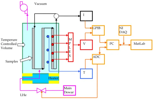
Fig. 20 Hardware system scheme ...38
Fig. 21 Experimental room drawing...39
Fig. 22 Sample-holder inside the vessel ...40
Fig. 23 Measurement scheme ...41
Fig. 24 Sample-holder ...42
Fig. 25 Insert and sample-holder ...43
Fig. 26 Vessel ...44
Fig. 27 Main Dewar...45
Fig. 28 Drawing of the main dewar...46
Fig. 29 Pump...47
Fig. 30 Drawing of the pumping system ...47
Fig. 31 Portable dewar...49
Fig. 32 Electronic instruments scheme...50
Fig. 33 Instruments cabinet ...51
Fig. 34 Lakeshore 218 ...52
Fig. 35 Keithley 2400 ...52
Fig. 36 Keithley 2182 ...53
Fig. 37 Keithley 7001 ...53
Fig. 38 Stepper motor ...54
Fig. 39 Valves...56
Fig. 40 Trigger link connection with 4-wire measurement ...59
Fig. 41 Measurement scheme with the second nanovoltmeter...60
Fig. 42 RS485 wiring diagram ...61
Fig. 43 Old RRR measurement set-up...63
Fig. 43 User interface: settings tab ...65
Fig. 44 User interface: measurements tab...66
Fig. 45 Double measurement on niobium stick...66
Fig. 46 User interface: RRR popup window ...67
Fig. 47 User interface: control tab ...69
Fig. 49 Data colltecting interface ...72
Fig. 50 Identification toolbox: primary window ...73
Fig. 51 Identification toolbox: insert data window...74
Fig. 52 Identification toolbox: process model window ...75
Fig. 53 Identification toolbox: comparison window ...76
Fig. 54 Identificated system Simulink scheme...77
Fig. 55 PID tuning Simulink scheme...77
Fig. 56 Results of room temperature measurements using Matlab interface ...78
Fig. 57 Results of cold temperature measurements using Matlab interface ...79
TABLE INDEX
INTRODUCTION
This thesis has been developed at Fermi National Accelerator Laboratory. FNAL advances the understanding of the fundamental nature of matter and energy by providing leadership and resources for qualified researchers to conduct basic research at the frontiers of high energy physics and related disciplines. Fermilab is involved in the research and development of the International Linear Collider (ILC), a project that will lead to the next generation high energy particle accelerator.
Fig. 1 Fermilab main building (Wilson Hall)
The cavities, which are the main components of the ILC main linacs are made out of pure niobium. The present work is part of the quality control process of this material. The focus of the developed work was to automate and speed up the RRR measurement process, which is one of the most important parameter adopted to qualify the material used for cavity fabrication.
The thesis is organized as follows.
The first chapter describes Fermilab and the importance of accelerator in today physics research. The main latest theories regarding matter and energy are described. An overview of nowadays accelerators is presented and linear accelerators are presented as the future of accelerators. In particular ILC details are given.
The second chapter summarizes superconductivity principles and cavities production issues. The choice of having superconductivities cavities is discussed.
The third chapter describes the main issues related to material properties such as purity, formability and grain issues. Among this the RRR is introduced.
The fourth chapter focuses on RRR and goes into details, since it’s one of the most important quality control parameter and it is the main subject of the thesis.
Hence the RRR measurement is described and details are given regarding the experimental setup from a hardware point of view.
The fifth chapter gives details on the electronic instruments that have been useful for the realization of the experiment. The structure of the set up is analyzed and the reasons of the choice of instruments are discussed. Drivers written for enabling communication between the main pc and the instruments via used buses are reported.
The sixth chapter describes the user interfaced developed using Matlab to allow an easy control of the software by the user. The software both implements the RRR measurement and a control of the system temperature needed to take measurements.
The seventh chapter describes the main approach to the identification and control strategy used to solve the problem of stabilizing the samples to the needed temperatures for measurement. In chapter eight some measurements are reported both at room temperature and cryogenic temperature to test the software.
1. FERMILAB AND THE ILC
Introduction
Fermi National Accelerator Laboratory (Fermilab) is located in Batavia, 40 miles far from Chicago, Illinois. It’s a United States national laboratory specializing in high energy particle physics. It was commissioned by the U.S. Atomic Energy Commission, under a bill signed by President Lyndon B. Johnson on November 21, 1967. On May 11, 1974, the laboratory was renamed in honor of 1938 Nobel Prize winner Enrico Fermi, one of the preeminent physicists of the atomic age. Two major components of the Standard Model of Fundamental Particles and Forces were discovered at Fermilab: the bottom quark (May-June 1977) and the top quark (February 1995). In July 2000, Fermilab experimenters announced the first direct observation of the tau neutrino, the last fundamental particle to be observed.
1.1 The big picture
Elementary particle physics has the ambitious goal of explaining the innermost building blocks of matter and the fundamental forces acting between them. Starting with the discovery of the electron, particle physicists have ventured progressively deeper into the unseen world within the atom. Their discoveries have redefined the human conception of the physical world, connecting the smallest elements of the universe to the largest, and to the earliest moments of its birth.
The masses of particles and the strength of the forces have played a key role in the evolution of the universe from the Big Bang to its present appearance in terms of galaxies, stars, black holes, chemical elements and biological systems. Discoveries in particle physics thus go to the very core of our existence.
As a consequence of the interplay of theory and experiment, in which the evolution of accelerators has played a key role, particle physics, has made enormous progress in the course of the last century. The current view is that nature is composed of two basic sets of fundamental particles: the quarks and leptons (among the leptons are electrons and neutrinos), and a set of fundamental forces that allow these to interact with each other. The "forces" themselves can be regarded as being transmitted through the exchange of particles called gauge bosons. An example of these is the photon, the quantum of light and the transmitter of the electromagnetic force we experience every day. This view is formalized by the Standard Model. The Standard Model is one of the most consistent formulations and probably the most elegant theory in the field of physics.
Nevertheless, the Standard Model theory is only an intermediate step in the formulation of a more complete theory, which will include the gravitational force. It is believed by many physicists that the four main forces present in nature (electromagnetic force, weak force, strong force and gravitational force) can be unified into one fundamental force at very high energies.
The most popular theory, which could supersede the Standard model, is Supersymmetry which in fact predicts that, at the extreme energies which were present just after the Big Bang, all of nature’s forces were combined in one single force. These split into the four forces that we know today as the universe cooled.
Our current understanding is the fruit of enormous intellectual and economic expenditure involving the whole scientific community working in diverse projects. Prominent amongst these are the high energy accelerators which reach for progressively higher energies. New technologies and materials must be developed in order to reach these higher energies and it is at this point that physicists and engineers find common ground.
The contributions of present accelerators like LEP at CERN and the Tevatron at Fermilab set the scene for the most recent and largest of these accelerators, the LHC which is about to begin
taking data at CERN and for the proposed construction of the ILC. A little further detail is needed to explain this progression.
1.1.2 The Standard Model and beyond
Nowhere have the predictions of the Standard Model found more convincing corroboration than in its ability to explain the results of collisions between the high energy protons and antiprotons or electrons and positrons accelerated and made to collide by means of accelerators. In the past thirty years, huge strides were made in understanding the interrelationships of the strong force that binds the nuclei, the electromagnetic force, and the weak force that causes radioactive decays and powers the sun.
All the three forces are now understood in terms of ‘gauge theories’ in which the symmetry of fields dictates the existence of force-carrying particles (the gauge bosons) that have one unit of spin and no mass. The forces are exerted upon the quarks and leptons, the building blocks of matter, through gauge boson exchanges. The strong force is mediated by a set of eight gluons, and the electromagnetic force by the photon. The weak force requires quite massive force carriers called the W and Z bosons to account for its short range. The three forces are distinguished by characteristic particle properties such as electric charge, to which each of the forces respond. Though the electromagnetic and weak forces seem quite different, by the laboratory experiments, it is understood now that they are in fact two aspects of a unified whole.
These ideas form the basis for the standard model, whose predictions have now been confirmed through hundreds of experimental measurements. Experiments over the past two decades using accelerators at CERN, SLAC and Fermilab discovered the W and Z bosons, demonstrated their close connection to the photon, and firmly established the unified electroweak interaction. The puzzle of the massive W and Z bosons is explained in terms of primordial weak and electromagnetic force carriers were originally mass-less, but acquire mass through an electroweak symmetry breaking mechanism. The standard model hypothesizes is that this mechanism is associated with a Higgs boson, so far undetected. This standard model Higgs boson should be discovered in experiments at sufficiently large collision energy. Although it has yet to be observed, the standard model predicts its properties precisely, its spin and internal quantum numbers; its decays to quarks, leptons, or gauge bosons; and its self-interaction. Only the Higgs boson’s mass is not specified by the theory.
Over the years the wealth of high precision studies of W, Z and photon properties, the direct observation of the massive top quark, and neutrino scattering rates have confirmed the validity of the standard model and have severely constrained possible alternatives. These studies give a range within which the Higgs boson mass should lie. From the direct searches, it is known that the Higgs boson mass is larger than about 114 GeV. The precision measurements limit the Higgs mass to less than about 200 GeV in the context of the standard model, and only somewhat larger for allowed variant models. The most likely Higgs mass is in fact just above the present experimental lower mass limit.
The proton-antiproton Tevatron Collider now operating at Fermilab could discover some of the lower mass states involved in electroweak symmetry breaking. In 2007, the LHC now under construction at CERN will obtain its first proton collisions at 14 TeV and it is therefore expected to discover a standard model Higgs boson over the full potential mass range. It should also be sensitive to new physics into the several TeV range.
The program for the future International Linear Collider (ILC) will be set in the context of the discoveries made at the LHC. However it is certain that, whatever the scenario, a detailed understanding of the results produced by the LHC will require a precision high energy electron – positron collider like the ILC.
1.1.3 Understanding the Higgs boson
The prime goal for the next round of experiments is finding the agent that gives mass to the gauge bosons, quarks and leptons. This quest offers an excellent illustration of how the LHC and the e-e- (electron-positron) International Linear Collider will magnify each other’s power. If the answer is the standard model Higgs boson, the LHC will see it. However, the backgrounds to the Higgs production process at the LHC are large, making the measurements of the couplings to quarks, quantum numbers, or Higgs self-couplings difficult. Having learnt where to look for it from the LHC, the ILC can make the Higgs boson with little background, producing it in association with only one or two additional particles, and can therefore measure the Higgs properties much more accurately.
Even if it decays into invisible particles, the Higgs can be easily seen and studied at the ILC through its recoil from a visible Z boson.
The precision measurements at the ILC are crucial to reveal the character of the Higgs boson. If the symmetry of the electroweak interaction is broken in a more complicated way than foreseen in the standard model, these same precision measurements, together with new very precise studies of the W and Z bosons and the top quark are only possible at a machine like the ILC and they will strongly constrain whatever picture corresponds to reality.
1.2 Particle Accelerators
The particle accelerator has played a key role in the evolution of nuclear and elementary particle physics. The underlying principle is very simple: charged ions or electrons are accelerated to very high velocities and made to collide with atoms contained in a stationary target or with another beam of charged particles traveling in the opposite direction. The kinetic energies imparted to the charged particles by the accelerator are large enough to fragment the particles into their constituents.
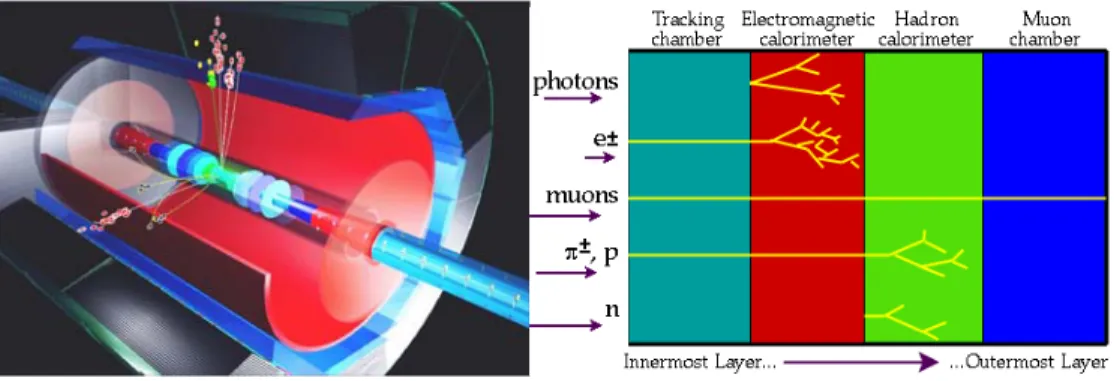
The accelerator is therefore an indispensable tool in this kind of research. Other tools are required to observe and characterize the products of the collision. These tools make up what is comprehensively known as the “detector” which is situated close to the point where the impact takes place. The most energetic collisions take place when beams traveling in opposite directions are made to collide head – on and the collider detectors which surround the impact point are giant systems composed by different types of detectors (calorimeters, scintillators, gas chambers) which are disposed in layers with the classical “onion” structure. The detector has the fundamental task of identifying the types and characteristics (e.g. the mass) of the particles generated by the impact from simultaneous measurements of energy and momentum. To this end, a combination of different detectors disposed all around the center of impact is necessary.
The following Fig. 2 illustrates schematically the structure of a typical detector.
From the very beginning, accelerator development has followed two distinct paths: circular acceleration, beginning with Lawrence’s cyclotron in 1931 and linear acceleration beginning with the Vandegraaf around the same period and the Cockroft-Walton shortly thereafter. Early linear accelerators relied on electrostatic acceleration of charged ions by means of static field whereas the cyclotron applied electrostatic fields at frequencies corresponding to the circulating ions (i.e. at radiofrequencies) to impart acceleration at each turn.
Fig. 3 Fermilab’s accelerator chain
With time and the need of ever higher energies, cyclotrons gave way to synchrotrons of ever increasing radius while linear RF accelerators were developed. For reasons outlined below, the highest energies are reached by synchrotrons when they are used to accelerate protons (or antiprotons). Because of the higher energies, these machines have a greater potential for discovery so that most important discoveries have been made employing circular synchrotrons, e.g. the discovery of the sixth and heaviest quark (the top quark) using the TEVATRON accelerator at Fermilab. This was the first synchrotron accelerator made with superconducting magnets and able to accelerate protons and antiprotons to an energy of 980 GeV, corresponding to a total center – of – mass energy of ~2 TeV in a collision between protons and antiprotons traveling in opposite directions. However, these machines have the disadvantage of producing a large quantity of unwanted particles (generally termed “background”), in addition to those of interest, because the colliding protons and antiprotons are themselves composed by more elementary particles (gluons and quarks) and because these particles interact by means of the “strong” nuclear force which is capable of generating many other fundamental particles.
On the other hand, since the electron is itself an elementary particle and it interacts by means of the weaker electromagnetic force, collisions between electrons and positrons are much cleaner. Electron-positron colliders therefore yield cleaner and more precise information but, being electrons much lighter, the radiation emission of an electron accelerated in a circular trajectory leads to much higher energy losses in synchrotrons (synchrotron radiation emission). These losses impose severe lower limits to the radius of curvature and the best way to obtain
high kinetic energies is to accelerate the electron along a straight trajectory by means of a radio frequency (RF) linear accelerator.
The basic principles underlying these two strategies to achieve particle acceleration are outlined in the following sections.
1.2.1 Synchrotron
The particles are constrained in a vacuum pipe bent into a torus, which threads a series of electromagnets, providing a field normal to the plane of the orbit. For a proton of momentum p in GeV/c and a given bending radius ρ, the field provided by the dipole magnets must have a value of B (in Tesla), where:
0.3
p= Bρ 1
The particles are accelerated once or more times per revolution by RF cavities. Both the field B and the RF frequency must increase and be synchronized with the particle velocity as it increases -hence the term of synchrotron-. Protons are usually injected from a linac source at low energy and at low field B, which increase to its maximum value over the accelerating cycle, typically lasting for a few seconds. Then the cycle begins again.
Fig. 4 Fermilab Acceleration Complex (TEVATRON and Main injector)
As mentioned above, the energy obtained with the proton synchrotron is determined by the ring radius and the maximum value of B. For conventional electromagnets using copper coils, Bmax is in the order of 1.4 T, while, if superconducting coils are used, fields of 10T or more are possible. As an example the Fermilab TEVATRON synchrotron (Fig. 4) is 1 Km in radius and it achieved an energy of 400 GeV with conventional magnets while now, using superconducting magnets, it consistently runs at 1000GeV (1TeV).
1.2.2 Linear Accelerators
The simplest accelerator is the cathodic tube of a common television. In this case the electrons are generated by a hot filament and then accelerated by the difference of potential between two charged plates (the anode and the cathode). More sophisticated electrostatic
accelerators are the Vandegraaf and the Cockroft-Walton mentioned above but the ultimate limitation of these types of accelerators arises from the maximum practical potential difference that can be held by the charged surfaces without electric discharge. Another strategy must be used to reach higher energies. The best way so far achieved to obtain this purpose is the employment of a RF linear accelerator.
Fig. 5 Linear accelerator at Fermilab
RF linear accelerators are divided in two types: • RF drift tube accelerators
• RF cavity accelerators.
Drift tube accelerators
The drift tube linear accelerators consist of an evacuated pipe containing a set of metal drift tubes, with alternate tubes attached to either side of the radiofrequency voltage. The ion source is continuous, but only those bunches of ions inside a certain time interval will be accelerated. Such ions cross the gap between successive tubes (Fig. 6) when the field is from left to right, and are inside a tube (therefore in a field free region) when the voltage change sign.
If the increase in length of each tube along the accelerator is correctly chosen, as the ion velocity increases under acceleration, the ion in a bunch receives a continuous acceleration (Fig. 7).
Typical fields obtained with such technique are a few MeV per meter of length. Such proton linacs, reaching energies in the order of 50MeV, are used as injectors for the later stages of cyclic accelerators.
Fig. 7 Accelerating field scheme
Electrons above a few MeV energy travel essentially with the velocity of light, so that after the first meter or so, an electron linac has tubes of uniform length. In practice, frequencies in the microwave range are employed and the tubes are resonant cavities of a few centimeters in dimension fed by a series of Klystron oscillators (A Klystron is a power amplifier that supplies power for the high-energy end of LINAC), which are synchronized in time to provide continuous acceleration.
Cavity accelerators
Cavity accelerators are basically composed of electromagnetic cavities resonating at a microwave frequency. This device accelerates particles using electric fields that oscillate at the same rate as the electric fields of radio waves.
Fig. 8 Cavity accelerator at Fermilab
The rapidly varying fields ensure that charged particles speeding through the cavities always feel an accelerating force. The cavity has interior surfaces which reflect a wave, usually electromagnetic, of a specific frequency. When a wave that is resonant with the cavity enters, it bounces back and forth within the cavity, with low loss. As more wave energy enters the cavity, it combines with and reinforces the standing wave, increasing its intensity. Consider the case of a charged particle moving at nearly the velocity of light. As it traverses the half-wavelength accelerating gap in half a radio-frequency period, it sees the electric field pointing in the same direction for continuous acceleration.
1.3 ILC Layout
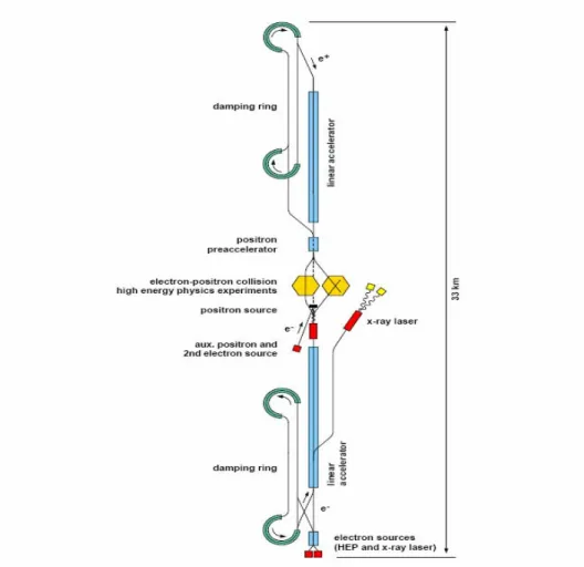
The overall layout of the ILC is shown in the following Fig. 9.
Its total length on the main linac is expected to be about 33 km depending on the achievable average gradient of the cavities. The main components are a pair of linear accelerators, one for electrons and one for positrons, pointing at each other. Each linear accelerator is constructed from about 16,000 one-meter long superconducting cavities, made in niobium and cooled by superfluid helium at -271 C. Pulsed radio frequency (1.3Ghz) electromagnetic fields are guided at 5 Hz for the duration of one millisecond into the cavities to accelerate the particles.
Fig. 9 Proposed ILC layout
Superconducting technology provides important advantages for an accelerator in general. As the power dissipation in the cavity walls is extremely small, the power transfer efficiency from the RF source to the particles is very high, thus keeping the electrical power consumption within acceptable limits (about 100MW), even for a high average beam power. The high beam power is an essential requirement to obtain a high rate of electron-positron collisions.
The electron beam for the collider is generated by a polarized laser driven source. After a short section of conventional (not superconducting) linear accelerator, the beam is accelerated to 5 GeV in superconducting structures identical to the ones used for main accelerator.
The electrons are stored in a damping ring at 5 GeV to reduce the beam size down to values needed for high luminosity operation. As the train of bunches is really long, a compression scheme is used to store the bunches in the damping ring. One of the options presently under investigation is the use of the so/called dog bone design with two 8 km straight sections, where most of the length can be accommodated inside the main accelerator tunnel. Only two 1 km loops are needed at either end. After damping, the bunch train is decompressed and injected into the main linear accelerator.
A conventional positron source cannot provide the total charge of about 5*1013 positrons per beam pulse needed for the high luminosity operation of the collider. Therefore an alternative technique has to be adopted such as the following: an intense photon beam is generated by passing the high energy electron beam through an undulator magnet placed after the main linear accelerator. Positrons are produced by directing the photons onto a thin target in which they are converted into pairs of electrons and positrons. After acceleration to 250 MeV in a normal
conducting linear accelerator the positron beam is transported to a 5 GeV superconducting accelerator and injected into the positron damping ring.
The RF power to excite the superconducting cavities is generated by ~300 klystrons per linear accelerator.
The two linear accelerators will be installed in an underground tunnel of 5.2 m diameter
(Fig. 10). [1].
2. CAVITIES, PRODUCTION AND PROCESSING
Introduction
The performances of superconducting cavities are strongly affected by the quality of their RF surface. In fact the superconducting currents flow in a surface layer which is only a few nanometers thick. This layer should be as free form defects as possible. Insufficient degreasing, variation of the grain structure and, in general, surface damage caused by the material forming process and later by the machining of the cells themselves can all degrade the cavity performance. These effects manifest themselves in two major limiting phenomena: field emission and multipacting.
Multipacting is a phenomenon of resonant electron multiplication. In high energy particle accelerators, it leads to the build – up of a large number of electrons which eventually form an electron avalanche, leading to power losses and heating of the walls, so that it becomes impossible to increase the cavity fields by raising the incident power.
This effect can seriously limit the performance of the cavity. Therefore a lot of precautions are taken to avoid particle contamination and generally to improve the cavity performances. A great number of studies and the experience have demonstrated that the RF performance of a cavity in the superconductive state is increased by the employment of cavities with a particular geometry and by the polishing of the cavity surface. The shape has been largely optimized in the past fifteen years, mostly thanks to the availability of powerful tri-dimensional simulation codes. Right now the Tesla, re-entrant and low loss shapes are much more effective in reducing multipacting with respect to the original pill box. Nevertheless, multipacting can still happen in particular areas of the cavity, as was recently was discovered in several high order modes couplers. The introduction of chemical polishing and high pressure rinse additionally reduced the possibility of multipacting and field emission.
Great care is taken during cavity processing and assembly to keep the RF surface as clean as possible; for this reason all the assembly operations are performed in class 10 clean rooms. At the moment many laboratories are pursuing a strong R&D program to increase the average accelerating gradient of the cavities and, to this end, they are experimenting several new techniques for obtaining a smooth and clean RF surface. It has been found that a gradient of 25 MV/m may be consistently achieved if the following typical processing recipe is adopted:
1. External chemical polishing with a removal of a 30 μm surface layer to remove impurities, increases the thermal heat exchange with superfluid helium and limits furnace contamination during heat treatments.
2. Internal chemical polishing with a removal of 150 μm to eliminate the surface damaged layer created during the cavity fabrication process.
3. Annealing heat treatment at 750-800 °C to allow for hydrogen degassing.
4. Internal chemical polishing with a removal of 50 μm to eliminate the contaminants surfaced during the heat treatment.
5. Low temperature bake at 120 °C to remove Q-drop (physical underling phenomenon still under investigation, but basically a drop of the quality factor Q which is discussed below). 6. High pressure rinse at 100 bar of the RF surface to remove any loose particles.
7. Assembly in clean room.
2.1 Advantages and limitations of superconducting cavities
The fundamental advantage of superconducting cavities with respect to the normal conducting ones is the extremely low surface resistance and the high quality factors. Superconducting cavities typically work in the range between 4.5 and 2K. In this range the BCS
(later explained) and residual resistance are the two dominating components and can be as low as 10 nOhms, at least five order of magnitude lower than the copper used for normal conducting cavities. In addition to this, the intrinsic quality factor, Q, for high performing cavities can be as high as 1011. The quality factor is the ratio between the energy stored in the cavity and the one dissipated during one RF period, thus offering a measure of the number of oscillations a resonator will go through before dissipating its stored energy. Furthermore, despite of the low efficiency of the helium refrigeration system there are considerable savings in primary electric power to be had by choosing superconducting RF cavities instead of the equivalent normal conducting ones.
The physical limitation of SC resonators is given by fact that, in order to operate properly, the superconductor must be kept within the vortex free state corresponding roughly to the Meissner state. To be more precise the working area is more extended with respect to the Meissner since the vortexes need some time to generate and penetrate the surface of the material and this time is a few orders of magnitude longer than the RF period. For this reason the RF critical field or superheating critical field is much higher than the regular first critical field under DC conditions. The surface field limitations translate, with the present ILC cavity shape, into an average accelerating gradient limit of ~60 MV/m.
In reality the theoretical limit is very hard to reach since many factors can lower the real operating gradient of the cavity. Even the Q versus accelerating gradient curve, in theory, should be a flat line that stops with a vertical drop corresponding to a quench, in reality the presence of field emission, multipacting and the formation of hotspots affect the slope of the curve in many different ways.
2.1.1 Superconductivity
The resistance of a metallic conductor decreases gradually as the temperature is lowered. However, in ordinary conductors such as copper and silver, impurities and other defects impose a lower limit. Even near absolute zero a real sample of copper shows a non-zero resistance.
The resistance of a superconductor drops to zero when the material is cooled below its critical temperature, typically 20 K or less. An electrical current flowing in a loop of superconducting wire will persist indefinitely with no power source. Like ferromagnetism. Superconductivity is a quantum mechanical phenomenon. It cannot be understood simply as the idealization of perfect conductivity in classical physics.
An accredited theory is the J. Bardeen, L. N. Cooper, and J. R. Schrieffer one. BCS theory views superconductivity as a macroscopic quantum mechanical effect. It proposes that electrons with opposite spin can become paired, forming Cooper pairs. In many superconductors, the attractive interaction between electrons (necessary for pairing) is brought about indirectly by the interaction between the electrons and the vibrating crystal lattice (the phonons). An electron moving through a conductor will attract nearby positive charges in the lattice. This deformation of the lattice causes another electron, with opposite "spin", to move into the region of higher positive charge density. The two electrons are then held together with a certain binding energy. If this binding energy is higher than the energy provided by kicks from oscillating atoms in the conductor (which is true at low temperatures), then the electron pair will stick together and resist all kicks, thus not experiencing resistance.
Basically, it’s possible to distinguish two types of superconductor materials: 1. type-I superconductor,
2. type-II superconductor.
In comparison to the (theoretically) sharp transition of a type-I superconductor at its single critical temperature, a type-II superconductor has two critical temperatures. Above the lower temperature Tc1, magnetic flux from external fields is no longer completely expelled, and the
superconductor exists in a mixed state. Above the higher temperature Tc2, the superconductivity
dependent on the strength of the applied field. type-II superconductors tend to be made of metal alloys, whereas type-I superconductors tend to be made of pure metals.
The existing large scale applications for superconductors are magnets and accelerating cavities. A common requirement is a high critical temperature, but there are distinct differences concerning the critical magnetic field. In magnets operated with a dc or a low-frequency ac current, type I superconductors are required, with high upper critical fields (15-20 T) and strong flux pinning in order to achieve high current density; such properties are only offered by alloys like niobium-titanium or niobium-tin. In microwave applications the limit is essentially set by the thermodynamic critical field, which is well below 1 T for all known superconductors. Strong flux pinning is undesirable as it is coupled with losses due to hysteresis. Hence a type II superconductor must be used. Pure niobium is the best candidate, although its critical temperature Tc is only 9.2 K, and the thermodynamic critical field about 200mT. Niobium-tin (Nb3Sn) with a critical temperature of 18K looks more favorable at first sight, however the gradients achieved in Nb3Sn coated niobium cavities were always below 15 MV/m, probably due to grain boundary effects in the Nb3Sn layer. [2].
2.2 Heat conduction in Niobium
The heat produced by the RF field at the inner cavity surface has to be guided through the cavity wall to the super fluid helium bath. Two factors characterize the heat flow: the thermal conductivity of the bulk niobium and the temperature drop at the niobium-helium interface known as Kapitza resistance. For niobium with a residual resistivity ratio (RRR is defined as the ratio of resistivity at room temperature and at 4.2 K and is a qualitative parameter to identify the purity and the thermal properties of the material) of300, the two contributions to the temperature rise at inner cavity surface are about equal. The thermal conductivity of niobium at cryogenic temperatures scales approximately with the RRR as:
[
]
(4.2 ) 0.25K RRR W mK/
λ ≈ 2
However, λ is strongly temperature dependent and drops by about 1 order of magnitude when lowering the temperature to 2 K.
2.3 Cavity Geometry
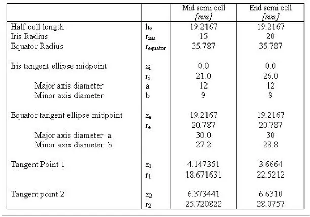
For practical application the accelerating resonators are made out of multiple cells. This solution allows one to maximize the active length of the linac and at the same time to minimize the number of power couplers, high order mode (HOM) couplers and bolted flanges. However the cell number is limited by several factors such as the difficulty to reach the proper field flatness and the power limitation of the main coupler. Given the performance of the present hardware, ILC cavities have 9 cells as illustrated in Fig. 11.
The cell shape depends on several factors of which the following are the most fundamental: • A spherical contour near the equator for low sensitivity to multipacting.
Fig. 12 Cavity 3.9 GHz: Mid Semi Cell Fig. 13 Cavity 3.9 GHz: End Semi Cell
• A large iris radius to reduce wake field effects.
• The axial dimension is determined by the inversion of the electric field within the time a relativistic particle travels from one cell to the next. The separation between two irises is therefore c/(2f).
The contour of a 3.9 GHz cavity half-cell is shown in Fig. 12. The half-cells at the end of the 9-cell resonator (Fig. 12) is slightly different shape to ensure equal electro-magnetic field amplitudes in all 9 cells.
Table 1 Cavity cell profile
2.4 Cavity Fabrication
In the early days lead was used to fabricate superconducting RF cavities and later it was substituted by niobium, which presents better superconducting properties. In particular the Meissner phase in niobium extends up to 120 mT allowing considerably high electric fields to be reached on the surface of the cavity. Nowadays there is a strong R&D effort investigating the possibility of using high temperature superconductors such as MgB2 for cavity fabrication, but niobium still remains the only material currently suitable for near future applications in accelerator technology.
There are several techniques utilized for the fabrication of elliptical cavities, which can be classified in two main categories: bulk niobium formation and thin film deposition.
The most common technology involves the formation of cavities from bulk niobium. The material in sheets can be shaped by deep drawing or spinning, while tubes can be hydroformed. Hydroforming and spinning allow formation of a full 9-cells cavity starting from a single precursor. Deep drawing is used to form half-cells that later are electron beam welded to create dumb-bells and finally the full 9-cells cavity. In The deep drawing fabrication process is described in a little more detail below.
The dies for deep drawing are typically made from a high yield strength aluminum alloy. To achieve the small curvature required at the iris an additional step of coining is added between two separate deep drawing stages.
After the forming process the half-cells are machined at the iris and equator. At the iris the half-cells are cut to the specified length while at the equator an extra length of 1 mm is left to retain the possibility of a precise length trimming of the dumb-bells after frequency measurements.
The accuracy of the shape is checked by sandwiching the half-cells between two metal plates and by measuring their resonant frequency.
The half-cells are then thoroughly cleaned by ultrasonic degreasing, 20 μm chemical etched at the equator in the weld preparation area and they are then rinsed using ultra pure water. Two half-cells are then joined at the iris with an electron beam welding process to form a dumb-bell. The electron beam welding is usually performed from the inside to ensure a smooth weld seam at the location of the highest electric field in the resonator. Since niobium is a strong getter material for oxygen it is important to carry out the electron beam welding in high vacuum.
Afterwards, frequency measurements are performed on the dumb-bells to determine the correct amount of trimming at the equators. A visual inspection followed by a 30um etch of the equator area allow finding of possible defects. If defects are discovered as a result of foreign material imprints from previous fabrication steps, they are removed by grinding. After the inspection and proper cleaning eight dumb bells and two beam-pipe sections with attached end half-cells are stacked in a precise fixture to carry out the equator welds, which are done from the outside. At this point the full cavity is fabricated and the surface processing starts.
2.5 Cavity Processing
The surface processing of a superconducting cavity is rather complex and involves several steps. Since a golden recipe has not yet been identified and since some of the steps are only necessary for very high gradients, many technologies, alternative to each other, are employed. Essentially the basic recipe includes large material removal, annealing, small material removal and high pressure rinsing. The material removal can be performed utilizing three methods: buffered chemical polishing (BCP), electropolishing (EP) and centrifugal barrel polishing (CBP). Each of these techniques has advantages and disadvantages that will be discussed below.
2.5.1 Chemistry of Niobium
Talantum with a typical concentration of 500 ppm is the most common metallic impurity in high RRR niobium. Among the interstitially dissolved impurities, oxygen is dominant due to the high affinity of Nb to it above 200 C. Distribution of oxygen in the superficial layer of the material seems to be responsible of the Q-drop phenomenon at high gradients.
A natural Nb2O5 layer with a thickness of about 5 nm is present on the niobium surface. Below this natural layer other oxides can be found. Nb2O5 has a particular structure, able to accommodate many stechiometry defects.
2.5.2 Mechanical Polishing
Centrifugal barrel polishing (CBP), also called tumbling, is a common technique used in industry for surface finishing. A layer of niobium can be removed from the surface of cavities by the friction of thin grains against the walls. CBP was introduced into cavity processing by DESY and KEK. This procedure involves filling up the cavity by grinding stones and water and rotating the cavity at high speed for several hours (Fig. 14). The standard KEK recipe is divided in 4 steps. During each step the shape and the material of the grinding agent is changed so as to reach a smooth surface. At the end of a successful procedure the weld seam at the equator is hardly visible. Since the grinding process produces a considerable amount of heat, some concern has risen about the possibility of driving large amounts of hydrogen into the material. Although the annealing process should take care of eliminating hydrogen, several studies have been performed with the goal of eliminating water from the process thus reducing the possibility of hydrogen adsorption.
CBP prior to wet chemistry has many advantages. One of them is that it prepares the surface of the cavity for wet chemistry by removing the worst defects such as scratches and by making the surface more uniform. In addition, by substituting the large material removal step, usually performed by BCP or EP, CBP leads to an overall reduction of the environmental impact of the
cavity fabrication process reducing the amount of used acid. Finally CBP is well matched with further chemical processes in terms of field flatness preservation. In reality, due to the larger centrifugal force, CBP is more effective at the cavity equator while the chemical processing is more effective at the iris where the fluid velocity is higher. As a result the combination of the two techniques allows for more uniform material removal over the entire cell.
Fig. 14 Centrifugal Barrel Polishing
2.5.3 Chemical Polishing
NB2O5 is a very stable oxide that can be dissolved only by hydrofluoric acid. HF is in fact the essential ingredient used in both the chemical etching techniques used in niobium cavity fabrication and in electropolishing (EP) and buffered chemical polishing (BCP).
Polishing the niobium surface with chemicals is the most practical way to achieve reproducible results on the large inner (~ 1 m2) surface of the 1.3 GHz cavities. The use of HF requires the adoption of very high safety standards. This acid is very harmful, and at the concentrations used for practical applications, the effects to its exposure are delayed in time making the diagnosis hard to identify. For this reason most the facilities used for the chemical etching of niobium present in several laboratories, are remotely monitored and controlled to minimize the possibility of acid exposure.
Electropolishing (EP)
At present electropolishing is considered the technology with the most promising capability of producing high performance Niobium SRF cavities. Sharp edges are effectively smoothed and a very glossy surface can be obtained. EP is considered to be the step most responsible for allowing up to 53MV/m in single cell low loss cavities to be reached. During the EP process, the removal of material by electrochemical reaction is induced by applying an electric field between the anode (the cavity) and an aluminum cathode immersed in a mixture of hydrofluoric and sulfuric acids. The most widely used electrolyte is a mixture of concentrated HF and concentrated H2SO4 in volume ratio of 1:9.
Fig. 15 EP process: chemical reactions 5 2 5 5 O Nb e Nb Nb→ + + → 3 O H NbF HF O Nb2 5 +10 →2 5+5 2 4
Most systems are horizontal as shown in Fig. 16 so that the hydrogen gas produced during the process can be vented from the cavity without the risk of having small bubbles imploding near the niobium walls and creating contamination and formation of imperfections.
The main drawback of this technique is that the process is not fully understood and that the results of its application to the cavities are not easily reproducible or consistent with expectation. For this reason, at the moment, the SRF community is pursuing a strong research program with the goal of defining the parameter space of EP which will allowing stabilization of the performance for cavities processed with this technique.
Fig. 16 EP facility set-up
Buffered Chemical Polishing (BCP)
BCP has been used in SRF for many years and is considered the most stable and reliable material removal process. Its bigger drawback is that the chemical etching is enhanced at the grain boundaries so that the surface roughness is increased by two orders of magnitude. For
Nb5+ Nb0 e -e -2H+ + 2e H2 NbF5
cavities up to 25-30 MV/m this process is absolutely acceptable but for higher gradients it seems to be the limiting processing step.
This issue could be overcome by switching to large grain or single crystal material. As a matter of fact it was demonstrated at Jefferson Laboratory that a single cell large grain material cavity which had undergone BCP had the same surface roughness and an electropolished one.
This process will be described and discussed in more detail in the following paragraphs.
2.6 Comparison of BCP and EP surfaces
As stated before, EP is now the mainstream process for material removal of ILC cavities. The main reason for choosing this process is the resulting smoothness of the Nb surface that in principle is key factor in achieving higher accelerating gradients.
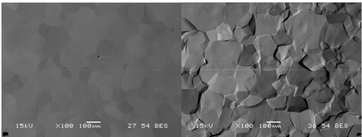
In the Fig. 17 BCP and EP treated niobium samples are compared. It is possible see that the BCP does not smooth out the grain of boundaries as well as EP. More precisely, while after EP the surface average roughness is lower than the initial value, after a BCP process the roughness is higher with respect to the initial value due to the preferential etching at the grain boundaries.
The average roughness Ra of chemically etched niobium surfaces is in the order of Ra =1μm. The step height on etched surfaces at grain boundaries can even be of the order of a few μm. In the electron beam - welded area at the equator, which is also the region of the highest magnetic surface field, the steps can be as high as 30um and are nearly perpendicular to the magnetic field lines.
Fig. 17 Niobium surfaces after BCP etching (left) and EP etching (right)
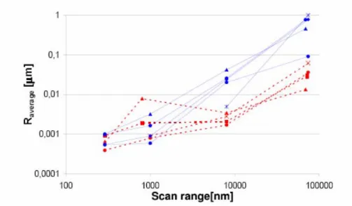
It is well known that surface roughness can lead to geometric field enhancements and therefore to a local breakdown of superconductivity at lower field. The roughness of the EP surface is typically one order of magnitude lower than that of an etched sample on length scales larger than 10 μm as can be seen in the follow Fig. 18:
Fig. 18 Average roughness as a function of the scan length of the atomic force microscope
2.7 Heat treatments
After the large material removal, the cavities are heated to 800 C for 2 hours in a ultrahigh vacuum (UHV) furnace. This step serves two purposes: the removal of dissolved hydrogen from the bulk niobium and the annealing after the deep drawing and welding. In some cases the cavities undergo an additional post purification heat treatment. In this case they are re-heated to 1300 C for four hours. At this temperature all dissolved gases (oxygen, nitrogen and carbon) diffuse out the material. To capture the oxygen coming out of the niobium and to prevent oxidation by the residual gas in the oven (pressure <10-7 Pa), a titanium is placed in the furnace with the cavity. The titanium forms a thin layer on the cavity that is removed by a subsequent 80μm BCP. A low temperature bake that eliminates the Q-drop phenomenon is also used for high gradient cavities. This heat treatment, performed for 48 hours at 120 C, seems to have an effect on the distribution of oxygen just below the Nb2O5 layer.
2.8 High Pressure ultra pure water rinsing
After the heat treatments and chemical polishing steps the cavities are mechanically tuned to adjust the resonance frequency to designed value and to obtain equal field amplitudes in all 9 cells. This process is followed by high pressure water rinsing: in order to remove the residual surface contaminations a jet of ultra clean water with a pressure of around 100 bar is swept over the niobium surface. The mechanical force of the water jet washes particles away very efficiently leaving an almost particle free surface.
After this process, the cavity is dried in a class 10 clean room environment and prepared for final assembly. The assembly stage is very critical since it can be source of additional contamination. [1].
3. QUALIFIES OF MATIERIALS FOR CAVITIES
Introduction
As said, the main component of the ILC, the 33 Km long linear accelerator, is the superconducting RF cavity. Given the actual accelerating gradients achieved with elliptical resonators at 1.3 GHz, a number of roughly ~16000 of these components must be built in order to complete the accelerator.
DESY is historically the laboratory the cavity design was developed and in the past 15 years at least 100 cavities were produced with a large spread of performance.
The present short term plan of the ILC collaboration is to use the manpower and the infrastructure of the main international laboratories such as DESY, KEK, J-Lab, Cornell and Fermilab to produce and condition 100 cavities in the next 3 years with the goal of optimizing and standardizing the process before it is handed out to industry.
In fact the model nowadays considered for the construction of the ILC consists in the division of the production load within the three main regions (Europe, Asia and Americas) with the production and processing carried out in industry.
In order to do so, a number of quality control tools must be developed in the laboratories to check, in a simple and fast way, the consistency of the performance of cavities produced by industry.
The first step toward this direction is the qualification of the Niobium used to fabricate the cavities. At he moment the production rate and consequently the request of high purity niobium is very limited, leading to a small leverage against the big material suppliers which are mostly interested in Nb for other applications which do not require the same specific requirements as SRF cavities. For this reason a number of QC tests have been developed to qualify the consistency of the properties of the material purchased from industrial suppliers.
3.1 Niobium production
The standard technique adopted to produce high purity niobium, as well as for other materials, is electron beam melting. A large cylinder composed of compressed ore is inserted in a furnace and slowly melted and re-melted for several times. During this process the low melting point materials in the ore do evaporate and condensate on the cold areas of the chamber while in the liquid pot the high melting point components float while below the material is cooling and becoming solid. Since the outer rings of the pot do cool down faster, a number of grains with different orientation are generated. The RRR of material melted three to five times is around 800. In order to obtain fine and uniform grains, the ingot is then hot forged at rather low temperature in order to limit the amount of oxidation and maintain the high grade of purity. After forging the material is hot rolled and cold rolled to reach the sheet shape. Between the rolling steps the Nb is annealed in vacuum furnace using titanium getters to reduce the oxygen content and pickled with acid to remove the superficial contaminated layer. At the end of this process the sheets are composed by uniform grains and the RRR is reduced to 300.
3.2 Specifications for fabrications of superconductivity cavities
It is important to distinguish among the properties of niobium, the ones that are related to the cavity’s SRF performances, the formability of the material, and the mechanical behavior of the formed cavity. In general, the properties that dictate each of the above mentioned characteristics have a detrimental effect on one another and in order to preserve the superconducting properties without subduing the mechanical behavior, a balance has to be established. Depending on the applications, some parameters become less important and an understanding of the physical origin of the requirements might help in this optimization. SRF applications require high purity
niobium (high RRR), but pure niobium is very soft from fabrication viewpoint. Moreover conventional fabrication techniques tend to override the effects of any metallurgical process meant to strengthen it. As those treatments dramatically affect the forming of the material they should be avoided. These unfavorable mechanical properties have to be accounted for in the design of the cavities rather than in the material specification.
3.2.1 RRR and purity
The purity of a metal can be characterized by its residual resistivity ratio (RRR), which is defined as the ratio of the electrical resistivity at 295 K to the resistivity at 0 K (ρ295/ρ0). The resistivity at a given temperature (ρT) is proportional to the sum of resistivities from impurities
imp
ρ , crystalline state (grain boundaries density, dislocations…) ρcryst, surface ρsurf , and phonon interaction ρph(T), which is a function of temperature.
( )
T imp cryst surf ph T
ρ ∼ρ +ρ +ρ +ρ 5
If the resistance measurements are performed on sufficiently large, well recrystallized samples, and at very low temperatures, then ρsurf, ρcryst and ρph (T) are negligible, and the residual
resistivity depends mainly on the impurity content of the sample:
Ok i i Ci C ρ ρ ≈ ⎛⎜∂ ⎞⎟ ∂ ⎝ ⎠
∑
6In the case of niobium, the residual resistivity ratio has to be measured at its normal conducting state. For practical reasons it is more convenient to measure the resistance ratio, R295K
/R10K or R295K/R4.2K. At 4.2 K, induction of a magnetic transition from the superconducting state to
the normal state is required. The residual resistance R0 can also be conveniently calculated from
measurements conducted above the critical temperature (Tc = 9.25 K for Nb) and extrapolated to T = 0 K using the simplified law
3 295
o
R = −R αR T 7
Equation is valid for many transition metals, and for niobium α is equal to 5.10 K−7 −3.
The measurement is done using the classical 4-wires method and can be handled in a simple liquid helium Dewar.
The high RRR requirement is related to thermal conductivity rather than superconductivity. BCS theory predicts that the minimum BCS resistance corresponds to a RRR of around 30. Moreover, the surface RRR is expected to be somewhat different from the bulk RRR, and cavities with high as well as low RRR exhibit comparable Q0 at low field. Nevertheless their
behavior at high field is fairly different and can be explained by their thermal properties. Systematic improvement of the quench field is also observed after purification annealing of cavities with Titanium1. Purification annealing is seldom used these days as suppliers can
provide materials with a RRR up to 400. Good thermal conductivity helps to evacuate any thermal dissipation arising from the internal surface toward the external face of the niobium sheet which is in contact with helium, or to cool down parts that are outside the Helium vessel (cut-off tubes or couplers).
Purity and thermal behavior
In the 3 - 15 K range there is a direct relationship between RRR and thermal conductivity. At 4.2 K the thermal conductivity is roughly equal to RRR/4. A superconductor is intrinsically a poor thermal conductor as a part of the (both electrical and thermal) conduction electrons are paired into Cooper pairs and thus cannot contribute to any heat transfer. To improve the thermal conductivity it is essential to get rid of the main scattering sources, i. e. interstitial light elements in the metal matrix. At lower temperature the major conduction mechanism is not related to electron but to phononTi reacts preferentially with Oxygen at temperatures around 800-1000°C. The annealing cycle must include a sufficiently high temperature time in order to evaporate ~ 1 μm of Ti on the surface, and to allow diffusion of Oxygen to the surface. For details regarding the optimization of this process see e.g. In such situations the scattering sources are rather crystalline defects and thus fully recrystallized samples exhibit a large phonon, even with a rather low RRR.
• The phonon peak is a good indication of the crystalline state of the material. When a hot spot occurs, the surface can exhibit temperatures of several K compared to the ~ 2 K of the remaining surface. It is the higher temperature contribution of thermal conductivity that matters.
• With the advent of new cryomodule designs, it is necessary to have parts that were typically made of low RRR material (cut-off tubes, couplers parts), to be made of very high RRR material, when no direct cooling is available. The low temperature conductance is the important parameter in this scenario.
• Another contribution to thermal transfer is the Kapitza resistance, that arises at the niobium-Helium interface. There is a lot of spreading in the possible values for Kapitza resistance of niobium, but as the efficiency of transfer from phonons to “rotons” (~equivalent of phonons inside a fluid) inside helium depends mostly on the effective surface area Seff, rough surfaces are expected to give rise to lower Kapitza resistance.
3.2.2 Mechanical behavior of high purity niobium
The most commonly used mechanical properties are derived from tensile tests (stress-strain curves) and hardness measurements. Tensile tests describe the deformation behavior for an uniaxial case while in most forming processes bi-axial deformation occurs. In addition, specific mechanical tests are available and can be applied to complex forming processes such as hydro forming
In our case, two situations need observation:
- Small deformations: The material exhibits elastic behavior and deformations are reversible. Thus the parameters used to calculate mechanical resistance (stiffness) of finished objects are always linked to the elastic behavior of the material, i.e. Young’s modulus (E), Poisson’s ratio (ν), and to some extent Yield Strength or Elastic Limit (σ0.2). Tensile curves provide an
estimation of the elastic properties of a material, but the values generally include measuring set-up error in the order of 5-10%.
- Plastic deformation. Forming processes necessitate the overcoming of the elastic behavior of the material to obtain formability. The properties that dictate the plastic behavior depend on the material rheology and rupture information, and will be discussed in the next section. Some of the mechanical properties change dramatically with the temperature, and/or thermo mechanical history of the sample material. In particular, annealing (at 800° or higher) of the cavities, works as a "reset" and will erase the effects of cold working from the previous forming steps. Thus, the properties used to calculate the mechanical resistance of a finished cavity must be those of well annealed, fully recrystallized niobium. At a given temperature and purity these parameters have a