CHAPTER 7
Highly conformal growth of microstructured polypyrrole films by
electrosynthesis on micromachined silicon substrates
Abstract
A novel technology for fabricating microstructured polypyrrole (PPy) films is presented based on PPy electrosynthesis on micromachined silicon substrates. PPy light-activated electropolymerization is performed on n-type microstructured silicon featuring lattices of square-like pores with pitch of 8 μm, size (s) of 5 μm, and depth (d) from 5 μm up to 50 μm. Scanning electron microscopy (SEM) highlights as light-activation allows a highly conformal polymer growth yielding a three-dimensional PPy structure perfectly replicating the silicon microstructure to be achieved up to high aspect-ratio (HR=d/s). Arrays of highly ordered PPy hollow microtubes with depth up to 50 μm and thickness up to 1 μm are obtained. Chemical analysis of microstructured PPy films is performed by X-ray photoelectron spectroscopy (XPS) and their electrochemical activity is verified by cyclic voltammetry (CV).
Keywords: Microstructured polypyrrole Highly conformal polymer growth Microtubes
Light-activated electropolymerization Silicon electrochemical micromachining
© 2011 Elsevier Reprinted, with permission, from S. Surdo, L.M. Strambini, C. Malitesta, E. Mazzotta, G. Barillaro, Highly conformal growth of microstructured polypyrrole films by electrosynthesis on micromachined silicon substrates, Electrochemistry Communications doi:10.1016/j.elecom.2011.09.011, with permission from Elsevier – license num 2825870600586
1. Introduction
Conducting polymers (CPs) have been demonstrated to possess interesting properties for applications in different fields, from electronics, chemical sensors to energy storage and surface coatings [1]. Polypyrrole (PPy) is among the most extensively investigated CPs, because of its electrical and optical properties [2] and easy and rapid synthetic schemes. Recently, great efforts have been devoted to the development of technologies for the fabrication of micro/nanostructured PPy-based devices taking advantage of PPy features at the micro/nanoscale, mainly related to larger surface area and three-dimensional (3D) arrangement of polymer chains as compared to bulk material [3,4]. Different morphologies of micro/nanostructured PPy films have been so far obtained [5–8] both by chemical and electrochemical synthesis. The electrochemical preparation ensures a good control of the micro/nanostructured polymer morphology, being it closely related to the experimental conditions (i.e. circulated charge, nature of counter ions, polymerization time). Porous templates (so called “hard templates”) such as alumina [9], silicon (Si) [10], and polycarbonate membranes [11] have been often used for the electrosynthesis of micro/nanostructured PPy films, though the use of “soft templates”, such as soap bubbles [12] and dopant electrolyte [8], has been also proposed. Template-free synthesis of random [7] and ordered [2] PPy nanowires by electropolymerization has been explored as well. The use of hard templates allows a higher control of PPy 3D features to be achieved, being these strictly defined by the template structure. Nevertheless, the reduced flexibility on the morphology of template structures used so far has actually limited feasible polymer morphologies.
A higher degree of flexibility could be achieved by PPy electrosynthesis on microstructured silicon templates whose morphology can be broadly changed and accurately defined by a number of micromachining techniques [13]. To date PPy electrosynthesis has been carried out on flat p- [14] and n-Si [15] electrodes by anodic polymerization, the latter being light-induced to promote oxidation of n-Si via hole generation in the valence band upon photoexcitation [16]. A few works report the electrosynthesis of microstructured PPy on porous silicon templates fabricated from p-Si and highly doped n+-Si [10,17], for which light-activated hole
generation is not required. As we are aware of, no reports on PPy electropolymerization on microstructured n-Si substrates were reported so far. In this work, highly conformal growth of PPy films on micromachined n-Si substrates featuring high aspect-ratio (HR) structures is, for the first time, demonstrated by light-activated electrosynthesis. Arrays of highly ordered PPy hollow microtubes with HR from 1 to 10, depth up to 50 μm and thickness up to 1 μm are fabricated using electrochemically micromachined n-Si substrates as templates. Chemical analysis of microstructured PPy films is performed by X-ray
photoelectron spectroscopy (XPS) and their electroactivity is verified by cyclic voltammetry (CV).
2. Experimental
Microstructured PPy film fabrication is carried out by light-activated electrosynthesis of PPy on microstructured n-Si templates. Microstructured templates featuring lattices of square-like pores with size (s) of 5 μm, pitch (p) of 8 μm, and depth (d) from 5 up to 50 μm (HR=d/s from 1 to 10) are prepared by electrochemical etching (ECE) of n-Si under back-side illumination [18,19]. The starting material is n-Si (die size 2 cm×2 cm), 3÷8 Ω•cm resistivity, (100) oriented, with 100-nm-thick SiO2 layer on top. A lattice of square holes with s=5 μm and
p=8 μm is predefined on the silicon surface by a standard photolithography step followed by buffered hydrofluoric acid (BHF) and hydroxide potassium (KOH) etches. The KOH etch time is tuned to obtain full pyramidal notches to be used as etching seeds during the ECE [18], which is carried out using a solution of HF (48%):H2O (5:37 vol.) additioned with 1000 ppm of sodium lauryl sulfate as
wetting agent. During ECE experiments, the voltage is maintained constant at 3.0 V, while the etching current is linearly decreased with time to etch pores with constant diameter [19]; the etching time is set to 225 and 2100 s to obtain 5 and 50 μm deep pores, respectively. After ECE, samples are rinsed in ethanol and dried by evaporation at 60 °C for 10 min.
PPy films are deposited by galvanostatic polymerization (applied current: 0.2 mA) under back-side illumination of silicon, from a solution of pyrrole 0.1 M in acetonitrile (ACN) containing tetrabutylammonium perchlorate (TBAP) 0.1 M, for different times until a prefixed charge density (50 mC/cm2, unless otherwise specified) has circulated. Illumination is used to enable current flow through the silicon/monomer solution interface, which is otherwise reversebiased for n-Si under anodic polarization. After PPy growth, samples are rinsed in ethanol and dried by evaporation at room temperature.
The experimental setup, used for both silicon microstructuring and PPy growth, consists of a three-electrodes cell with the silicon substrate as working electrode (exposed surface area: 0.78, 1.5, and 12.5 cm2 for flat and micromachined
templates with HR=1 and HR=10, respectively) and two Pt wires as counter and quasireference electrodes, respectively. The cell is provided with a 250W halogen lamp for back-side illumination. The illumination intensity is tuned by changing the lamp power, which is set to a constant value (20% of maximum power) during PPy electrosynthesis and automatically changed to match the etching current setpoint during silicon microstructuring. The samples are electrochemically characterized by CV in TBAP 0.1 M/ACN and analyzed by XPS. Eventually, the
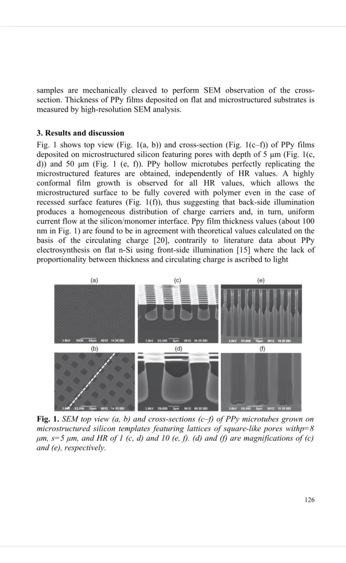
samples are mechanically cleaved to perform SEM observation of the cross-section. Thickness of PPy films deposited on flat and microstructured substrates is measured by high-resolution SEM analysis.
3. Results and discussion
Fig. 1 shows top view (Fig. 1(a, b)) and cross-section (Fig. 1(c–f)) of PPy films deposited on microstructured silicon featuring pores with depth of 5 μm (Fig. 1(c, d)) and 50 μm (Fig. 1 (e, f)). PPy hollow microtubes perfectly replicating the microstructured features are obtained, independently of HR values. A highly conformal film growth is observed for all HR values, which allows the microstructured surface to be fully covered with polymer even in the case of recessed surface features (Fig. 1(f)), thus suggesting that back-side illumination produces a homogeneous distribution of charge carriers and, in turn, uniform current flow at the silicon/monomer interface. Ppy film thickness values (about 100 nm in Fig. 1) are found to be in agreement with theoretical values calculated on the basis of the circulating charge [20], contrarily to literature data about PPy electrosynthesis on flat n-Si using front-side illumination [15] where the lack of proportionality between thickness and circulating charge is ascribed to light
Fig. 1. SEM top view (a, b) and cross-sections (c–f) of PPy microtubes grown on
microstructured silicon templates featuring lattices of square-like pores withp=8 μm, s=5 μm, and HR of 1 (c, d) and 10 (e, f). (d) and (f) are magnifications of (c) and (e), respectively.
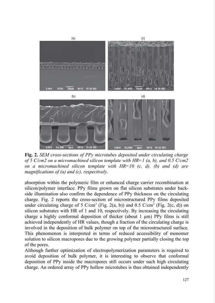
Fig. 2. SEM cross-sections of PPy microtubes deposited under circulating charge
of 5 C/cm2 on a micromachined silicon template with HR=1 (a, b), and 0.5 C/cm2 on a micromachined silicon template with HR=10 (c, d). (b) and (d) are magnifications of (a) and (c), respectively.
absorption within the polymeric film or enhanced charge carrier recombination at silicon/polymer interface. PPy films grown on flat silicon substrates under back-side illumination also confirm the dependence of PPy thickness on the circulating charge. Fig. 2 reports the cross-section of microstructured PPy films deposited under circulating charge of 5 C/cm2 (Fig. 2(a, b)) and 0.5 C/cm2(Fig. 2(c, d)) on
silicon substrates with HR of 1 and 10, respectively. By increasing the circulating charge a highly conformal deposition of thicker (about 1 μm) PPy films is still achieved independently of HR values, though a fraction of the circulating charge is involved in the deposition of bulk polymer on top of the microstructured surface. This phenomenon is interpreted in terms of reduced accessibility of monomer solution to silicon macropores due to the growing polymer partially closing the top of the pores.
Although further optimization of electropolymerization parameters is required to avoid deposition of bulk polymer, it is interesting to observe that conformal deposition of PPy inside the macropores still occurs under such high circulating
of the circulating charge value, conversely to rod-shaped microstructured PPy usually formed on porous silicon substrates [10,17] where a different deposition mechanism is observed based on the complete filling of silicon pores from bottom to top. PPy films deposited on microstructured templates with reduced HR show an outstanding adherence to the silicon substrate independently of film thickness; on the other hand, PPy films on micromachined substrates with high HR seem to have a reduced adherence for larger thickness values that is probably responsible for PPy microtube creasing during the drying step (Fig. 2 (c, d)). The electroactivity and chemical composition of microstructured PPy is investigated by CV and XPS, respectively, as reported in Fig. 3. Fig. 3(a) (top) shows CV curves of PPy films electrosynthesized on flat and microstructured silicon substrates (dashed and solid lines, respectively). Both films show redox peak currents indicating that electroactive PPy is produced by light-activated electrosynthesis on n-Si. The relatively high cathodic currents in the cathodic voltage range, both in direct and inverse scans, are mainly ascribed to the electroactivity of n-Si electrodes under light-excitation conditions. The significant increase of both anodic and cathodic currents on the microstructured PPy, with respect to flat PPy, clearly evidences the larger surface area exposed to electrolytic solution. Fig. 3(a) (bottom) shows the dependence of the anodic peak current ipa for microstructured PPy on the scan rate v. ipa exhibits a linear relationship with v1/2, thus highlighting that the redox process is controlled by charge transport within this thick film. Fig. 3(b) reports detailed XPS spectra of C1s and N1s of
Fig. 3. (a) Top: cyclic voltammograms (1st cycle) of PPy films deposited on flat
(dashed line) and microstructured (HR=1, solid curve) n-type silicon substrates in TBAP 0.1 M/ACN solution. Scan rate: 100 mV/s. Bottom: plot of ipa vs. v1/2 at 1, 5, 10, 25, 50, 75, 100, 150, 200 mV/s. (b) XPS high resolution spectra of C1s (top) and N1s (bottom) of microstructured PPy film electrosynthesized on microstructured silicon with HR=1. Curve fitting components are plotted. Spectra are charging corrected and background subtracted.
microstructured PPy film. Both binding energy and chemical assignment of each component are in good agreement with the literature [21], thus highlighting that the chemical structure of microstructured Ppy film is similar to PPy film deposited on conventional metallic electrodes. The presence of Cl2p signal at 207.5 eV (not shown), assigned to ClO4− species of the electrolyte, reveals that the film is in its
oxidized state. This evidence is further confirmed by the presence of two components at 287.9 eV and 402.8 eV assigned to C=N+ functionality, typical of
non-overoxidized PPy [21]. A certain degree of overoxidation could be properly conferred to the film, thus tailoring its chemical properties to specific applications.
4. Conclusions
The present study describes a novel technology for PPy microstructuring by light-activated electropolymerization of PPy films on micromachined n-Si. SEM analysis demonstrates that highly conformal growth of PPy hollow microtubes with high HR (up to 10) can be achieved on microstructured n-Si by tuning two independent parameters: 1) morphology of the silicon template (i.e. period, side, and depth of the macropore array), which allows tuning PPy microtubes features; 2) electropolymerization conditions (i.e. Circulating charge and time), which allows sizing PPy thickness.
Although the process needs to be still optimized to assure good mechanical stability of PPy microtubes with larger thickness and higher HR, such microstructured PPy films, featuring high surfacearea and thickness ranging from nanometer to micrometer scale, can offer significant advantages for several applications, from chemical sensors to microelectronics and micromechanical devices. Finally, though the highly conformal PPy growth is here demonstrated for specific template morphology, microstructured PPy films with different features can be obtained by properly changing the morphology of micromachined silicon templates.
Reference
_________________________________________________________________ [1] Y. Chen, Y. Luo, Advanced Materials 21 (2009) 2040.
[2] J. Huang, K. Wang, Z. Wei, Journal of Materials Chemistry 20 (2010) 1117. [3] Rajesh, T. Ahuja, D. Kumar, Sensors and Actuators B: Chemical 136 (2009) 275. [4] B. Schulz, I. Orgzall, I. Díez, B. Dietzel, K. Tauer, Colloids and Surfaces A 354 (2010) 368.
[5] A. Kisiel, M. Mazur, S. Kuśnieruk, K. Kijewska, P. Krysiński, A. Michalska, Electrochemistry Communications 12 (2010) 1568.
[6] M. Li, Z. Wei, L. Jiang, Journal of Materials Chemistry 18 (2008) 2276.
[7] M. Woodson, J. Liu, Journal of the American Chemical Society 128 (2006) 3760. [8] M.B. González, S.B. Saidman, Electrochemistry Communications 13 (2011) 513. [9] H. Yan, L. Zhang, J. Shen, Z. Chen, G. Shi, B. Zhang, Nanotechnology 17 (2006) 3446.
[10] K. Fukami, F.A. Harraz, T. Yamauchi, T. Sakka, Y.H. Ogata, Electrochemistry Communications 10 (2008) 56.
[11] S. Demoustier-Champagne, P.-Y. Stavaux, Chemistry of Materials 11 (1999) 829. [12] L. Qu, G. Shi, F. Chen, J. Zhang, Macromolecules 36 (2003) 1063.
[13] M.J. Kohler, Etching in Microsystem Technology, Wiley-VCH, Wheinheim, 1999. [14] J. Yuan, D. Zhang, L. Qu, G. Shi, X. Hong, Polymer International 53 (2004) 2125. [15] R. Noufi, D. Tench, L.F. Warren, Journal of the Electrochemical Society 128 (1981) 2596.
[16] J.M. Bolts, A.B. Bocarsly, M.C. Palazzotto, E.C. Walton, N.S. Lewis, M.S. Wrighton, Journal of the American Chemical Society 101 (1979) 1378.
[17] F.A. Harraz, S.M. El-Sheikh, T. Sakka, Y.H. Ogata, Electrochimica Acta 53 (2008) 6444.
[18] G. Barillaro, A. Nannini, M. Piotto, Sensors and Actuators A: Physical 102 (2002) 195.
[19] G. Barillaro, L.M. Strambini, Electrochemistry Communications 12 (2010) 1314. [20] G. Fortier, E. Brassard, D. Belanger, Biosensors and Bioelectronics 5 (1990) 473. [21] C. Malitesta, I. Losito, L. Sabbatini, P.G. Zambonin, Journal of Electron Spectroscopy and Related Phenomena 76 (1995) 629.