Chapter 7
Single Layer Device Structure: experimental work
7.1Single Layer Device Structure
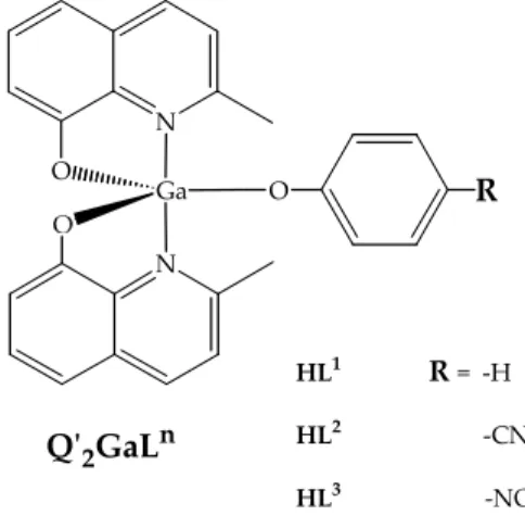
The analysed structural and photophysical properties of the synthesised
Q’2GaLn compounds, reported in Figure 7.1, suggested to verify if they can be
applied as electroluminescent end/or charge transport layer in OLED technologies. N O Ga N O R HL1 R = ‐H HL2 ‐CN HL3 ‐NO2 HQʹ = 2‐methyl‐8‐hydroxyquinoline Qʹ2GaLn
Figure 7.1: Q’2GaLn compounds.
The present study was conducted during four months doctoral stage in the Physic Department of the University of St. Andrews (Scotland, UK) in the laboratory of the Organic Semiconductor Centre, under the supervision of the professor Ifor D. W. Samuel.
7.2 Device preparation
Samples of single layer device where realized using the synthesised
Q’2GaOC6H5 (1), Q’2GaOC6H4CN (2), Q’2GaOC6H4NO2 (3), as
electroluminescent layer. Further GaQ’3 (R) was synthesised in order to
fabricate single layer devices as reference device.
The preparation of all devices samples followed the same protocol.
Indium tin oxide (ITO) conductive coated glass substrate (20 Ω/□ sheet resistance, 4.7 eV work function) was cut by hands in precisely 12 mm2 samples, Figure 7.2. Figure 7.2: ITO coated–glass substrate.
All ITO‐glass samples were cleaned by sonication sequentially three time in ultrasonic bath for 15 min in isopropanol, acetone and chloroform. Each time the ITO‐glasses were dried under strong flux of N2.
On the centre of the cleaned glass samples, was fixed an adhesive tape, 4 mm wide, as a mask to protect the ITO from the wet etching. So to obtain only the ITO strip on the glass as electrode, the rest of ITO was removed by wet etching techniques: Zn powder was gently sprinkled on the samples then HCl was dropped on powder to remove the ITO from the sample surface, then all samples were washed with deionised water.
Again the etched glass samples were cleaned three time by sonication as previously described. Thereafter the samples were exposed to an oxygen plasma in the Plasma Asher chamber (100°C, 10‐2 mbar) for 10 minutes to
remove residual solvents and to enhance the work function of the ITO. The plasma treatment not only reduces the drive voltages considerably, it also suppresses the occurrence of the current anomalies at low voltage.1 So suitable ITO samples, as reported in the Figure 7.3, were obtained. Figure 7.3: etched ITO‐glass samples.
The ITO‐substrates were ready to be coated with coordination gallium compounds films. A 0.019 M dichloromethane (spectrophotometric purity degree) solutions of all compounds were prepared, then its were leaved to stir for two hours in order to be sure to obtain completely solved compounds and homogeneous solutions. The film were fabricated by spin‐coating on the prepared ITO‐glass samples under ambient condition. The spin–coating parameters were: speed: 2500 rpm (round per minutes), ramp: 50 rpm, dwell: 50 sec. These parameters were the same used to collect the photoluminescence quantum yield,
Φ
PL, of the films of all complexes and were selected because of the obtained films show the betterΦ
PL. 7.2.1 Film thicknessAs preliminary work, the thickness of the films prepared with different spin‐ coating parameters were checked by asurface profilometer showed in Figure
7.4.
Figure 7.4: DEKTAK 3 ST profilometer In Figure 7.5 is reported a checked profile example of a GaQ’3 film opportunely scratched. ‐438 30 983 175 ‐2000 0 2000 An gstrom Angstrom GaQʹ3 20 mg,0,5ml, CHCl3 Thickness= 99 nm Figure 7.5: GaQ’3 scratched film profile.
The average value of the checked film thickness deposited from 0.019 M
Zoom
Focus
Spotlight
Sample
Stylus
solutions with the reported spin‐coater parameters ranged from 60 to 70 nm. Better valuation of the film thickness was the ellipsometric data collect on a GaQ’3 film, as reported in the Table 7.1. The film thickness obtained using the
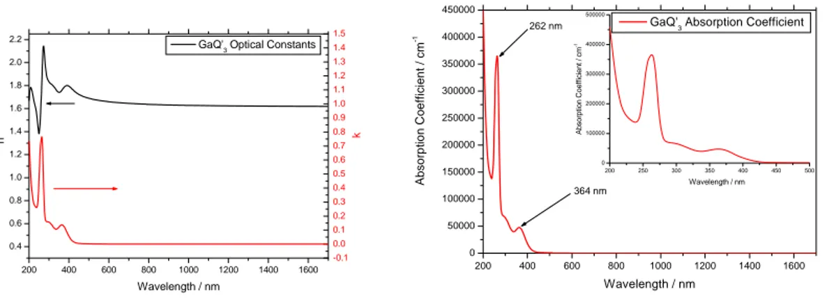
same concentration and spin‐coating parameters was consistent with those checked by profilometer. Sample Thickness (nm)* 1000 rpm 20mg ml‐1 105.4 2500 rpm 20mg ml‐1 75.7 1000 rpm 10mg ml‐1 86.2 2500 rpm 10mg ml‐1 60.0 Table 7.1: spin‐coating parameters, concentration, film thickness. In Figure 7.6, are reported respectively the Ψ and Δ fits, 200 400 600 800 1000 1200 1400 1600 0 2 4 6 8 10 12 14 16 18 20 22 24 26 Ψ / O Wavelength / nm 50O Fit 55O Fit 60O Fit 65O Fit 70O Fit 50O Data 55O Data 60O Data 650O Data 70O Data 200 400 600 800 1000 1200 1400 1600 -100 -50 0 50 100 150 200 250 300 Δ / O Wavelength / nm 50O Fit 55O Fit 60O Fit 65O Fit 70O Fit 50O Data 55O Data 60O Data 650O Data 70O Data Figure 7.6: ellipsometry Ψ and Δ fits. and in Figure 7.7 the optical constant and the absorption coefficient of the GaQ’3 film.
200 400 600 800 1000 1200 1400 1600 0.4 0.6 0.8 1.0 1.2 1.4 1.6 1.8 2.0 2.2 -0.1 0.0 0.1 0.2 0.3 0.4 0.5 0.6 0.7 0.8 0.9 1.0 1.1 1.2 1.3 1.4 1.5 k n Wavelength / nm
GaQ'3 Optical Constants
200 400 600 800 1000 1200 1400 1600 0 50000 100000 150000 200000 250000 300000 350000 400000 450000 200 250 300 350 400 450 500 0 100000 200000 300000 400000 500000 Ab s o rp ti on Coef fi c ien t / c m -1 Wavelength / nm 364 nm 262 nm A b s o rp tio n C o e ff ici en t / c m -1 Wavelength / nm
GaQ'3 Absorption Coefficient
Figure 7.7: Optical constant and Absorption Coefficient of GaQ’3.
7.2.2 Cathode deposition. The absorption coefficient confirm the absorption spectrum of GaQ’3. The coated samples were located on a mask bearing nine positions as reported in the Figure 7.8. All samples ITO side face down, such that ITO stripe runs perpendicular to the slot holes in the mask. Figure 7.8: coated samples on the mask 1 2 3 4 5 6 7 8 9
Immediately the mask was transferred on the holder into the evaporation chamber bearing in alternate way two molybdenum crucibles containing calcium, and two tungsten coils where aluminium is stored.
So once the evaporator achieve the vacuum pressure approximately 10‐7 mbar it
is possible to start with the evaporation of the calcium cathode and the aluminium (4.1 eV) metal capping.
The holder containing the mask rotate to obtain uniform deposition distribution of the evaporated metals. The layer thickness was under controlled variation and the layer sequence could be fabricated in the same vacuum process.
The metal cathode (Ca and Al) were deposited on top of the organic layer without breaking the vacuum. Calcium cathode was covered with aluminium to protect them from degradation under air.
The average deposition parameters for calcium an aluminium are reported in the Table 7.2, aluminium was evaporated two time in order to achieve the desired thickness.
Deposition parameters
Ca Al1 Al2
vacuum ~10‐ 6 mbar ~ 10‐ 6 mbar ~ 10‐ 6 mbar
rate of deposition 0,14 – 0,17 nm /sec 0,10 – 0,12 nm /sec 0,08 – 0,12 nm /sec
current ~ 1,6 A, ~1,2 A ~1,2 A
thickness ~21 nm. ~65 nm ~40 nm Table 7.2: experimental deposition parameter. After the evaporation each of the nine sample of the mask bear four pixel 4 x 1.2 mm2 of surface as described in Figure 7.9.
Figure 7.9: four pixel sample.
The architecture of the single layer device (ITO/ Q’2GaLn (70 nm)/ Ca (20 nm)/
Al (100 nm)) is illustrated in Figure 7.10, is described in Table 7.3.
Figure 7.10: fabricated single layer device structure
ITO and Aluminium ionization potential of and Calcium electron affinity are reported in Table 7.3, 4 mm Al ITO 1.2 mm +
‐
Q’2GaLn Glass ITO Al Ca hνAl Metal Capping Layer, 100 nm Work function = 4.1 eV Ca Catode ‐ provide electrons, 20 nm Work function = 2.9 eV Q’2GaLn Electroluminescent Layer, 60 – 70 nm ITO Anode – provides holes, 20 Ω/ Work function = 4.7 eV Glass Transparent substrate Table 7.3: resumed single layer device characteristics
while the computed electronic state energies of Q’2GaLn are reported in Table
7.4.
Q’2GaOC6H5 Q’2GaOC6H4CN Q’2GaOC6H4NO2
p2 (HOMO) ‐5.20 eV q1 (HOMO) ‐5.70 eV q1 (HOMO) ‐5.73 eV
q2 (LUMO) ‐1.77 eV q2 (LUMO) ‐2.02 eV q2 (LUMO) ‐2.05 eV
Table 7.4: HOMO – LUMO energy levels of Q’2GaLn. 7.3 Device characterization
All devices were fully characterised under ambient and dark conditions without any protective device encapsulation. The light‐current–voltage characteristics were measured with a Keithley 6514 source meter and a Keithley 2400 multimeter measure unit and a calibrated silicon photodiode in front of the light‐emitting pixel at 4 cm of distance. Each of the four pixels was switch on inside a vacuum chamber, to avoid the presence of oxygen and
moisture. The electroluminescence spectra were measured with a Oriel 77400 CCD spectrograph at the temperature of ‐70°C, as illustrated in the Scheme 7.1. The device area was 4.8 x10‐6 m2. All measurement were carried out at room
temperature under vacuum.
Electroluminescence spectra, reported in Figure 7.11, were collected for all device samples except for those obtained with Q’2GaOC6H4NO2 (3) compound.
400 500 600 700 800 900 0,0 0,2 0,4 0,6 0,8 1,0 Qʹ2GaOC6H5 GaQʹ3 Qʹ2GaOC6H4CN Cou n ts (B g co rr ec te d ) Wavelength/nm Figure 7.10: electroluminescence spectra.
As shown in the Table 7.4, The electroluminescence maximum, of the Q’2GaOC6H5 (1) and Q’2GaOC6H4CN (2) device samples, are red shifted about 20
nm respect to the emission on film while the GaQ’3 (R) sample shows a red
shift of 30 nm. The electroluminescence spectra of the Q’2GaOC6H4NO2 (4)
sample is not reported because of the spot light wasn’t enough intense to emerge from the vacuum chamber. Compounds Electroluminescence λ EL/nm GaQ’3 (R) 523 Q’2GaOC6H5 (1) 539 Q’2GaOC6H4CN (2) 526 Q’2GaOC6H4NO2 (3) /
In the Table 7.5 are reported the set up Current – Voltage (I‐V) parameters used during the experiments, on the left, and the photodiode characteristics on the right. Start Voltage 0 Device area 4,8 x10‐6 m2 Stop Voltage 20 V Area photodiode 1 Voltage Steps 200.000 mV Distance 4 cm
Compliance current 0.1 A Resistor 2,2 x 10⁶ MΩ
Steps 100 ms Table 7.5: set‐up I‐V parameters and the photodiode characteristics. ITO Al 1 2 3 4 switchs 1 1 2 2 3 3 4 4 under vacuum, dark conditions CCD camera spectroghraph power source 4 0 0 5 0 0 6 0 0 7 0 0 8 0 0 0 ,0 0 ,2 0 ,4 0 ,6 0 ,8 1 ,0 C ount s (B g co rrec ted ) W a v e l e n g t h ( n m ) Q '2 G a O C 6 H 4 C N Silicon photodiode optical fiber multimeter Scheme 7.1: set‐up for light‐current‐voltage
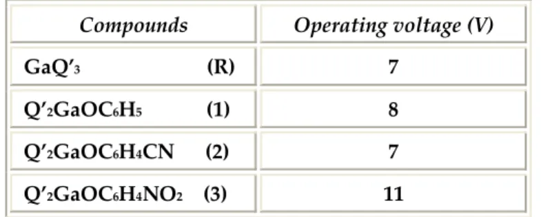
The operating voltages are 7 V for the samples containing Q’2GaOC6H4CN and
GaQ’3 respectively, and 8 V for the device obtained with Q’2GaOC6H5 as
described in Table 7.6. Compounds Operating voltage (V) GaQ’3 (R) 7 Q’2GaOC6H5 (1) 8 Q’2GaOC6H4CN (2) 7 Q’2GaOC6H4NO2 (3) 11 Table 7.6: operating voltage of all samples.
The maximum device operating voltage to avoid the break down is 20 V, this value was observed for all devices. The values reported were confirmed by measurements of different pixels, collected a lot of time in the same conditions. It is possible to observe the low light intensity of sample 3 in the Photodiode Voltage graph reported in Figure 7.11 and the enlarged scale graph in the
Figure 7.12. 0 5 10 15 20 0,00 0,05 0,10 0,15 0,20 0,25 0,30 Q' 2GaOC6H5 Q'2GaOC6H4CN GaQ'3 Q'2GaOC6H4NO2 P h otodi o d e Volt ag e (V) Voltage (V)
0 5 10 15 20 0,00000 0,00002 0,00004 0,00006 0,00008 0,00010 0,00012 0,00014 0,00016 0,00018 0,00020 Q'2GaOC6H5 Q'2GaOC6H4CN GaQ'3 Q'2GaOC6H4NO2 Phot odiode Vo ltag e (V ) Voltage (V) Figure 7.12: Photodiode Voltage – V enlarged scale graphs.
The forward biased Current‐Voltage (I‐V) characteristics of all compounds reported in Figure 7.12, shows current generation in all films, in particular a current enhancement can be observed in the p‐cyanophenol derivative, sample 2, respect to GaQ’3 (R) . 0 5 10 15 20 0,000 0,002 0,004 0,006 0,008 0,010 0,012 0,014 0,016 0,018 0,020 0,022 0,024 Qʹ2GaOC6H5 Qʹ2GaOC6H4CN GaQʹ3 Qʹ2GaOC6H4NO2 Cur re n t (A) Voltage (V) Figure 7.12: Current‐Voltage (I‐V) characteristics The behaviour of device 2 is reflected in the Current Density (J‐V) graph, Figure
7.13, were the current quantity, generated into the device, enhance quickly respect to the sample R at 15 V. 0 5 10 15 20 0 100 200 300 400 500 Qʹ2GaOC6H5 Qʹ2GaOC6H4CN GaQʹ3 Current De ns ity (m A/ cm 2 ) Voltage (V) Figure 7.13: Current Density (J‐V) graph.
The Luminance – Voltage (L‐V) graph (Figure 7.14) describe the brightness quality of the obtained pixels. So as it can be observed the device obtained with the p‐cyanophenol derivative shows the better luminance both at low and high voltages. The Luminance value at 20V are reported in the Table 7.7 while the enlarged Luminance scale is reported in Figure 7.15, to appreciate the different behaviour at lower voltages. The Luminance values at 15V are reported in
0 5 10 15 20 0 100 200 300 400 500 Q' 2GaOC6H5 Q'2GaOC6H4CN GaQ'3 Lu mi n anc e (Cd /m 2 ) Voltage (V) Figure 7.14: Luminance – Voltage (L‐V) graphs. Compounds Luminance Cd/m2 (20V) Current Density mA/cm2 (20V) GaQ’3 (R) 43 234 Q’2GaOC6H5 (1) 2.7 234 Q’2GaOC6H4CN (2) 465 464 Q’2GaOC6H4NO2 (3) / / Table 7.7: Luminance and Current Density values at 20 V. 0 5 10 15 20 0 10 20 30 40 50 Q'2GaOC6H5 Q'2GaOC6H4CN GaQ'3 Lu mi na n ce (C d/ m 2 ) Voltage (V) Figure 7.15: enlarged Luminance scale.
Compounds Luminance Cd/m2 (15V) GaQ’3 (R) 7 Q’2GaOC6H5 (1) 0.3 Q’2GaOC6H4CN (2) 35 Q’2GaOC6H4NO2 (3) / Table 7.8: Luminance values at 15V. The same behaviour is checked in the Power Efficiency graphs. Device 2 shows better power efficiencies values at low voltages, the maximum is found at 14 V. The maximum Power Efficiency is shifted and at 15 V for device 1, while for
GaQ’3, device R, the maximum enhance towards 16 V. So the better efficiencies,
respect to the current and power (Figure 7.16) consumption, are those of
Q’2GaOC6H4CN, sample 2, at lower operating voltage than GaQ’3, sample R,
ranging from the 7 V to 15 V. The power efficiencies at 15 V are reported in
Table 7.9. 0 5 10 15 20 0,000 0,002 0,004 Q'2GaOC6H5 Q'2GaOC6H4CN GaQ'3 Po w er E fficiency (l m/W ) Voltage (V) 0 5 10 15 20 0,00 0,01 0,02 0,03 Q'2GaOC6H5 Q'2GaOC6H4CN GaQ'3 Pow er Ef ficiency (Cd /A ) Voltage (V) Figure 7.16: on the left Power Efficiency (lm/W); on the right Power Efficiency (Cd/A).
Compounds Power Efficiency lm/W (15 V) Power Efficiency Cd/A (15 V) Q’3Ga (R) 4 10‐3 1.9 10‐2 Q’2GaOC6H5 (1) 3.4 10‐4 1.8 10‐3 Q’2GaOC6H4CN (2) 4 10‐3 1.8 10‐2 Q’2GaOC6H4NO2 (3) / / Table 7.9: Power Efficiency at 15 V. The External Quantum Efficiency percentage (EQE%) was calculated following the metod studied by Greenam et al. 2
The behaviour of Q’2GaOC6H4CN device, sample 2, previously described is
retained in the calculation of the EQE%. In graphs, reported in Figure 7.17, sample 2 shows the better EQE% at lower voltages, between 7 V to 15 V, respect to the other devices. 0 5 10 15 20 0,00 0,02 0,04 0,06 0,08 0,10 Q'2GaOC6H5 Q'2GaOC6H4CN GaQ'3 EQE% Voltage (V) Figure 7.17: External Quantum Efficiency (EQE%) graphs. The maximum values of EQE% of all device are reported in the Table 7.10.
Compounds External Quantum Efficiency % GaQ’3 (R) 0.1 % (17 V) Q’2GaOC6H5 (1) 0.044% (15 V) Q’2GaOC6H4CN (2) 0.07% (14 V) Q’2GaOC6H4NO2 (3) / Table 7.10: External Quantum Efficiencies %. The collected measurement allow the possibility to calculate the CIE coordinate, Table 7.11. As reported on the CIE diagram of the Figure 7.19, it is possible to evaluate the colour quality of each obtained pixels. Compounds CIE coordinates (x, y) GaQ’3 (R) x = 0.363, y = 0.511 Q’2GaOC6H5 (1) x = 0.341, y = 0.486 Q’2GaOC6H4CN (2) x = 0.307, y = 0.497 Q’2GaOC6H4NO2 (3) / Table 7.11: CIE coordinates. The better colour performance related to the PAL colour system, is showed by the device obtained with Q’2GaOC6H4CN as electroluminescent layer. The
comparison of the colours position are reported in the Figure 7.20.
Figure 7.20: CIE (x,y) chromaticity diagram. 7.4 Conclusions Single layer devices were favricated with the architecture illustrated in Figure
7.21. All Q’2GaLn compounds were tested as electroluminescent and/or a charge
transport layer. The devices sample performances were compare with a reference built with GaQ’3, synthesised for these experiments.
ITO/ Q’2GaLn (70 nm)/ Ca (20 nm)/ Al (100 nm) GaQ’3 device: x = 0.363, y = 0.511 Q’2GaOC6H4CN device: x= 0.307, y= 0.497 Q’2GaOC6H5 device: x= 0.341, y= 0.486 Q’2GaLn Glass ITO Al Ca hν
The better performance were observed for the devices sample containing
Q’2GaOC6H4CN as electroluminescent layer. The collected data confirm better
EQE%, Luminance and Power Efficiencies than those registered for the device with Q’2GaOC6H5 as electroluminescent material. The sample containing
Q’2GaOC6H4NO2 as electroluminescent layer show a very weak
electroluminescent emission confirming the trend observed in the photophysical characterization. The behaviour Q’2GaOC6H4CN sample is
probably due to a more efficient charge transport mechanism involving the hole conduction. The measurements are in agreement with the supposed charge transport properties derived from the structural data analysis, the photoluminescent properties and the computation of the electronic states.
REFERENCES
1. Berleb, S.; Brütting, W.; Schwoerer, M. Synth. Met. 1999, 102, 1034.
2. Greenham, N. C.; Friend, R. H.; Bradley, D. D. C. Adv. Mater. 1994, 6, 491.