1 Introduction
The major challenge the semiconductor industry is confronted with for the last few years has been to design “system-on-chips” (or SoCs) with far more complex functionality and domain diversity than in the past, yet in significantly less time.
At the very top of the list of challenges to be solved is verification.
General agreement among many observers is that verification consumes at least 70 percent of the design effort.
Design reuse by means of semiconductor intellectual property (IP) is becoming the centre of gravity for design productivity and the key to being able to produce chips that really work.
Clearly, methodology and tools are critical in bringing IP to play in the SoC design environment. Verifying final design correctness is viewed as the key barrier to designing ever more complex SOCs and exploiting leading-edge process technologies.
An additional observation is that no single design tool could be used to solve the problem but, a complex sequence of tools and techniques are needed to reduce the number of design errors to an acceptable minimum.
Every reusable design block needs to be accompanied by a reusable “complete” testbench or verification suite for thorough intra-block verification.
1.1 Design Driven by Differentiation, Cost and Time to Market
In many ways, technology and the economic environment are inseparable. The semiconductor industry is driving growth in many new markets. Consumer demand for electronics in those new markets, in turn, dictates the health of the global semiconductor ecosystem.
In order to be successful in these markets, designers must focus on three elements: differentiation, cost and time to market.
The primary concern for designers has to be differentiation.
Differentiation in chip design can occur in a variety of areas: functionality, performance, power consumption, form factor and even price. Without differentiation, new chips have no chance in the market.
Cost is a factor that has grown dramatically in importance over the past few years. Cost is multi-dimensional and depends on the parameters of the design, the impact of manufacturing and the support required. Cost is also affected by factors within the business environment; most recently, the economic downturn and the push toward globalization. Both employment and market growth in new global regions will have an increasing impact on design cost.
In conjunction with the explosion in design complexity, fast reductions in the time-to-market (TTM) demands for electronic devices are occurring.
Not only are the TTM design cycles shrinking for all application spaces, but this is accompanied by a migration away from traditional applications (military and Industrial) to consumer products, which have the shortest cycle times. This shift is causing the average cycle time to be shrinking at a faster rate than any one market segment. Worldwide growth of mainstream consumer applications such as DVD players, game consoles and cellular handsets has raised the stakes for timely delivery of high-volume, price-sensitive consumer ICs. In the past, semiconductor manufacturers could tolerate delays in development and still recover significant profit while products lingered for years in the marketplace. Today, product cycles have shrunk to mere months and any delay in IC delivery means correspondingly less time to recover costs and accumulate profit.
Clearly, these verification activities have to be performed more efficiently if the overall market challenges are to be met.
1.2 Technology Pressure
Within the context of this economic pressure, we also have a set of dramatic changes to the technology. The industry has progressed to finer geometry processes on a schedule that has, so far, run almost like clockwork.
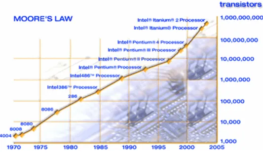
We saw the move from 0.65-micron to 0.5, then 0.35 and 0.25, to 0.18. Now the geometry of choice for new designs, has reached 90 nm in production, 65-nm process technology is in development phase, research is approaching 45-nm, 32-nm and 22-nm process technologies [1]. Figure 1-1 shows how the current silicon chip technology is evolving.
Figure 1-1: Moore’s law
Moore, one of the founders of Intel, observed in an article in the April 19, 1965 issue of Electronics magazine [2] that innovations in technology would allow a doubling of the number of transistors in a given space every year (in an update article in 1975, Moore adjusted the rate to every two years to account for the growing complexity of chips), and that the speed of those transistors would increase. Each time transistor size shrinks, integrated circuits (ICs) become cheaper and perform better. Due to the increasing
complexity the design of these systems is getting much more difficult and it drives a major set of challenges in the verification process. One manifestation of this pressure is the number of advanced chip design re-spins that are due to the discovery of functional errors. Research by Collett International Research [3] [4] suggests that:
• 61 percent of all chip designs require at least one re-spin.
• Of these, 71 percent have functional or logic bugs.
1.3 Design Productivity Gap
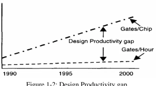
Design productivity lags the design density improvements made possible by the technological evolution.
Figure 1-2 shows this design productivity gap. The gate density is shown in Gates/chip and the design productivity is shown in Gates/hour.
Figure 1-2: Design Productivity gap
The increasing complexity of ICs poses challenges to both system design engineers and verification engineers.
This productivity gap cannot be addressed by simply throwing more engineers at the problem. For one thing, there are not enough qualified engineers to solve the problem and, even if there were, there are practical limitations on how large a design team can grow. As design teams grow, so does the level of coordination required to keep everyone in sync.
Instead, new methodologies that make the design process more productive are required. The industry has responded to this challenge by adopting design reuse strategies.
By utilizing pre-existing blocks (also know as intellectual property (IP) blocks or virtual components (VC)), the amount of original design work required to realize a new design is reduced.
With platform-based design, design reuse goes beyond reusing individual blocks. In platform-based design, a set of core elements that are common across a family of products is identified, integrated, and verified as a single entity. The actual products are then realized by adding individual design elements to this core. This approach will be shown in this thesis work.
The individual elements can be either additional IP blocks or newly authored elements.
1.4 Aim of this work
The development and integration of intellectual property in the form of large functional blocks or cores is an essential part of an increasing number of today's IC design strategies. Numerous benefits justify this approach. Properly managed, the use of pre-designed, pre-verified IP blocks can cut man-months off of the design cycle, provide opportunities for design reuse in future systems, and where applicable, ensure compliance with complex standards and protocols. Unfortunately, the emergence of the IP-based design methodology has done as much to exacerbate design and verification problems associated with systems-on-chip (SOC) designs as it has to alleviate them.
Designs in every industry segment as automotive and aerospace for example are built around interfaces such as PCI, USB or I2C. Unfortunately for design and verification teams, these standards are all described in documents, many in the 500+ page range, all containing the unavoidable ambiguities subject to human interpretation.
In the case of PCI Express, USB or I2C, the standard allows for an extremely wide range of device types, features, and functionality, and few chip designs are implementing 100% of the features defined in the specification. Verifying these interfaces is becoming an increasingly significant challenge for chip designers.
The two key elements to interface verification are verifying compliance with the specification, and verifying interoperability with other compliant devices.
Compliance verification is largely defined as ensuring that a design adheres to the features and functionality defined in the specification from the standards bodies.
The ultimate goal is to ensure that designs can interoperate, or communicate, with other devices in the end system using the interface standard. However, with the freedom to implement various subsets of the functionality defined by a particular protocol specification comes the added risk of incompatibility between compliant devices.
Compliance does not necessarily guarantee interoperability.
Commercial verification IP solutions provide the ability to completely verify the interface for compliance and interoperability. Obviously, all elements of the verification IP must be easily integrated into an existing verification environment and methodology. Interface verification solutions have an additional requirement of being highly portable to support easy deployment into all commercial verification tools and languages.
Aim of this work is the development of a complete verification and validation flow for a new software programmable I2C/SPI interface on APB BUS.
The work has been organized as follows:
a. Timing and Functional verification of the I2
C/SPI stand alone b. Design of an embedded system featuring the I2
C/SPI on AMBA Bus
c. Development of the drivers for the peripheral and FPGA prototyping of the system The SPI module of our interface has been developed by the company Sensor Dynamics [5] and it was validate from their engineer. The details of the implementation of that module are covered from industrial secret. The thesis work has been then focused on
the new I2C module. The SPI and I2C modules share both the interface registers on the APB AMBA BUS and the output pins. Which module has to be used is software programmable.
1.5 The choice of the Processor
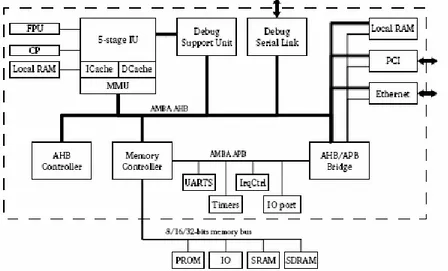
Due to the collaboration with the company Sensor Dynamics [5] that performs research and development activities based on the LEON-2 [6] platform, our embedded system has been designed using this processor.
LEON-2 is a synthesizable processor developed by ESA and maintained by Gaisler Research [7] and it targets both the ASIC and FPGA markets.
It’s a 32-bit RISC SPARC V8 compliant architecture, and uses big endian byte ordering as specified in the SPARC V8 reference manual [8]. More details are given in chapter 3.
An overview of the LEON-2 processor architecture can be seen in the Figure 1-3
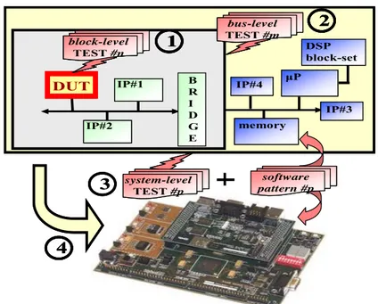
1.6 Verification methodology and approach
The validation of the I2C/SPI Interface has been performed at different verification levels: starting with the lowest one (single IP) and terminating with the highest one (system) [9] [10]; particularly the verification process is composed by four steps in ascending hierarchy order: block-level, bus-level, system-level simulations and hardware emulation. μP DSP block-set memory IP#3 IP#4 μPμP DSP block-set DSP block-set memory memory IP#3 IP#3 IP#4 IP#4 4 4 4 IP#2 IP#1 B R I D G E IP#2 IP#2 IP#1 IP#1 B R I D G E system-level TEST #p system-level TEST #p software pattern #p software pattern #p 3 3 DUT DUT block-level TEST #n 1 block-level TEST #n block-level TEST #n 11 bus-level TEST #m 2 bus-level TEST #m bus-level TEST #m 2 2
Figure 1-4: Verification methodology
The block- and bus-level simulation (Figure 1-4 – step 1 and step 2) aims to verify the IP functionality when it is considered as stand alone. The checks are related to the reset condition (signals and register values), to the register read/write accesses and to the IP behavior while performing its functionality. The IP-level simulation usually requires a master agent (for register accesses) a slave model (to be accessed by the DUT) monitors and for bus peripherals a bus functional model (BFM). The VSI (Virtual Socket Interface) Alliance [11] recommends this to get a notably degree of re-usability to the DUT and to
allow easy IP check-in when it has to be integrated into different SoC projects. At this level a self-checking testbench using VHDL language has been written.
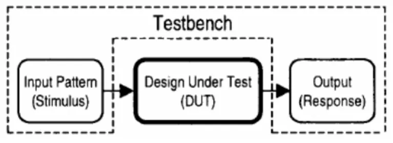
A testbench is a layer of code that is created to apply input patterns (stimulus) to the design under test (DUT) and to determine whether the DUT produces the outputs expected. Figure 1-5 shows a simple block diagram of a testbench that surrounds the DUT.
Figure 1-5: Testbench block diagram
A testbench that is created to apply inputs, sample the outputs of the DUT, and compare the outputs with the expected (golden) results is called a self-checking testbench, as shown in Figure 1-6. A self-checking testbench generates errors if the sampled outputs do not match the expected results. It also indicates the status of the inputs, outputs obtained, and expected results along with error information. This helps in analyzing the DUT’s detail functionality and isolating the cause of the error. Figure 1-6 shows a block diagram of a self-checking testbench that surrounds the DUT.
Figure 1-6: Self-checking Testbench block diagram
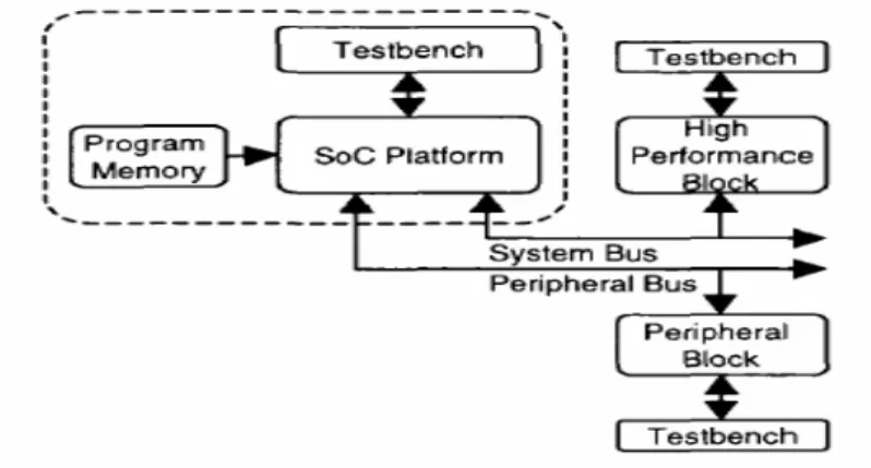
previous phases is that in this environment the processor, the Leon core in our case is used to perform all operations needed to verify the IP. This means that software patterns need to be written; the most suitable language is Assembly, for the close correspondence between the actions to be done and what is really performed by the processor. The checks are related to the reset condition (register values), to the register read/write accesses and to the IP functionality. Since this simulation involves the system as a whole, all possible interactions between the DUT and the other IPs have to be tested. The use of software to performs the various checks does not prevent the self-checking characteristic to be exploited: the expected results are written along the Assembly code rather than in VHDL; finally the mechanism to alert the user in case of failure is slightly different, consisting on use of some I/O signals as flag to indicate the status of the test (running, finished, successful or failed). Figure 1-7 shows a typical block diagram of a system verification environment:
Figure 1-7: Soc block diagram
In the hardware emulation phase (Figure 1-4 – step 4), the system is being mapped onto the prototyping board and all software patterns written for the system-level simulations are compiled and loaded in the board memory; each test becomes a program that runs on the board and produces a positive result in case the test passes, or negative result otherwise.
This phase allows useful timing verification, since the IP can be verified at system level in the real hardware environment. Additional system-level verification is performed during this phase, since it is possible to execute the desired application under practical
working conditions, further increasing the level of reliability. The board used in this work is a VIRTEX II based development board from Memec design. See chapter 6 for more details.
1.7 Thesis outlines
• Chapter 1: An introduction to “system-on-chips” (or SoCs), to the verification challenge and the aim of this thesis work are presented.
• Chapter 2: A background review on the I2
C and SPI protocol and on the AMBA Bus is given. Then the main characteristics of the new Interface I2C/SPI on APB Bus are presented with the description of the registers and of their functionality.
• Chapter 3: An overview of the main characteristics of the LEON processor and some details useful in the development of this work are given
• Chapter 4: The Validation and Verification process of the Interface is presented. The steps performed to prove the compliance to the protocol and the interoperability are described. Some case examples are given.
• Chapter 5: The firmware development work is presented in this chapter giving first an overview on the SPARC V8 ISA.
• Chapter 6: The prototyping process on the Memec development board of the Leon featuring the I2C/SPI interface is presented. Some case examples are given.
• Chapter 7: Presents the conclusions of this work