4 Quasi-Asynchronous optical
sampler experimental results
4.1 Frequency difference locking issue
In this thesis an optical sampler which exploits a mixed technique is proposed. This kind of sampler is called Quasi-Asynchronous (Fig. 4.1).
Fig 4.1: Generic set up of the proposed Quasi-Asynchronous sampler.
In Figure 4.1 is shown a generic setup of the sampler which has been implemented in the laboratory of CNIT-CEIIC in Pisa. The "frequency difference locking" block consists in a double PLL (Phase-Looked Loop) which has to keep constant the frequency difference between the signal under test and the sampling signal. Later we will see how this imposed frequency difference will trigger the oscilloscope to
correctly visualize the signal measured by the optical sampler, avoiding any post processing for samples re-ordering.
First of all it is necessary to understand how a classic PLL works: a phase-locked loop is an electronic control system that generates a signal that is locked to the phase of an input or "reference" signal. A phase-locked loop circuit responds to both the frequency and the phase of the input signal, automatically raising or lowering the frequency of a controlled oscillator until it is matched to the reference in both frequency and phase. A phase-locked loop is an example of a control system using a feedback.
Fig. 4.2: scheme of a classic PLL
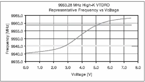
The VCO (Voltage Controlled Oscillator) is an essential stage of the PLL [15]; it is an oscillator whose output frequency depends on the applied input voltage. Generally this dependence is not linear, as shown in Figure 4.3.
Fig. 4.3: Characteristic of the VCO used in our experiments. Changing the input voltage the output frequency
A fundamental property of the PLL is the fact that at the steady state, if the input is a constant frequency, the output tends to a frequency which is perfectly the same as the input. The input signal v(t) [16] can be written as:
( )
cos 2 v( )
v t =A ⎡⎣ π f t+ϑ t ⎤⎦ (4.1)
with θ(t) phase to be estimated referred to the frequency fv. The v(t) instantaneous
phase is compared (through the mixer which works as a phase detector) with the instantaneous phase of the signal:
( )
2sin 2 ˆ( )
v v
v t − ⎡⎣ πf t+ϑ t ⎤⎦ (4.2)
which is produced by the VCO, whose output is a signal with a instantaneous frequency which is the sum of fv and of a quantity proportional to the check voltage
vc(t):
( )
( )
ˆ v c d t k v t dtϑ = (4.3)where kv [rad/(V·sec)] is the VCO constant.
The phase detector output is the error signal e(t) which depends on the phase error:
( )
t( ) ( )
t ˆϕ ϑ −ϑ t (4.4)
Using the tunable gain and the VCO input voltage offset it is possible to bring the VCO to cancel the phase error φ(t). When the phase error is canceled the signal v(t) is locked in phase (and obviously in frequency as well) with the signal vv(t) and this is the
reason why the name of this electronic component is Phase-Locked Loop. Differentiating the (4.4) it is possible to obtain the PLL equation:
( )
( )
v( )
( )
d d
t t k e t
where γ(t) (loop filter) takes account of the effects of the tunable gain and the output bandwidth of the mixer.
In the laboratory a classic PLL, as the one shown in Figure 4.2, was implemented. In our experiments both the signal under test and the sampling signal will have reference clocks at about 10 GHz. For that reason we exploited a mixer (Miteq DB0218LW2) with input and output bandwidths of 2÷18 GHz and DC÷750 MHz respectively. In our case the electrical reference clock coming out from the PicoSource represented the input frequency fv (~10 GHz).
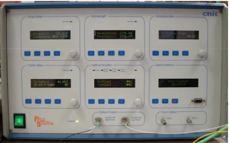
In particular, the PicoSource (Fig. 4.4) is an optical pulsed source based on an actively mode-locked fiber loop, implemented and realized in CNIT-CEIIC laboratories in Pisa. It can generate a 10GHz pulse train with a pulsewidth of ~3.5ps.
Fig. 4.4: PicoSource front panel. There is the possibility to set the optical carrier wavelength. To lock the cavity
modes phases it is possible to tune the optical cavity delay, to shift the phase or to set the Mach-Zender modulator bias voltage.
Mode Locking (ML) represents one of the most suitable techniques [16] to obtain transform limited and ultra-short optical pulses (i.e. the produced pulsed signal exhibits the minimum bandwidth-time product). This is a technique for generating periodic optical pulses from a multimode laser oscillator, forcing the mode-relative phases. In particular, ML refers to the situation where the cavity modes are made to oscillate with
This technique is used in semiconductor and fiber lasers with different methods to lock the phase of the optical modes. For both these technologies, three possible realizations exist, depending on the device forcing the phase: active mode locking (AML), where a phase or amplitude modulator is inserted into the laser cavity, passive mode locking (PML), where an optical passive device, as a saturable absorber, is inserted into the cavity to force the phaselocking condition, and hybrid-mode locking (HML) if a control signal or an externally controlled passive device is used to help the ML operation.
The fiber AML laser represents a good choice for OTDM applications because of its high output power, its sech2 transform limited shape (Fig. 4.5) without a pedestal, and its tunability over the whole optical bandwidth of the optical amplifier.
optical spectrum
Fig. 4.5: Spectrum of the ultra-short optical pulses generated by the PicoSource.
In the next pictures it is possible to see how the frequency generated by a 10 GHz VCO (Fig. 4.3) is locked (or not) to the PLL input frequency. In particular, in Figure 4.6 the oscilloscope was triggered by the PicoSource reference clock, the blue trace is the PicoSource photo-detected output and the green one is the VCO output (locked). In Figure 4.7 it is possible to see what happens when the VCO output is not locked to the Picosource frequency.
Fig. 4.6: Pico Source electric signal (blue) locked to the VCO output (green).
Fig. 4.7: Example of non-locked signals in the PLL.
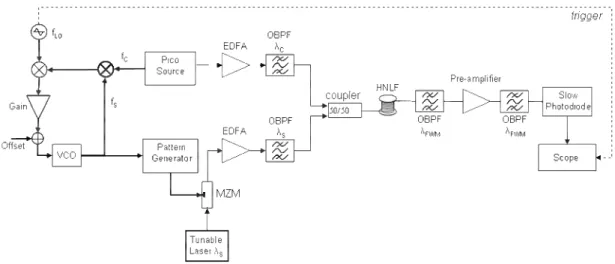
Now it is possible to introduce the nonstandard PLL used to synchronize the quasi-asynchronous sampler. The difference between the two PLL consists in the fact that in the nonstandard one there are two different mixers to impose and maintain a fixed frequency mismatch between the sampling signal and the signal under test (Fig. 4.8).
The first mixer function consists in detecting the frequency difference between input signal and sampling signal; the second one (a low frequency mixer, with input bandwidth of 0.1÷125MHz and output bandwidth of DC÷75MHz) is the mixer of an equivalent classic PLL scheme where the local oscillator (fLO) represents the input
signal. In this case we lock the frequency |fc-fs| to a value fLO.
In the next two pictures the output of the first mixer (|fc-fs|) is shown. In Figure
4.9 the frequency mismatch is fixed to 1MHz, whereas in Figure 4.10 the difference between the two frequencies reached the value of 100KHz. In both the cases, the oscilloscope has been triggered by the local oscillator reference clock, shown in Figure 4.9 and 4.10 as a square wave in the top of the picture.
Fig. 4.9: Frequency mismatch fixed to 1MHz (bottom) and local oscillator reference clock (top).
Fig. 4.10: Frequency mismatch fixed to 100KHz.
The frequency mismatch leads to a shift of the sampling signal on the signal under test in time domain. As shown in Figure 4.11, exploiting this imposed frequency shift of
the sampling pulse train on the periodic signal under test, it is possible to obtain and correctly visualize the sampled signal envelope.
Fig. 4.11: Quasi-Asynchronous sampler working principle.
As it is explained in Chapter 3 (3.5), we impose that
2
= ∆ ⋅
LO s
f T f (4.6)
obtaining in our case a ∆T of 1fs (fLO=105, fs=1010). In this way samples are
consecutively collected, so no post processing is required (Fig. 4.12) and through the electrical nonstandard PLL scheme, the difference between the signal frequency and the sampling frequency is maintained constant.
4.2 Sampling of a sinusoidal signal exploiting FWM
In this first setup a continuous wavelength (CW) λs modulated by a pattern
generator clock signal through a Mach-Zender modulator, has been used as signal under test which is sampled by means of ultra-short pulses generated by the PicoSource (Fig. 4.12).
Fig. 4.12: Setup used in the first experiment.
The signal under test is considered to be periodic with a frequency fs=1/Ts. On the
other hand, the sampling signal is an ultra-short pulse train with a frequency fc=1/Tc,
where the mismatch between the two frequencies is fixed and maintained constant by the nonstandard PLL.
The wavelengths used in this setup are: λs=1553.48 nm, λc=1550.44 nm and
λFWM=1547.38 nm (partly degenerate FWM, that is λFWM=2λc-λs). The signals
frequencies are: fc=10GHz and fLO=500KHz, while fs is imposed by the PLL, so fs=fc
-fLO=9.999995 GHz.
Both the sampling signal and the signal under test are amplified by EDFAs (Erbium Doped Fiber Amplifier) and then filtered to limit the ASE noise introduced by the amplifiers. Then they are coupled and launched into 500mt of HNLF (High NonLinear Fiber).
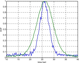
10 15 20 25 30 35 40 0 0.1 0.2 0.3 0.4 0.5 0.6 0.7 0.8 0.9 1 time [ps] AC F
Fig. 4.13: Comparison of the sampling pulses autocorrelation before the EDFA (blue line) and after the OBPF (green
line).
The sampling pulsewidth has been monitored by an autocorrelator (Fig. 4.13): its autocorrelation is about 4.5ps before the EDFA and 8ps after the OBPF (before the coupler). This enlargement is due to the fact that the OBPF (introduced to limit the EDFA ASE noise) has a bandwith about 2nm which cut the original larger sampling pulse bandwidth (Fig. 4.6).
1542 1544 1546 1548 1550 1552 1554 1556 1558 1560 1562 -70 -60 -50 -40 -30 -20 -10 wavelength [nm] signal sampling pulse FWM term
We induce FWM between the two optical signals into the HNLF (Fig. 4.14): every pulse of the sampling signal generates a pulsed FWM component, whose power is proportional to the signal under test instantaneous power in the corresponding interaction time (and to the square power of the sampling pulse).
Fig 4.15: FWM terms proportionality.
Signals wavelengths (therefore their spacing) are chosen in order to obtain an efficient FWM term (see Chapter 2, equation (2.18)) as shown in Figure 4.14.
An optical tunable filter is then used to select the FWM component whose wavelength is closer to λc, so that the energy of the obtained samples is linearly
dependent on the instantaneous power of the signal under test (Fig. 4.15). The optical samples are then amplified through the pre-amplifier and filtered again to reduce the noise introduced by the amplifier.
Now it is possible to reconstruct the sampled signal using a slow photodiode (bandwidth of 125MHz) and a low-bandwidth oscilloscope (Fig. 4.17) to obtain just the envelop of the samples train. As shown in Figure 4.12, the oscilloscope is triggered with
fLO, even if the samples frequency at the receiver is still fC, but as explained in Chapter
3, using the slow photodiode it is possible to correctly reconstruct the envelop of the samples train, and the acquired signal itself has a new period equal to 1/fLO.
Fig. 4.16: Sampling pulses visualized with a 10GHz photodiode.
Fig. 4.17: Signal under test (blue) visualized with a 10GHz photodiode and acquired signal (red).
Looking at Figure 4.17 it is possible to understand that the signal to be sampled is periodic at 10GHz but it has also a relevant component at 20GHz. It is also easy to see that the noisiness on the high level manifests itself yet in the original signal, so it is not to impute to the sampler process. In the next picture the signal under test and the acquired signal are overlapped, after a time axis rescaling. The acquired signal slight distortion is probably due to the excessive width of the sampling pulses (more than 5 ps).
0 0,2 0,4 0,6 0,8 1 1,2 0 20 40 60 80 100 120 tim e [ps] n o rm al iz ed am p lit u d e
Fig. 4.18: Signal under test (violet) and acquired signal (blue).
4.3 Sampling of Return-to-Zero signals exploiting
XPM-based polarization rotation
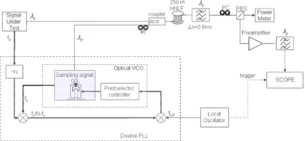
The generic setup of this second experiment is shown in Figure 4.19.
Let’s focus our attention on the double PLL scheme, which imposes the frequency mismatch between the repetition rates of the two signals. In this case it is necessary to explain that if the signal under test is periodic with T=NTb (being Tb the bit time and N
the sequence bit number), the period of the sampling signal can be chosen as
Tc=NTb+∆T, where ∆T (500fs in this case) is the desired temporal resolution. Through
the electrical PLL scheme, the difference between the N-th sub-multiple of the signal
bite rate f s =1/Tb and the sampling frequency (fLO=fs/N-fc) is maintained constant.
In this scheme (Fig. 4.19) the Mode-Locking (ML) Source is used as a sort of VCO into an equivalent VCO (Optical VCO) of an electric PLL used in order to lock the frequency difference between the ML source frequency fc and the frequency of the
signal to be sampled (fs/N), driving the piezo-electric optical delay line inside the ML
source cavity with the error signal coming out from the second mixer. Indeed, piezoelectric ceramics change dimension when subjected to an electric field and this effect is exploited winding a few meters of fiber around a piezoelectric tube. The dimension of the tube is driven by the PLL error signal (optimizing its gain and offset values), making the ML source acting as a VCO. The applied voltage directly turns in a
true time-delay, stretching the fiber wound to the tube. At the steady state condition of the PLL, this difference will be locked to the value of the local oscillator fLO. Samples
are consecutively collected and post processing is not required (a slow photodiode and a low-bandwidth oscilloscope to reconstruct the sampled signal have been used) in this case as well.
Fig. 4.19: Generic setup of the second experiment with the optical VCO.
The sampling operation is based on the polarization rotation induced by cross phase modulation, which takes place when the signal under test and the sampling signal are launched together through a non-linear fiber.
The electricfield components of the signal can be written as
( )
cos x s = ωt (4.7)( )
cos y s = ωt (4.8)and after the interaction between the pump and the signal in the HNLF the new signal component on the y axes becomes:
(
)
cos y
where θ is the phase shift induced by XPM and it is proportional to the pump
power. In order to maximize the efficiency of the non linear effect, the signal under test and the sampling signal should have a difference of 45° in the polarization state (Fig. 4.20).
The pump is aligned with the y component of the signal to be sampled because the XPM effect is induced by the pump power on the signal modifing the phase of the signal component aligned with the pump. So the pump induces a phase shift θ on the sy
component of the signal. In this way, the signal, which is linearly polarized, can be subjected to a maximum phase shift (180° on sy) which turns into a maximum
polarization signal rotation of 90°. So the orthogonal polarization with respect to the input signal can be extracted using a Polarizating Beam Splitter (as explained afterwards).
Fig. 4.20: Signal under test and pump polarization states.
The sampling signal is an ultra-short pulse train at a low repetition rate (close to
fS/N) and the signal under test is a Return-to-Zero (RZ) bit sequence. The two optical
signals are coupled together and launched into a HNLF where every sampling pulse induces XPM (Fig. 4.21) on the signal under test, and the induced phase shift turns directly in a polarization rotation. Using a polarization controller (PC) and a polarizer (a Polarizing Beam Splitter in this case) it is possible to isolate the rotated portion of the signal and to take the polarization which is perpendicular to the one of the original
signal. Going into details, the Polarizing Beam Splitter (PBS) splits light into beams of differing polarization using birefringent materials, and it is the key element of the sampling action. Indeed to extract the signal portion of interest it is necessary to work in this way (at the receiver): at the beginning the pump is switched off and it is possible to maximize the signal power on the blind branch (Fig. 4.19) (monitored with the power meter) using the PC put after the HNLF. Then the pump is switched on and using the PC on the pump branch it is possible to maximize the sampling efficiency (in other words, the pump polarization state is rotated to reach a difference of 45° with respect to the signal in the polarization state). An optical BPF centered at λs is used in order to
minimize the out-of-band noise and remove the pump.
1515 1520 1525 1530 1535 1540 1545 1550 1555 1560 1565 1570 -65 -60 -55 -50 -45 -40 -35 -30 -25 -20 -15 wavelength [nm] signal sampling pulse
Fig. 4.21: OSA trace at the HNLF output.
As a matter of fact, the sampling signal is obtained through a 10 GHz Actively Mode-Locked Fiber Laser (AMLFL) acting as an optical VCO, followed by a compression stage (EDFA, HNLF followed by a few meters of single mode fiber which introduces dispersion and allows to exploit the combined effects of GVD and SPM to compress the pulses, and finally an OBPF with the proper bandwidth) to reach a pulsewidth of ~600 fs (Fig. 4.22-4.23-4.24).
generator is introduced in order to decimate the optical ML source repetition rate. This is necessary because the pulse train generated by the AMLFL presents pulses with a frequency of 10GHz, whereas we need a fc value close to fs/N. So through the pattern
generator and the Mach-Zender modulator, it is possible to discriminate a pulse every N.
Fig. 4.22: Sampling pulses decimation and compression.
0 5 10 15 0 0.1 0.2 0.3 0.4 0.5 0.6 0.7 0.8 0.9 1 time [ps] AC F
Fig. 4.23: Sampling pulses ACF (AutoCorrelation Function) measured after the compression stage (~1ps).
On the other hand, the signal to be sampled is obtained through a second AMLFL producing 4ps pulses. The pulse train is modulated by a Mach-Zender modulator using a N=16 bit pattern. In this case as well it has been necessary to introduce an optical delay line before the Mach-Zender modulator to center the peak of the optical pulses onto the midpoint of the bits obtained by the pattern generator as shown in Figure 4.25.
Fig. 4.25: RZ signal under test generation.
Fig. 4.26: Signal under test (bit sequence: 1100100100110110).
The average power of the sampling signal is set around 6dBm, while the signal power is maintained low (<0dBm) to avoid SPM into the HNLF.
The two signals wavelengths have been kept 20nm apart: it doesn't affect XPM and reduces the spectral crosstalk. After the polarizer, the optical samples are then amplified, filtered, photo-detected and viewed on a 600MHz real-time oscilloscope (Fig. 4.28).
Fig. 4.27: Real setup used in laboratory.
Going into details, in the real setup implemented in lab, the PLL scheme was a little bit different, indeed the frequencies which have been locked weren’t fs/N and fc but
the two frequencies at 10GHz (Fig. 4.27). So we define: ML c f = f N⋅ (4.10) and HIGH LO LO f = f ⋅ (4.11) N where fLO=fs/N-fc.
To correctly trigger the oscilloscope it has been used an oscilloscope functionality which allows to count the rising edges of the clock (fLOHIGH) so as decimate the trigger
Fig. 4.28: Acquired signal visualized with a 53GHz photodiode (this is the reason why all the sampling pulses and
not only the signal envelope are visualized).
In the next picture another example of RZ signal (a N=8 bit sequence) acquisition exploiting the setup shown in Figure 4.27, is shown.
0 0,1 0,2 0,3 0,4 0,5 0,6 0,7 0,8 0,9 1 0 100 200 300 400 500 600 700 800 0 0,1 0,2 0,3 0,4 0,5 0,6 0,7 0,8 0,9 1 0 100 200 300 400 500 600 700 800 time [ps] n o rm a liz ed a m plit u d e
Fig. 4.29: Example of sampling a RZ signal (8 bit). The original signal is on the top (blue line) and the acquired
signal is on the bottom (violet line).
In Figure 4.29 we can notice a shorter pulsewidth in the trace acquired by the sampler, corresponding to a higher bandwidth of the optical sampling solution with
level can be noticed, due both to the noise introduced by optical nonlinearities and to the noise introduced by the receiver (optical preamplifier and photo-diode)as well.
In order to confirm the effectiveness and the accuracy of the proposed sampler (due to the bandwidth limitations, the 53GHz oscilloscope is not able to measure the real pulse-width), in Figure 4.30-4.31, the autocorrelation obtained from the sampled trace is compared with the trace supplied by a commercial autocorrelator. Figure 4.30 shows the optical sampled pulse shape, whose measured pulsewidth is 4.2 ps and a very good agreement between its autocorrelation and the autocorrelation supplied by a commercial autocorrelator is reported as well (Fig. 4.31).
0 0,1 0,2 0,3 0,4 0,5 0,6 0,7 0,8 0,9 1 0 2 4 6 8 10 12 14 16 18 20 time (ps) a. u.
Fig. 4.30: Acquired 4ps pulse trace.
0 0,1 0,2 0,3 0,4 0,5 0,6 0,7 0,8 0,9 1 0 10 20 30 40 time (ps) a. u. 50 commercial autocorrelator optical sampler
Fig. 4.31: Pulse autocorrelation obtained through a commercial autocorrelator and the quasi-asynchronous optical
4.4 Sampling of Non-Return-to-Zero signals exploiting
XPM-based polarization rotation
The setup of this experiment is very similar to the previous one, as shown in Figure 4.32.
Fig. 4.32: Quasi-Asynchronous sampler for NRZ signals based on XPM.
In this scheme it has been reintroduced the standard VCO instead of the optical one. Indeed the target now is to evaluate performances of the same kind of optical sampler as for section 4.3, sampling optical NRZ signals instead of RZ signals. The second optical pulsed source (exploited before to obtain RZ data frames) is replaced by the standard VCO into the electrical part of the scheme and by the CW laser source into the optical part. The working principle of this sampler is exactly the same of the last one. Indeed, after the coupler, the two optical signal are launched into a 250mt HNLF where the sampling pulse induces XPM on the signal under test. Then the PC and the PBS extract the portion of interest of the signal and the OBPF reduces the out of band noise and removes the pump.
The HNLF length has been optimized to economize in terms of signal power, obviously without degrading system performances. We have tried to obatin good performances (in terms of noise) with 250mt of HNLF instead of 500mt, decreasing the
Modulating the optical pulses obtained through the PicoSource with the 10GHz pattern generator it is possible to obtain sampling pulses which present themselves with a frequency of 1.25GHz (decimation). Then we exploit the same compression stage of the previous setup to obtain a pulsewidth of 600fs.
With the second pattern generator, 8 and 16 bit NRZ signals has been obtained, as shown in Figures 4.33-4.34. 0 10 20 30 40 50 60 70 80 90 100 Time (ps) 0.002 0.004 0.006 0.008 0.01 0.012 0.014 0.002 0.004 0.006 0.008 0.01 0.012 0.014 Am pli tu de (V ) 0 10 20 30 40 50 60 70 80 90 100 Time (ps) 0.002 0.004 0.006 0.008 0.01 0.012 0.014 0.002 0.004 0.006 0.008 0.01 0.012 0.014 Am pli tu de (V )
Fig. 4.33: Signal under test and signal acquired by the QA sampler with N=8 bit.
To trigger the oscilloscope it has been used the same technique of the previous setup, so it has been used a clock [fLO/(N-1)]GHz (N=8,16 in this example).
Fig. 4.34: Signal under test (top) and signal acquired by the QA sampler with N=16 bit.
Fig. 4.35: Acquired signal eye-diagram with N=16 bit.
4.5 Sampling of NRZ signals exploiting SOA
nonlinearities
One of the main goals of photonics and optical signal processing is to realize integrated or integrable subsystems and devices. Over the last few years a lot of logic
has been carried out exploting nonlinear effects into the optical fiber (HNLF), as for our QA optical sampling operation. The possibility to make “integrable” these devices consists in exploiting SOA nonlinearities instead of HNLF. Furthermore, it could be possible to solve the problem of the spectral cross-talk, exploiting a sufficiently short SOA in a counter-propagating configuration. Injecting signal and pump with opposite directions into che SOA, we avoid to use an output filter to remove the pump so as to make whole the C-band available to the signal (signal and pump wavelengths can be equal).
Fig. 4.36: Quasi-Asynchronous sampler with SOA.
The SOA used in the setup shown in Figure 4.36 is a CIP SOA, whose semiconductor layer is 1.9mm long and its refractive index is n=3.22. With such a values the signal speed in the medium is v=0.93·108m/sec and it needs a time T=20ps to
walk across whole the semiconductor layer.
SOA
1.9mm Signal under
test Sampling pulse
Fig. 4.37: Counter-propagating signals in the CIP.
In that case the nonlinear effects (XGM or XPM) induced into the medium by the pump peak power are directly related to the carriers density. The sampler resolution is
pulsewidth. Even if T seems to be too high to correctly acquire RZ signals, the semiconductor layer could be inhomogeneous, so as to induce nonlinearities into a portion of the layer only (less than 1.9mm). . Indeed we observed a sampler resolution lower than 20ps. In the experiment we have used a signal power of –13dBm, a sampling pulse power of 10.3dBm. The signals wavelengths are: λs=1544nm and λc=1556nm with
a sampling pulsewidth of 3.5ps. In the setup shown in Figure 4.36 the signal samples are obtained by the use of an optical circulator, which is a three-port device that allows light to travel in only one direction: from port 1 to port 2, then from port 2 to port 3. The optical filter after the circulator is used in order to minimize the ASE noise from the SOA and obviously not to extract the signal (which has been already picked with the circulator).
Using the same pattern shown in Figure 4.34 (top) we obtained the following results (Fig. 4.38-4.39). 0 0.05 0.1 0.15 0.2 0.25 0.3 0.35 0.4 0.45 2.78E-05 2.80E-05 2.82E-05 2.84E-05 2.86E-05 2.88E-05 2.90E-05 2.92E-05 2.94E-05 2.96E-05 2.98E-05 time [sec]
Fig. 4.38: Acquired signal
During this set of measures we tried to acquire short pulses too, observing a minimum acquired pulsewidth of 9ps, even injecting a 4ps input pulsewidth. It means that SOA dynamics (slower than Kerr effects) limit the bandwidth of this kind of optical sampler around 110 GHz. The next step in order to decrease this limited resolution of this solution is to exploit shorter SOAs (SOAs by Kamelian have a length of 500 µs), trying to overcome the problem of their lower nonlinearities.
4.6 Work in progress
In the CNIT-CEIIC laboratories, researchers are working on the Quasi-Asynchronous sampler prototype in order to obtain the following features:
• Suitable signal bit rate: 10 and 40 Gb/s; • Long temporal scanning range (up to 3.2 ns); • Acquisition time < 20.48 µs;
• Resolution = 500 fs;
• Automatic Polarization state check and reset operation.
In Figure 4.40 the setup of the sampler prototype is shown. There are two optical inputs, one for the signal to be sampled and the other one for the sampling pulses. Other two electic inputs represents the signal and the sampling source reference clocks. The device presents two electric output: the aquired signal to be visualized on an oscilloscope and the reference clock to trigger the oscilloscope. Inside the prototype on the signal branch the first automatic polarization state control (APSC, another device developed in CNIT-CEIIC laboratories) is placed to vertically align the signal polarization state. Supposing to receive PM vertically polarized sampling signal and exploiting the 45° rotated splice we’re able to impose a difference of 45° in polarization state between signal and pump. Through another automatic polarization state control (APSC) it is possible to optimize the output signal polarization state, which will be photodetected and then given available at the output.
The double PLL represents the electric part of the scheme, which “synchronizes” the signal and the sampling pulses frequencies exploiting the signal and the sampling source reference clocks, giving back as output the trigger for an external low-band oscilloscope. In order to maximize the efficiency of XPM-based polarization rotation, switching off the sampling signal, through a “reset operation” it is possible to optimize the output polarization state of the signal exploiting the second APSC; then through the first APSC a difference of about 45° between signal under test and sampling pump in the polarization state is maintained. In Figure 4.41 the front panels project of both the QA sampler and the external sampling source are reported, whose dimensions will be 2U or 3U rack dimensions.
Fig. 4.40: Project of the sampler prototipe. (APC: Angled Physical Contact; SMA: SubMiniature version A; BNC:
signal input sampling input sig. clock RF input sampl. clock RF input nm
signal wavelength setting
polarization state control reset PLL locking OUTPUT QA Sampler PZT control in opt. output RF output wavelength setting nm Sampling Source ps phase shift laser setting 2U/3U rack I 0 I 0 Power PZT control out Power Trigger out signal input sampling input sig. clock RF input sampl. clock RF input nm
signal wavelength setting
polarization state control reset PLL locking OUTPUT QA Sampler PZT control in opt. output RF output wavelength setting nm nm Sampling Source ps phase shift laser setting 2U/3U rack I 0 I 0 I 0 I 0 Power PZT control out Power Trigger out
Fig 4.41: Quasi-Asynchronous sampler and Sampling Source prototypes front panels.
Concerning the Quasi-Asynchronous sampler, it will be needful to set the signal wavelength and to effectuate the reset operation for the output polarization state, moreover the PLL circuit have to be locked acting on gain and offset parameters of the Piezoelectric delay line control signal.
The Sampling Source will have the possibility to set the wavelength within the C-band, and two controls for the phase shift and the EDFA current (laser setting) will be needful.