NOTA: tagliare il blocco di pagine della tesi (stampata fronte-retro)
lungo le due linee qui tracciate prima di effettuare la rilegatura
N
O
T
A
:
an
ch
e
qu
es
ta
pa
gi
na
bi
an
ca
fa
pa
rt
e
de
l
bl
oc
co
d
i p
ag
in
e
de
lla
te
si
UNIVERSITÀ DEGLI STUDI DI CATANIA
Dipartimento di Ingegneria Elettrica Elettronica e dei Sistemi
Vincenzo Marletta
FERROELECTRIC E-FIELD SENSORS
A nonlinear dynamic approach to the development of
innovative measurement devices
A dissertation submitted in partial fulfillment
of the requirements for the degree of
Doctor of Philosophy
in
Electronic, Automatic and Control of Complex Systems
Engineering
Coordinator
Tutor
Prof. Eng. Luigi Fortuna
Prof. Eng. Salvatore Baglio
Co-tutor
Prof. Eng. Bruno Andò
ABSTRACT
The exploitation of nonlinear dynamics behavior in ferroelectric material toward the realization of innovative transducers for the detection of weak and low frequency electric fields is the focus of this thesis.
A nonlinear dynamical system based on ferroelectric capacitors coupled into a unidirectional ring circuit is considered with particular interest for developing novel electric field sensors.
The focused approach is based on the exploitation of circuits made up by the ring connection of an odd number of elements containing a ferroelectric capacitor, which under particular conditions exhibits an oscillating regime of behavior. For such a device a weak, external, target electric field interacts with the system thus inducing perturbation of the polarization of the ferroelectric material; this, the target signal can be indirectly detected and quantified via its effect on the system response. The conceived devices exploit the synergetic use of bi-stable ferroelectric materials, micromachining technologies that allow us to address charge density amplification, and implement novel sensing strategies based on coupling non-linear elemental cells.
Advanced simulation tools have been used for modeling a system including electronic components and non linear elements as the conceived micro-capacitors. Moreover, Finite Element Analysis (FEM) has allowed us to steer the capacitor electrodes design toward optimal geometries and to improve the knowledge of effects of the external target E-field on the electric potential acting on the ferroelectric material.
An experimental characterization of the whole circuit, including three cells coupled in a ring configuration has also been carried out.
ACKNOWLEDGEMENTS
I want to take this opportunity to thank all the people who directly and indirectly have helped me and who continue to inspire me.
My supervisor, Salvatore Baglio who believed in me and gave me the chance to follow the PhD program in the electrical and electronic measurements group about the things that I have always been interested in: the fascinating world of sensors. He taught me to never stop facing the difficulties and occasionally blamed me pointing me in the right direction. I hope that the way in which I worked was to his liking. For my part I have always had the goal to prove that I can do. Especially I always worked thinking that the little that I was doing was research and science, and then everything had to be explained and that anyone who had seen or read my work had to be convinced of its validity not as an act of faith but because there were experimental evidences. I am really grateful to my co-supervisor Bruno Andò, whose door was always open for me whenever I needed guidance and with great patience has always had an advice and something to teach me. Your suggestions and explanations has been valuable.
I want to thank the coordinator, Prof. Luigi Fortuna who always is working to enhance the quality of this PhD course despite the financial difficulties facing the universities.
To all my colleagues I have met in these three years at the laboratory of Electric and Electronic Measurements (in no particular order and I am sorry if I forgot someone): Salvatore Strazzeri, Alberto Ascia, Carlo Trigona, Nicolò Savalli, Paola Brunetto, Salvatore La Malfa, Angela Beninato, Francesco Pagano and Elena Umana, thank you! It was a pleasure to know you and I had a lot of good time with you. I wish you all the best for your future, wherever it will lead you. Hopefully we see us again sometimes - somewhere.
ACKNOWLEDGEMENTS
In these three years I have met a lot of people, many of them were recognized scientists. I want to thank Dr. Adi R. Bulsara of the Space and Naval Warfare Systems Center (SPAWAR) in San Diego (CA, USA) who has provided funds for this research. In addition to being an internationally recognized scientist is also a nice person and a hearty eater who love our food.
I also want to thank Dr. Antonio La Mantia and his staff at ST Microelectronics of Catania for his courtesy and collaboration and to gave us the possibility to use the FIB in his laboratory to work on our capacitors.
Despite I have not ever met him I want to thank Dr. Joe Evans of Radiant Technologies Inc. in Albuquerque(NM, USA) for his continuous support in designing our ferroelectric capacitors.
Last but not least important I need to thank my wife, Silvia. She patiently endured my late nights and odd hours, comforted me when I was down and always supported me understanding that I loved my work. I'm sorry for every Sunday you've been alone because I was locked up in the next room to work. I hope to recover it.
I love you and cannot thank you sufficiently enough. This thesis is dedicated to you!
Many thanks to all of you!
Vincenzo Marletta December 5th, 2010
CONTENTS
ABSTRACT ... 5 ACKNOWLEDGEMENTS ... 8 LIST OF FIGURES ... 19 LIST OF TABLES ... 30 CHAPTER1INTRODUCTION ... 33CHAPTER 2 ELECTRIC FIELD BASESAND INSTRUMENTATION .... 37
1.ELECTRICFIELDBASES ... 37
1.1.ELECTRIC FIELD ... 37
1.2.ELECTRIC WORK AND VOLTAGE ... 40
1.3.THE E-FIELD AS POTENTIAL GRADIENT ... 42
1.4.CAPACITY OF AN ISOLATED CONDUCTOR ... 42
1.5.CONNECTION OF CAPACITORS ... 43
1.6.DIELECTRICS. THE DIELECTRIC CONSTANT ... 45
1.7.DIELECTRICS POLARIZATION ... 47
1.8.ISOTROPIC AND ANISOTROPIC DIELECTRICS ... 48
1.9.TIME-VARIABLE ELECTRIC AND MAGNETIC FIELDS ... 50
1.10.FARADAY’S LAW ... 51
2.INSTRUMENTATION ... 53
2.1.INTRODUCTION ... 53
2.2.ELECTROSTATIC FIELD METERS ... 53
2.2.1.FREE-BODY METERS ... 54
2.2.2.GROUND REFERENCE METERS ... 56
2.2.3.ELECTRO-OPTIC METERS ... 58
2.2.5.VIBRATING-REED METER ... 62
2.2.6.VIBRATING WIRE METER ... 63
2.2.7.LATERALLY VIBRATING KELVIN PROBE ... 64
2.2.8.FIELD MILL (GENERATING VOLTMETER) ... 65
2.2.9.SIGNAL CONDITIONING AND PERFORMANCE LIMITS ... 70
2.2.10.RADIOACTIVE FIELD METERS ... 74
2.2.11.VIBRATING PLATE ELECTRIC FIELD METERS ... 74
2.2.12.DESIRABLE FIELD METER CHARACTERISTICS ... 75
2.3.ELECTROSTATIC VOLT METERS ... 76
2.3.1.DC FEEDBACK ELECTROSTATIC VOLTMETER ... 77
2.3.2.AC FEEDBACK ELECTROSTATIC VOLTMER ... 78
2.4.E-FIELDSENSORSAPPLICATIONS ... 80
2.5.THE PROPOSED STRATEGY FOR E-FIELD EVALUATION .... 85
CHAPTER3 FERROELECTRICS,THEORYANDAPPLICATIONS……76
1.HISTORICALINTRODUCTION ... 86
1.1.ROCHELLE SALT ... 87
1.2.POTASSIUM DIHYDROGEN PHOSPATE ... 91
1.3.PEROVSKITE-TYPE STRUCTURE FERROELECTRICS ... 92
1.4.THEORETICAL TREATMENT OF FERROELECTRICITY AND TRENDS ... 98
1.5.GENERAL PROPERTIES OF FERROELECTRICS AND THEORETICAL CONSIDERATIONS... 100
1.5.1.PIEZOELECTRICS AND SYMMETRY GROUPS ... 100
1.6.FERROELECTRICS ... 103
1.7.FERROELECTRIC DOMAINS ... 107
1.8.POLING ... 111
1.9.DIELECTRIC PERMITTIVITY ... 112
1.10.FATIGUE, IMPRINT AND RETENTION LOSS ... 114
2.TYPESOFFERROELECTRICMATERIALS ... 115
2.1.PEROVSKITE TYPE FERROELECTRICS ... 115
2.3.POTASSIUM NIOBATE (KNBO3) ... 118
2.4.LEAD TITANATE (PBTIO3) ... 119
2.5.LEAD ZIRCONATE (PBZRO3) ... 119
2.7.LEAD LANTHANUM ZIRCONATE TITANATE (PLZT) ... 122
2.9.FERROELECTRIC RELAXORS ... 124
2.10.FERROELECTRIC POLYMERS. THE PVDF ... 125
2.11.SEMICONDUCTOR FERROELECTRICS ... 126
3.APPLICATIONSOFFERROELECTRICS ... 127
CHAPTER 4 COUPLED FERROELECTRIC E-FIELD SENSOR……….122
1.INTRODUCTION ... 130
2.OSCILLATIONSINUNIDIRECTIONALLYCOUPLED OVERDAMPEDBISTABLESYSTEMS ... 131
3.THEELEMENTARYCELLANDTHESENSINGSTRATEGY ... 135
3.1.THE FERROELECTRIC CAPACITOR AND THE CONDITIONING CIRCUIT ... 136
3.2.A MODEL FOR THE FERROELECTRIC CAPACITOR ... 138
3.3.THE CHARGE COLLECTION STRATEGY ... 140
4.THECOUPLEDCIRCUIT ... 142
5.INVESTIGATIONOFTHESINGLECELLASE-FIELDSENSOR .... ... 145
5.1.THE PENN STATE CAPACITOR ... 146
5.1.1.ANSYS SIMULATIONS ... 148
5.1.2.EXPERIMENTAL CHARACTERIZATION IN THE P-E DOMAIN... 151
5.1.3.THE IDENTIFICATION TOOL ... 154
5.1.4.THE BEHAVIORAL PSPICE MODEL ... 155
5.1.5.RESPONSE TO AN EXTERNAL E-FIELD ... 158
5.1.6.EXPERIMENTAL RESULTS ... 162
5.2.THE RADIANT CAPACITOR ... 171
5.2.1.STRUCTURAL MODIFICATION ... 173
5.2.2.EXPERIMENTAL RESULTS ... 175
5.3.THE DIEES CAPACITOR ... 186
5.3.1.THE TECHNOLOGY AND THE LAYOUT ... 186
5.3.2.CHARACTERIZATION IN THE P-E DOMAIN ... 193
5.3.3.THE DIEES CAPACITOR AS SINGLE E-FIELD SENSOR.. ... 199
6.THECOUPLEDCIRCUITANDTHEEXPERIMENTALRESULTS .. ... 206
6.1.THECOUPLEDCIRCUITIMPLEMENTATIONANDITS
BEHAVIORWITHOUTTARGETE-FIELD ... 206
6.2.THE COUPLED CIRCUIT AS E-FIELD SENSOR ... 212
6.3EXPERIMENTAL RESULTS ... 213
6.4CONCLUSIONS ... 221
CHAPTER 5 CONCLUSIONS……….220
BIBLIOGRAPHY ... 225
LIST OF FIGURES
CHAPTER 2
FIGURE 2-1 The electric field surrounding a positive and a negative charge.
... 38
FIGURE 2-2 Connection of capacitors. (a) The circuital symbol of a capacitor; (b) Capacitors in series; (c) Capacitors in parallel. ... 45
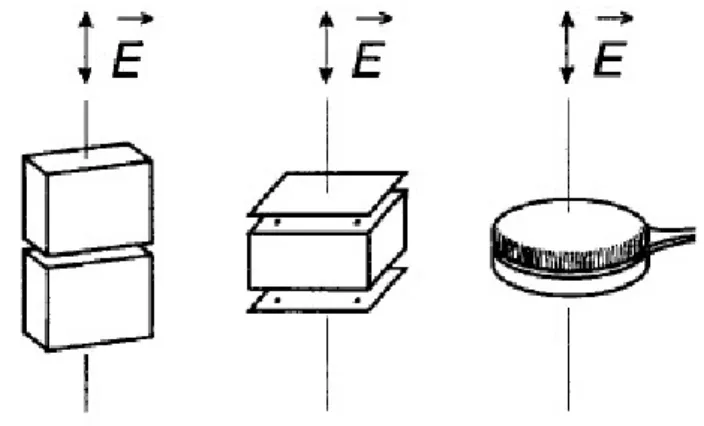
FIGURE 2-3 Geometries of commercial single-axis, free-body electric field meters. ... 54
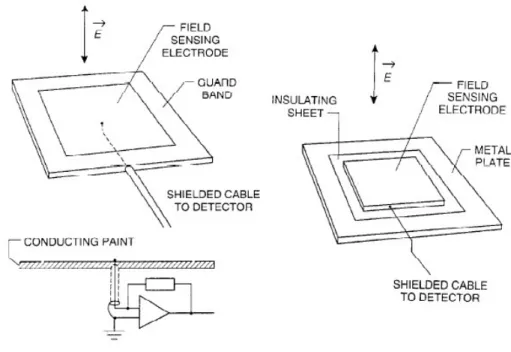
FIGURE 2-4 Two designs for flat probes used with ground-referenced electric field meters. ... 57
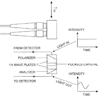
FIGURE 2-5 Probe for Pockels-effect electric field meter. ... 59
FIGURE 2-6 Working principle of the Kelvin probe. ... 61
FIGURE 2-7 Vibrating-reed meter. ... 62
FIGURE 2-8 Vibrating wire meter with conditioning circuit. ... 63
FIGURE 2-9 Laterally vibrating Kelvin probe. ... 65
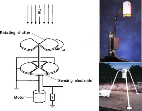
FIGURE 2-10 Simplified Schematic View of a Shutter-Type Electric Field Mill and two commercial devices. ... 67
FIGURE 2-11 Field mill operation [23]. ... 67
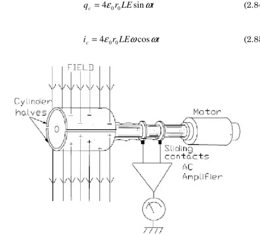
FIGURE 2-12 Schematic View of a Cylindrical Field Mill. ... 69
FIGURE 2-13 Schematization of the conditioning circuit for Kelvin probe. .... 71
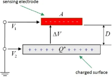
FIGURE 2-14 Dependence of the resolution on the distance of the sensing electrode from the charged surface. ... 72
FIGURE 2-15 Shielding of the sensing electrode with guard ring. ... 73
FIGURE 2-16 Schematic View of Vibrating Plate Electric-Field Meter Probe. ... ... 74
FIGURE 2-17 Schematization of a DC-feedback electrostatic voltmeter. ... 77
FIGURE 2-19 Measured voltage vs distance for field meter and AC feedback
ESVM. ... 79
CHAPTER 3 FIGURE 3-1 The first published hysteresis curve [80]. ... 89
FIGURE 3-2 Piezoelectric activity of Rochelle salt vs. temperature indicates the existence of two phase transitions [91] ... 90
FIGURE 3-3 The BaTiO3 crystal structure above (a) and below (b) the phase transition between cubic and tetragonal. ... 94
FIGURE 3-4 Direct and converse piezoelectric effects. ... 102
FIGURE 3-5 Point Groups classification of crystals. ... 104
FIGURE 3-6 Ferroelectric hysteresis loop [111]. ... 106
FIGURE 3-7 Ferroelectric domain walls in a perovskite ferroelectric. A-A’ lines represent 90° domain walls, and the B-B’ line a 180° domain wall (the tetragonality is highly exaggerated) [115]. . 109
FIGURE 3-8 Polarization versus Electric field loop behavior of a ferroelectric material. ... 110
FIGURE 3-9 The poling process schematization: (a) random orientation of polar domains prior to polarization; (b) polarization DC electric field; (c) remnant polarization after electric field removed. .... 111
FIGURE 3-10 (a) Fatigue; (b) Imprint; (c) Retention loss. ... 115
FIGURE 3-11 Schematic diagram of the ABO3 perovskite structure... 116
FIGURE 3-12 Lattice parameters of BaTiO3 as a function of temperature. .. 117
FIGURE 3-13 Dielectric constants of BaTiO3 as a function of temperature. 117 FIGURE 3-14 Crystallographic changes of BaTiO3. ... 118
FIGURE 3-15 (a) Phase diagram and (b) lattice constants of Pb(Zr,Ti)O3 solid solution. ... 121
FIGURE 3-16 Phase-Temperature diagram of PLZT as a function of %La. .. 123
CHAPTER 4 FIGURE 4-1 (a) Ferroelectric hysteresis loop, and, (b) the corresponding potential energy function that underpins the dynamics. ... 133
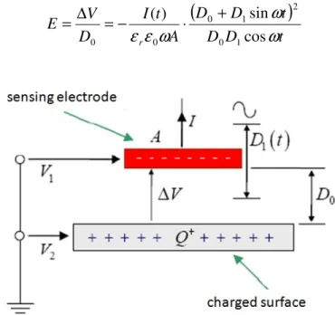
FIGURE 4-2 Oscillations: potential well function vs. the coupling λ. ... 134 FIGURE 4-3 Schematic of the Sawyer-Tower conditioning circuit where the “sensing” electrode in the CFE capacitor, used to induce the
perturbation ∆P in the ferroelectric polarization status, is highlighted. ... 135 FIGURA 4-4 Schematization of the structure of the ferroelectric capacitor used to sense an external electric field Ex. It is a parallel-plate capacitor having as dielectric a ferroelectric material and hosting in the upper electrode a third separated central “sensing” electrode used to convey the charges induced by the target electric field on the “charge collector” to the ferroelectric. The bottom and the upper outer driving electrodes are used to produce a bias polarization in the ferroelectric... 137 FIGURA 4-5 A typical Sawyer-Tower output voltage signal where the amplitude modulation of the reference signal is a result of the applied (target) low frequency signal. ... 138 FIGURA 4-6 A schematization of the charge collection strategy. ... 141 FIGURA 4-7 Schematization of the coupled circuit with N=3 elementary cells. ... 143 FIGURE 4-8 Schematization of the work flow required to simulate the behavior of a ferroelectric sensor. ... 146 FIGURE 4-9 The Penn State ferroelectric capacitor: (a) a real view of the prototypes together with a detailed view of the material layers, (b) a microscope picture of the ferroelectric sample and (c) a schematic of the bonding between the plates of the capacitors and the pins of the hosting package. ... 147 FIGURE 4-10 Device schematic wherein the dashed line outlines the ferroelectric capacitor in which two large top driving electrodes are used to polarize the ferroelectric “sensing region”. The small electrode in the middle (“the sensing electrode”) is wired to a “charge collector” that collects the charges induced by the target electric field. ... 148 FIGURE 4-11 A view of the meshed device including a shielding chamber and the charge collector (a), and a zoom of the sensor region (b)... 149 FIGURE 4-12 Qualitative FEM analysis of the ferroelectric capacitor without (a) and with (b) a perturbing action produced through the sensing electrode... 150
FIGURE 4-13 Experimental and theoretical (dashed line) hysteresis loops for driving voltages having amplitudes of (a) 10 Vpp and (b) 50 Vpp with frequency of 100 Hz. ... 153 FIGURE 4-14 GUI of the identification tool. ... 154 FIGURE 4-15 (a) Graphic representation of the spice model for the ferroelectric capacitor. (b) Spice implementation of the ferroelectric capacitor. ... 156 FIGURE 4-16 (a) Sawyer-Tower circuit simulated in the PSPICE environment; (b) Typical simulation results, highlighting the device behavior in the absence (blue line) and in the presence (red line) of a target electric field. A typical relationship between the target field and the perturbation ∆P has been adopted. ... 158 FIGURE 4-17 (a) An example of the polarization signal obtained by simulating (13) for a driving voltage of 10 Vpp and considering a target electric field having amplitude 14.29 V/m @ 10 Hz. The electric field produces a “modulation” (whose depth depends on the intensity of the target field) of the output signal. (b) Linear interpolation of the peak-to-peak modulation amplitude for three values of the target electric field with three different charge collectors (CC1, CC2 and CC3); the model predicts increasing device sensitivity with increasing size of the charge collector. The solid lines are for a driving voltage of 10 Vpp, while the dashed-lines are for a driving voltage of 50 Vpp. ... 159 FIGURE 4-18 The PSPICE model circuit with the ferroelectric capacitor. ... 161 FIGURE 4-19 An example of the output voltage signal of the PSPICE model in Figure 4-18 showing the effect of the perturbation on the third electrode of the ferroelectric capacitance ... 161 FIGURE 4-20 The linearity feature relating the Vout amplitude modulation with different ∆P. ... 162 FIGURE 4-21 Experimental setup. The two large electrodes (2 m x 2 m each) and the guard chamber are shown in (a); the charge collector is visible in (b). ... 163 FIGURE 4-22 (a) and (c) Sawyer-Tower circuit output signals for driving voltages amplitude of 10 Vpp @ 100 Hz and a target E field of
14.29 V/m @ 5 Hz and 10 Hz respectively; (b) and (d) voltage signals from the ST circuit after low-pass filtering and removal of mean value. ... 165 FIGURE 4-23 Power spectral density plots of the ST output signals for the cases of a driving (i.e. reference) signal of 10 Vpp @100 Hz and a target electric field at 5 Hz (a) and 10 Hz (b). Zooms are given in (c) and (d). The legend on each graph shows the amplitudes of the target electric field. ... 166 FIGURE 4-24 Linear interpolation of the peak-to-peak values of the output signals obtained with the various “charge collectors” and a target electric field having frequency of (a) 5 Hz and (b) 10 Hz. The energy barrier is U0 =5.3812e−6C/m2 ... 167 FIGURE 4-25 The ratio between the variation of the polarization P and the variation of the target electric field (this ratio provides a measure of the device efficiency) as a function of the ratio between the two areas S1 and S2. Square symbols and star symbols are used for a driving signal of 10Vpp@100Hz and 50Vpp@100Hz, respectively. A linear interpolation is also shown as used to estimate parameters θ1 and θ2; only the data not affected by saturation have been considered. ... 170 FIGURE 4-26 (a) A microscope image of the die with the capacitors in the outer ring (the central part of the die hosts other test structures and it is not of interest for us); (b) A schematization of the investigated capacitors. The size of the capacitor is 220µm x 220µm. ... 172 FIGURE 4-27 (a) A schematization of the Radiant's technology with the layers name indicated; (b) A simplified schematization of the same technology with indicated the thickness and the material used for each layer. ... 173 FIGURE 4-28 Schematization of the structural modification of the top electrode of the capacitor needed to realize the sensing electrode. ... 174 FIGURE 4-29 Ferroelectric capacitors produced by Radiant Technologies after the modification by the FIB of the top electrode. (a) three modified capacitors; (b) and (c) zoom of a single capacitor. The
disc in the central part of the sensing electrode is the zone in which the passivation has been removed to the purpose to electrically contact the electrode. ... 174 FIGURE 4-30 The electronic implementing the Sawyer-Tower circuit together with the DIP-28 package hosting the ferroelectric capacitors fabricated by Radiant Technologies Inc. ... 176 FIGURE 4-31 Examples of experimental P-E hysteresis (red line) for three amplitudes and two frequencies of the driving voltage together with the hysteresis predicted by the model (4.8) with the identified parameters (blu dotted line). ... 177 FIGURE 4-32 (a) The ferroelectric capacitor with the ST circuit under the microscope to contact the sensing electrode by a micro-tip; (b) A microscope image showing the capacitor and the tip contacting the sensing electrode; (c) An example of perturbed ST output voltage after applying a potential to the tip. ... 180 FIGURE 4-33 Effect on the ferroelectric hysteresis of the potential applied to the micro-tip by the signal generator used to mimic an external target E-field. ... 182 FIGURE 4-34 Examples of Sawyer-Tower output voltage signals for a driving volatge of 6 Vpp @510Hz of the driving voltage and for two amplitudes of the potential applied to the tip (a) 1V and (b) 500mV) at the frequency of 10 Hz... 183 FIGURE 4-35 Examples of PSD together with a zoom in correspondence of the frequency of the disturbing potential. ... 184 FIGURE 4-36 A comparison of the peak amplitude of the PSD at 1 Hz (a) and 10 Hz (b) for various amplitudes of the potential applied to the sensing electrode and a driving voltage of 6 Vpp @ 510 Hz and 1 kHz. ... 185 FIGURE 4-37 Trend of the PSD amplitude at the frequencies of 1 Hz and 10 Hz for various amplitudes of the potential applied to the micro-tip and driving voltage of 6 Vpp at the frequencies of 210 Hz, 510 Hz and 1 kHz. ... 185 FIGURE 4-38 The wafer with all the designed structures. The upper side of the wafer is dedicated to the ferroelectric capacitors while in the
bottom side others devices (MEMS suspend structures) have been placed. ... 188 FIGURE 4-39 Examples of layout of the capacitors. Four capacitors with different sizes of the top driving electrode and of the sensing electrode are shown. In (a) the driving and sensing electrodes are highlighted together with the relation between the sizes indicated in the upper part of the die and the geometrical features. The binary code in the bottom right corner of the die allows to univocally recognize the position of the capacitor on the wafer. ... 190 FIGURE 4-40 Microscope image of a capacitor and zoom of the regions where metal stripes bond the two driving electrode and the sensing electrode. ... 191 FIGURE 4-41 Schematic of the four-lead TO-18 header used to package the die with the single capacitor showing the pin assignment. .... 191 FIGURE 4-42 The TO-18 packaged capacitors. ... 192 FIGURE 4-43 Examples of experimental P-E hysteresis (red line) for three amplitudes and two frequencies of the driving voltage together with the hysteresis predicted by the model (4.8) with the identified parameters (blu dotted line). ... 194 FIGURE 4-44 Trend of the parameters a, b, and c for the capacitor C3 designated as 235-150-50 (red cap) as a function of the amplitude ((a), (c) and (e)) and frequency ((b), (d) and (f)) of the voltage applied to the driving electrodes. ... 196 FIGURE 4-45 Comparison for three capacitors (C2, C3, C4) designated as 235-150-50 (red cap) from the same group (i.e. having the same binary code 0001) as a function of the amplitude ((a), (c) and (e)) and frequency ((b), (d) and (f)) of the voltage applied to the driving electrodes. ... 198 FIGURE 4-46 Schematization of the sensor and the conditioning electronics. CFE and Cf (1.2nF) represent the ferroelectric capacitor and the feedback capacitor respectively, while Rf (2.7MΩ) is used to avoid the drift in the circuit output. ... 199 FIGURE 4-47 The setup used to generate the target E-field and the charge collector. Two sheet electrodes of 50cm x 50cm separated by
10cm, are used to generate a uniform electric field (distance between electrodes can be regulated as you need). Three charge collectors, CC1, CC2 and CC3 having dimensions 9cm x 9cm (the one shown in the picture), 20,5cm x 16cm and 25,5cm x 25,5cm have been used to collect the charges induced by the E-field. ... 200 FIGURE 4-48 Examples of experimental ST output voltages signal obtained by a driving signal of 6Vpp @ 1kHz and a target electric field of 200 V/m @ 100 Hz and 100 V/m @ 100 Hz. The effect of the target E-field is clearly visible. ... 201 FIGURE 4-50 The power spectral density (PSD) in the range (0 -1.2 kHz) of the ST output voltage when no external target E-field is present (Ex = 0V/m) in both the cases without (a) and with (b) the charge collector linked to the sensing electrode. In the latter case a peak in the PSD (see zoom in (b)) appears at 50Hz due to the electromagnetic smog in the environment. ... 203 FIGURE 4-51 Examples of the PSD in the range (0 - 1.2kHz) of the ST output voltage signal for four amplitudes of the target electric field: (a) 10V/m, (b) 50V/m, (c) 100V/m and (d) 200V/m, at 100Hz, having fixed a driving voltage of 6Vpp @ 1kHz. A stronger target signal enhances the height of the peaks at 100Hz in the PSD. ... 204 FIGURE 4-52 Comparison of the peaks of the PSD (V/Hz) of the ST output voltage for target electric fields @10Hz (a) and 100Hz (b) for the three charge collectors CC1, CC2 and CC3. ... 205 FIGURE 4-53 Schematic of the electronic implementing the coupled circuit. .... ... 207 FIGURE 4-54 Schematic of the electronic implementing the elementary cell and the coupling gain block. ... 208 FIGURE 4-55 PCB implementing the coupled circuit with N=3 cells. Ferroelectric capacitors (yellow caps) are easy to recognize in the upper part of the picture. ... 208 FIGURE 4-56 Examples of experimental signals for different values of the gain K. A decrease of the frequency of oscillation is observed increasing the gain. ... 210
FIGURE 4-57 Comparison of the main peaks of the PSD at the frequency of the oscillation for five values of the gain K. A shift in the frequency is clearly visible. ... 211 FIGURE 4-58 Trend of the frequency of the oscillations as a function of the gain K = [1+(R2/R1)]. ... 211 FIGURE 4-59 Effect of the charge collector. (a) zoom in the range 0 -200 Hz of the PSD of the output voltage of a cell of the coupled circuit with and without the charge collector. No external target E-fields was generated. A peak in the PSD at 50Hz, due to environmental electromagnetic fields, appears when the charge collector is connected. (b) comparison of the peak of the PSD at 50 Hz for five values of the gain K and for the same charge collector CC3... 214 FIGURE 4-60 Examples of the output signals of a cell of the circuit for two values of the amplitude 50 V/m (a) and (b) and 100 V/m (c) and (d) and two values of the frequency 500Hz (a) and (c) and 1kHz (b) and (d) of the target electric field. Superimposed to the main oscillations of the circuit (high frequency) a low frequency perturbation at the frequency of the target E-field is clearly visible. The amplitude of this perturbation (which resemble an amplitude modulation) is proportional to the E-field intensity. In addition to the target E-field another field at 50Hz is always detected and its effect is visible as a second order low frequency perturbation. This latter component can be easily removed by filtering the voltage signal ... 215 FIGURE 4-61 A comparison of the peaks of the PSD at 500Hz for all the amplitudes of the target E-field with the charge collectors CC1 (a) and CC2 (b) and K = 2. ... 216 FIGURE 4-62 Comparison of the peaks of the PSD for two frequencies of the target E-field 100Hz (a) and 500Hz (b) with the three charge collector for K = 2. A linear relationship between the amplitude of the target E-field and the peaks of the PSD (converted in V/√Hz) of the voltage output signals at the frequency of the target E-field can be arose from. The values of the parameters (α, β) of the linear interpolation are reported in Table 4-9. ... 218
FIGURE 4-63 Comparison of the peaks of the PSD at 100Hz with the three charge collector and for K = 3 (a) and K = 5 (b). ... 219
APPENDIX
LIST OF TABLES
CHAPTER 2
TABLE 2-1 Main parameters of vibrating-wire field meter ... 64
CHAPTER 3
TABLE 3-1 Differences between normal and relaxor ferroelectrics. ... 125 CHAPTER 4
TABLE 4-1 Model parameters derived by the Nelder-Mead optimization algorithm. ... 153 TABLE 4-2 Settings used in the characterization of the device with a target electric field. ... 164 TABLE 4-3 Parameters related to the linear interpolation indicated in (4.32). ... 168 TABLE 4-4 Evaluation of noise floor for two frequencies of the electric field (5 Hz and 10 Hz) and two amplitudes of the driving voltage (10 Vpp and 50 Vpp) ... 169 TABLE 4-5 The parameters identified for the capacitor C6 of the package 2 for different amplitudes and frequencies of the driving voltage. .. ... 178 TABLE 4-6 Summary of sizes of the oxide masks and platinum areas of the two driving electrodes and color of the paint applied to the metal cap for the identification of the capacitor. ... 192 TABLE 4-7 The parameters identified for the capacitor C3 designated as 235-150-50 (red cap) for different amplitudes and frequencies of the driving voltage. ... 195 TABLE 4-8 Parameters related to the linear interpolation of the peaks of the PSD shown in Figure 4-50. ... 206
TABLE 4-9 Parameters related to the linear interpolation of the peaks of the PSD at 100 Hz, 500 Hz and 1kHz for the three charge collector CC1, CC2, CC3 and a coupling gain K = 2. ... 220 TABLE 4-10 Parameters related to the linear interpolation of the peaks of the PSD at 100 Hz for the three charge collector CC1, CC2, CC3 and for K = 3, K = 4 and K = 5. ... 220
CHAPTER
1
An experiment is a question whichINTRODUCTION
science poses to Nature, and a measurement is the recording of Nature's answer. - Max Planck You make experiments and I make theories. Do you know the difference? A theory is something nobody believes, except the person who made it. An experiment is something everybody believes, except the person who made it. - Albert Einstein
Ferroelectric materials are defined as those which exhibit, at temperatures below the Curie point, a domain structure and spontaneous polarization which can be reoriented by applied electric fields. The domain morphology results from the alignment of dipoles to minimize electrostatic and elastic energy, and materials with this structure will exhibit varying degrees of hysteresis at all drive levels. Research and development in ferroelectric materials has advanced at an unimaginable rate in the past decade, driven mainly by three factors: new forms of materials, prepared in a multitude of sizes [1] (e.g. bulk single crystals and ceramics, nano-structured films, tubes, wires and particles) by a variety of techniques [2] (e.g. melt growth, physical
34 CHAPTER 1
deposition and to soft chemical synthesis); novel and intricate structural and physical properties have been discovered in these materials [2] (e.g. morphotropic phase boundary and related phenomena, domain engineering under fields, effects of nanostructures and superlattices); and the extraordinary potential offered by these materials to be used in the fabrication of a wide range of high-performance devices [3] (such as sensors, actuators, medical ultrasonic transducers, micro electromechanical systems (MEMS), microwave tuners, ferroelectric non-volatile random access memories (FeRAM), electro-optical modulators, etc.).
Ferroelectrics can be utilized in various devices such as high-permittivity dielectrics, pyroelectric sensor, piezoelectric devices, electrooptic devices and PTC components. The industries are producing large amounts of simple devices, e.g. ceramic capacitors, piezoelectric igniters, buzzers and PTC thermistors continuously [3]. But until now ferroelectric devices have failed to reach commercialization in more functional cases. In the light sensor, for example, semiconductive materials are superior to ferroelectrics in response speed and sensitivity. Magnetic devices are much more popular in the memory field, and liquid crystals are typically used for optical displays.
Starting from these considerations and taking in account the solid background on nonlinear dynamical systems at DIEES of the University of Catania, a nonlinear dynamical system based on ferroelectric capacitors coupled into a unidirectional ring circuit is considered with particular interest for developing novel electric field sensors.
This thesis deals with the exploitation of ferroelectric material properties and nonlinear dynamics behavior with emphasis on the realization of an innovative transducer.
The focused approach is based on the exploitation of circuits made up by the ring connection of an odd number of elements containing a ferroelectric capacitor, which under particular conditions exhibits an oscillating regime of behavior. For such a device, an external target electric field interacts with the system thus inducing perturbation of the polarization of the ferroelectric material; this, the target signal can be indirectly detected and quantified via its effect on the system response.
INTRODUCTION 35
The research work carried out for this Ph.D. thesis has been divided in five chapters, including this introduction, as summarized below briefly:
CHAPTER 2 is divided into two main sections: in the first section physical notions about electric fields and dielectric materials are given while in the second section a review of traditional instrumentation to measure electric fields together with a state of art on E-field sensors applications is presented.
CHAPTER 3 deals with ferroelectric materials: starting with an historical introduction to ferroelectrics, some theoretical notions together with a review of more popular ferroelectric material is given. The chapter ends with a state of art on ferroelectrics applications.
CHAPTER 4 reports both theoretical and experimental results. The
theory underpinning the system investigated here is presented together with simulations and experimental results.
CHAPTER
2
2
ELECTRIC FIELD BASES
AND INSTRUMENTATION
The important thing is to know how to take all things quietly. - Michael Faraday
1. ELECTRIC FIELD BASES
1.1. ELECTRIC FIELD
The concept of an electric field (E-field) was introduced by Michael Faraday in nineteenth century to address a property that describes the space that surrounds electrically charged particles as shown in
Figure 2-1 or that which is in the presence of a time-varying magnetic field.
The electric field is a vector field with SI units of Newtons per Coulomb (NC−1) or, equivalently, Volts per meter (Vm−1). The strength E of the field at a given point is defined as the force F that would be exerted on a positive test charge q of 1 coulomb placed at that point; the direction of the field is given by the direction of that force
=
C
N
q
F
E
r
r
(2.1)38 CHAPTER 2
FIGURE 2-1 The electric field surrounding a positive and a negative charge.
The direction of the electric field is the same as the direction of the force it would exert on a positively-charged particle, and opposite the direction of the force on a negatively-charged particle.
Since like charges repel and opposites attract, the electric field tends to point away from positive charges and towards negative charges.
The fundamental equation which describes the force between two point charges is Coulomb's law [4]. The magnitude of the electrostatic force between two point electric charges Q1 and Q2 is directly proportional to
the product of the magnitudes of each charge and inversely proportional to the square of the distance between the charges
[ ]
N
r
Q
Q
F
2 0 2 14
πε
=
(2.2)where
ε
0 is a constant called the permittivity of free space, defined as
×
≈
≡
−m
F
c
12 2 0 0 08
.
854187817
10
1
µ
ε
(2.3)where
c
0 is the speed of light in free space whileµ
0 is the vacuumELECTRIC FIELD BASES AND INSTRUMENTATION 39
Based on Coulomb's law for interacting point charges, the contribution to the E-field at a point in space due to a single, discrete charge located at another point in space is given by the following
r r q E ˆ 4 1 2 0
πε
= (2.4)where q is the charge of the particle creating the electric force, r is the distance from the particle with charge q to the E-field evaluation point,
rˆ is the unit vector pointing from the particle with charge q to the E-field evaluation point,
ε
0 is the permittivity.The total E-field due to a quantity of point charges nq, is simply the
superposition of the contribution of each individual point charge
∑
∑
= = = = q q n i i i i n i i r r q E E 1 0 2 1 ˆ 4 1πε
(2.5)Alternately, Gauss's law allows the E-field to be calculated in terms of a continuous distribution of charge density in space
ρ
0
ε
ρ
= ⋅ ∇ E (2.6)where the symbol
∇
is used to represent the del operator (see section 3). Coulomb's law is actually a special case of Gauss's law, a more fundamental description of the relationship between the distribution of electric charge in space and the resulting electric field [4]. Gauss's law is one of Maxwell's equations, a set of four laws governing electromagnetic.Electric fields contain electrical energy with energy density proportional to the square of the field amplitude
2
2 1
E
u =
ε
(2.7)where
ε
is the permittivity of the medium in which the field exists, andE is the electric field vector. The total energy stored in the electric field in a given volume V is therefore
40 CHAPTER 2
∫
V E dV 2 2 1ε
(2.8)where dV is the differential volume element.
An electric field that changes with time (such as due to the motion of charged particles in the field) will also influence the magnetic field of that region of space. As they move, they generate magnetic fields, and if the magnetic field changes, it generates electric fields (see section 9). A changing magnetic field gives rise to an electric field
t A V E ∂ ∂ − −∇ = (2.9)
which yields Faraday's law of induction
t B E ∂ ∂ − = × ∇ (2.10)
where
∇
×
E
indicates the curl (or rotor) of the electric field. For more details see section 10.This means that a magnetic field changing in time produces a curled electric field, possibly also changing in time. The situation in which electric or magnetic fields change in time is no longer electrostatics, but rather electrodynamics or electromagnetics.
Thus, in general, the electric and magnetic fields are not completely separate phenomenon. For this reason, one speaks of "electromagnetism" or "electromagnetic fields".
1.2. ELECTRIC WORK AND VOLTAGE
Relationship (2.1) is valid when the electric charges creating the electric field are fixed and constant in time and the charge q on which the E-field exerts the force is also fixed or movable without perturbing the electric charges distribution [4].
The work of the force F on a displacement ds of the charge q is given by
ds E q ds E q ds F dW = ⋅ = ⋅ = cos
θ
(2.11)ELECTRIC FIELD BASES AND INSTRUMENTATION 41
where
θ
is the angle between the electric field E and the displacement ds. For a displacement from a position A to a position B over a path C1the electric work is given by
∫
=∫
⋅ =∫
⋅ =1 1 1
C dW C F ds q CE ds
W (2.12)
The last integral in (2.12), that is the ratio between the electric force and the charge is the line integral of the electric field E over the path C1
and defines the electric voltage between the two points A and B related to the path C1. Choosing another path C2 from the same points A and B
we will find a different electric work then a different value of the electric voltage.
For a closed path C constituted, for example, by the path C1 from A to B
and by the path C2 from B to A the work results to be
∫
⋅ =∫
⋅ +∫
⋅ =∫
⋅ −∫
⋅ = − = − CF ds C F ds FC ds CF ds C F ds W W W 1 2 1 2 1 2 (2.13) which in general is not zero. Taking in account the (2.1)ξ
q
ds
E
q
ds
F
W
C C⋅
=
⋅
=
=
∫
∫
(2.14)where
ξ
is the electromotive force.Not any electric force is conservative but this is the case of the electrostatic forces for which the (2.12) can be rewritten in terms of the difference of the values of a function of the coordinates
( )
B
f
( )
A
f
ds
E
B A⋅
=
−
∫
(2.15)The opposite of this function is named potential difference between the points A and B
∫
⋅
=
−
B A B AV
E
ds
V
(2.16)From relationships (2.14) and (2.16) it follows that for a closed path in the space where the electric field E is defined
∫
⋅ = = == E ds 0 , W qE 0
42 CHAPTER 2
1.3. THE E-FIELD AS POTENTIAL GRADIENT
The potential is a continues scalar function and derivable. For a displacement dr=dxux +dyuy +dzuz from a point A(x, y, z) to B(x+dx, y+dy, z+dz) the potential variation is
dz E dy E dx E dr E z y x V dz z dy y dx x V dV = ( + , + , + )− ( , , )=− ⋅ =− x − y − z
On the other hand for the total differential theorem
dz z V dy y V dx x V dV ∂ ∂ + ∂ ∂ + ∂ ∂ = (2.18)
and from the comparison of this last two equations it follows that
z V E y V E x V Ex y z ∂ ∂ − = ∂ ∂ − = ∂ ∂ − = , , (2.19)
which can be synthetically written as
V grad
E =− (2.20)
or altenatively, introducing the del operator
z y x u z u y u x ∂ ∂ + ∂ ∂ + ∂ ∂ = ∇ (2.21) as it follows V V grad E =− =−∇ (2.22)
As a consequence the (2.16) can be rewritten as
∫
∫
⋅
=
−
∇
⋅
=
−
B A B A B AV
E
ds
V
ds
V
(2.23)1.4. CAPACITY OF AN ISOLATED CONDUCTOR
The electric charge distributed on the surface Σ of a conductor far from other charged bodies is related to the surface density
σ
by the equation∫
′ ′ ′ Σ= x y z d
ELECTRIC FIELD BASES AND INSTRUMENTATION 43
Under the electrostatic conditions all the electric charges are fixed then inside the conductor the electric field is null. One important consequence of this condition is that the potential is constant in every point of the conductor: given two any points P1 and P2
∫
⋅ = ⇒ = = = − 2 1 1 2 0 2 1) ( ) 0 ( ) ( ) ( P P E ds V P V P V P V P V (2.25)therefore the surface of the conductor is equipotential. Moreover the charge distribution assuring this condition is one and only one [4]. If the charge q is changed to the value q´=mq also the density and the potential changes of the same quantity. It follows that the ratio between the charge and the potential of the isolated conductor does not changes as the charge changes
V q
C = (2.26)
this ratio is named capacity and depends only from the shape and the dimensions of the conductor and from the properties of the surrounding medium. The unit of measurement of the capacity is coulomb/volt also named farad whose symbol is F.
This equation is valid for every couple of conductors for which there is a complete induction; such a system is called capacitor and the two conductors are named armors. The ratio between the absolute value of the charge on one of the armors and the potential difference is called capacity of the capacitor
2 1 V V q C − = (2.27)
The capacity depends on the geometry of the armors and on the properties of the interposed medium.
1.5. CONNECTION OF CAPACITORS
A capacitor is essentially used to store electric charges; although the total charge is null it is separated in the two quantities +q and –q which
44 CHAPTER 2
for a capacitor are proportional to the potential difference between the armors. By suitable external conductive links it is possible to flow the negative charge from an armor to the other one so generating an electric current which discharges the capacitor.
In the following the configurations of connection of capacitors are faced together with the evaluation of the equivalent total capacity. The charges and the potential differences will be supposed to be constant in time but the results are valid even for variable quantities.
For the sake of convenience we will indicate with V the potential difference V1-V2 between the armors and with C both the capacitor and
its capacitance. The circuital symbol of a capacitor (regardless of the geometry of its armors) is shown in Figure 2-2a.
Capacitors in series
The schematic of the connection in series is shown in Figure 2-2b. Every capacitor is connected to the next by only one link: the potential difference V is applied to the extremes of the series. Due to the induction effect the charge in every capacitor of the series is the same
n n C q V C q V C q V = , = , L = 2 2 1 1 (2.28)
The total potential difference is given by the sum of the potential difference of every single capacitor
eq n n n
C
q
C
C
C
q
C
q
C
q
C
q
V
V
V
V
=
+
+
+
=
+
+
+
=
+
+
+
=
1
1
1
2 1 2 1 2 1L
L
L
(2.29) where n n eq n eq C C C C C C C C C C C = + + + = + +L+ L L 2 1 2 1 2 1 , 1 1 1 1 (2.30) The inverse of the equivalent capacitance of the series is the sum of the inverse of the capacitance of the singles capacitors.ELECTRIC FIELD BASES AND INSTRUMENTATION
(a)
FIGURE 2-1 Connection of capacitors. (a) The capacitor; (b)
Capacitors in parallel
The schematic of the connection in parallel is shown in Figure Every capacitor is connected to the next by both the two armors: the same potential difference
capacitor
q1
the total charge of the system is given by the sum of the charges of every single capacitor
q q q= 1 +
The equivalent capacitance of capacitance of the single
1.6. DIELECTRICS. THE DIE
Let to consider a charged and isolated parallel plates capacitor: the charge q0 distributed
armors, an electric field and a potential difference given by
where C0 is the capacitance
Imagine to insert a conductive plate with thickness armors without touching them
ELECTRIC FIELD BASES AND INSTRUMENTATION
(b) (c)
Connection of capacitors. (a) The circuital symbol of a capacitor; (b) Capacitors in series; (c) Capacitors in parallel.
Capacitors in parallel
The schematic of the connection in parallel is shown in Figure Every capacitor is connected to the next by both the two armors: the
tential difference V is applied to the armors of every single
V C q V C q V C = n = n = 1 , 2 2 , , 1 L
the total charge of the system is given by the sum of the charges of every single capacitor
(
C C C)
V C V qq2 +L+ n = 1 + 2 +L+ n = eq
The equivalent capacitance of the parallel is then the sum of the capacitance of the singles capacitors.
DIELECTRICS. THE DIELECTRIC CONSTANT
Let to consider a charged and isolated parallel plates capacitor: the distributed uniformly with density
σ
0 produces, between the an electric field and a potential difference given byh
E
C
q
V
E
0 0 0 0 0 0 0=
,
=
=
ε
σ
is the capacitance and h the distance between the armors. a conductive plate with thickness s<h among the t touching them: the potential difference between the
45
circuital symbol of a Capacitors in series; (c) Capacitors in parallel.
The schematic of the connection in parallel is shown in Figure 2-2c. Every capacitor is connected to the next by both the two armors: the is applied to the armors of every single
(2.31) the total charge of the system is given by the sum of the charges of
(2.32) the parallel is then the sum of the
Let to consider a charged and isolated parallel plates capacitor: the between the
(2.33) the distance between the armors.
among the : the potential difference between the
46 CHAPTER 2
armors decreases due to the electrostatic induction on both the faces of the plate of a density distribution
σ
0 with opposite sign to null the field inside the plate; outside the field does not change then0 0(h s) V
E
V = − < (2.34)
Repeating the experiment with an insulating material with the same thickness the potential difference decreases less than in the previous case. The potential difference decreases linearly with increasing of the thickness of the plate assuming the least value Vk when the insulating
material totally fills the space between the armors.
Faraday has demonstrated that the ratio between the potential difference V0 without insulating material and the least value of the
potential difference Vk is always greater than 1 depending only by the
material properties. The insulating materials having the property to reduce the potential difference between the armors and then the electric field are called dielectrics and the dimensionless ratio [4]
1
0>
=
kV
V
κ
(2.35)is named relative dielectric constant.
For the capacitor filled by the insulating the electric field is
0 0 0 0
κε
σ
κ
κ
=
=
=
=
E
h
V
h
V
E
k k (2.36)then reduced by the factor
κ
. The variation of the electric field due to the dielectric is 0 0 0 0 0 0 0 0 01
1
ε
σ
χ
χ
ε
σ
κ
κ
κε
σ
ε
σ
+
=
−
=
−
=
−
E
kE
(2.37)where
χ
=κ
−1 is the electric suscettivity of the dielectric. The capacitance is 0 0 0 0C
V
q
V
q
C
k k=
=
κ
=
κ
(2.38)ELECTRIC FIELD BASES AND INSTRUMENTATION 47
that is the capacitance of the capacitor fulfilled by an insulating is increased by the factor
κ
.1.7. DIELECTRICS POLARIZATION
In absence of an electric field the electrons of an atom are on average distributed symmetrically around the nucleus: it is represented as a negative charged cloud filling a region around the nucleus with a radius equal to the atom dimension (~10-10 m); the center of mass of the
negative cloud coincides with positive nucleus.
Under the effect of an E-field the center of mass of the negative cloud is moved in the opposite direction of the field while the positive nucleus is moved in the same direction of the field; an equilibrium position is reached when this effect is balanced by the attraction forces of the opposite charges. Named x the vector going from the centre of the negative charge to the nucleus the electric dipole moment can be defined as it follows
Zex
pa = (2.39)
where Z is the atomic number and e the charge of the electron. The phenomenon is called electronic polarization and vanishes when the E-field is annulled. Every atom gains a mean electric dipole moment <p> parallel and having the same direction of the E-field.
Considering a volume
∆
τ
containing∆
N
atoms, the resulting dipole moment is ∆p=∆N < p> and the dipole moment per unit of volume is> < >= < ∆ ∆ = ∆ ∆ = p N p n p P
τ
τ
(2.40)where n is the number of atoms per unit of volume. The vector P is called polarization of the dielectric. In most dielectrics P results to be proportional to the E-field according to the following relation [4]
E E
P=
ε
0(κ
−1) =ε
0χ
(2.41)Dielectrics obeying the rule (2.41) are called linear and are amorphous and isotropic materials.
48 CHAPTER 2
The electric field generated by static charges remains to be conservative even with polarized dielectrics. Also the Gauss’s law is valid provided that the charges due to the polarization are taken into account
0
ε
ρ
ρ
p E= + ⋅ ∇ (2.42)these charges are not free to move and are distributed with density
P d dqp p = =−∇⋅
τ
ρ
(2.43)then from the (2.42) it results
(
ε
)
ρ
ρ
ε
ε
0∇⋅E =∇⋅ 0E= −∇⋅P ⇒ ∇⋅ 0E+P = (2.44) Introducing the dielectric induction vector DP E D=
ε
0 + (2.45) it followsρ
= ⋅ ∇ D (2.46)it depends only from the free charges, if no free charges are present
0
=
⋅
∇ D
then vector field D is solenoidal, moreover it is not conservative [4].The polarization and the dielectric induction have the same unit of measurement that is that of the surface density of charge C/m2.
1.8. ISOTROPIC AND ANISOTROPIC DIELECTRICS From equation (2.41) and taking in account (2.45) it follows
(
)
E E EP E
D=
ε
0 + =ε
0 1+χ
=ε
0κ
=ε
(2.47)where ε is the absolute dielectric constant; and using (2.47) in (2.41)
(
κ
)
ε
ε
0 1D/ P = − that is D D Pχ
χ
κ
κ
+ = − = 1 1 (2.48)ELECTRIC FIELD BASES AND INSTRUMENTATION 49
In a linear (then isotropic) dielectric the dielectric induction, the electric field and the polarization are vectors parallel to each other [4].
If the linear dielectric is homogeneous, that is the density is constant, even the relative dielectric constant is constant everywhere and from (2.48) it follows D P= − ∇⋅ ⋅ ∇
κ
κ
1 (2.49) since in the dielectric there are not free charge∇ D
⋅
=
0
then0 = ⋅ −∇ = P p
ρ
(2.50)In a homogeneous linear dielectric the spatial density of polarization charge is null and the polarization charges are distributed only on the surface [4].
When the relative dielectric constant is not constant and changes from point to point, from (2.49) it follows
− ∇ ⋅ + ⋅ ∇ − = ⋅ ∇
κ
κ
κ
κ
1 1 D D P (2.51)Even if there are not free charges in the dielectric the divergence of P is not zero and depends on the gradient of function ( −
κ
1)/κ
− ∇ ⋅ − = ⋅ −∇ =
κ
κ
ρ
p P D 1 (2.52)For the anisotropic dielectric like crystals, generally the polarization P is not parallel to the electric field E and the relation between this two quantity is given by the following triad
(
)
(
)
(
x y z)
z z y x y z y x x E E E P E E E P E E E P 33 32 31 0 23 22 21 0 13 12 11 0χ
χ
χ
ε
χ
χ
χ
ε
χ
χ
χ
ε
+ + = + + = + + = (2.53)The nine numbers
χ
ij constitute the electric suscettivity tensor; actually they are six becauseχ
ij =χ
ji(
i ≠ j)
that is the tensor is50 CHAPTER 2
Not even the vector D is parallel to the field E. However in these materials there three characteristic directions named crystallographic axes or optical axes of the dielectric which are mutually orthogonal and along which E, P and D are parallel.
1.9. TIME-VARIABLE ELECTRIC AND MAGNETIC FIELDS The local properties of time-constant electric fields E and magnetic fields B are determined in the vacuum by the four Maxwell’s equations
j B B E E 0 0 , 0 0 ,
µ
ε
ρ
= × ∇ = ⋅ ∇ = × ∇ = ⋅ ∇ (2.54)where the sources are represented by the charge density
ρ
(
x
,
y
,
z
)
and the current densityj
(
x
,
y
,
z
)
both constant in time. The steady state condition is underlined by the fact that in (2.54) do not compare the time derivation.The static and conservative E-field is generated by the fixed electric charges while the static magnetic field is generated by the electric charges in steady movement. Except that the sources of the static fields are the electric charges there is not any other relation between static electric and magnetic phenomenon.
A different relation between electricity and magnetism has been highlighted by Faraday and (separately) Henry’s experiments: a time-variable magnetic field produces a not conservative electric field which in suitable devices can generate an electromotive force or a current in a closed circuit; the same effect can be highlighted when a circuit moves respect a constant magnetic field. Subsequently Maxwell have demonstrated that a time-variable electric field generates a magnetic field reaching a more general form of the equations regulating the variable electric and magnetic phenomenon having the (2.54) as the particular static case. The fundamental results is that variables electric and magnetic fields can’t exist separately but have to be bring together under the more general concept of the electromagnetic field.
ELECTRIC FIELD BASES AND INSTRUMENTATION 51
1.10. FARADAY’S LAW
Experiments conducted by Faraday have demonstrated that whenever the flux of the magnetic field Φ(B) concatenated with a circuit changes in time it induces in the circuit an electromotive force given by
dt B d i ) ( Φ − =
ξ
(2.55)that is called Faraday’s law of the electromagnetic induction. The effect of the induced electromotive force is such to oppose to the generating phenomenon, this statement is known as Lenz’s law [4].
By the definition of electromotive force and magnetic flux it follows
∫
=−∫
Σ ⋅ Σ Φ − = ⋅ = B u d dt d dt B d ds Ei n i ) (ξ
(2.56)the variation of the magnetic flux concatenated with a closed path s generates an induced electric field Ei whose circuitation along s is
dt
d
Φ
/
−
. Then this field is not conservative. Σ is a surface having s as edge.The variation of the flux can be generated in different ways that can be classified in two main causes: the motion of a conductor in a reference system where the sources of the magnetic field are fixed and the time-variation of the magnetic field in a reference system in which the conductor is fixed. Focusing at this latter case let to reconsider the (2.56) moving the time derivation under the integration
∫
∫
Σ ∂ ⋅ Σ ∂ − = ⋅ = u d t B ds E n iξ
(2.57)Applying the Stokes’s theorem
∫
∫
Σ∫
Σ ∂ ⋅ Σ ∂ − = Σ ⋅ × ∇ = ⋅ u d t B d u E ds E n n (2.58)from which it follows that
t B E ∂ ∂ − = × ∇ (2.59)
52 CHAPTER 2
which express the local knot between the time-variation of the magnetic field and the induced electric field. This is one of the four Maxwell’s equations.
The magnetic field B can be represented as rotor of another vector A called potential vector then replacing in (2.59)
t A E t A A t E ∂ ∂ − = ⇒ ∂ ∂ × −∇ = × ∇ ∂ ∂ − = × ∇ (2.60)
In general the E-field can be generated even by fixed charges then its equation in terms of the scalar electrostatic potential and potential vector is V t A E −∇ ∂ ∂ − = (2.61)
ELECTRIC FIELD BASES AND INSTRUMENTATION 53
2. INSTRUMENTATION
2.1. INTRODUCTION
Sensors for electrostatic field [5] are employed in many applications either as stand-alone devices or as parts of more complex measurement systems (see section 11.3). Common applications concern surveying of fields generated by atmospheric phenomenon, transmission lines, particles detectors, mass spectrometers, scanning microscopes and electrophoresis systems [6], prevention of problems due to static charges either in processing and storage of inflammable materials and in the production of electronic devices. Automotive makes large use of such sensors for active and passive safety systems (such Air Bags), occupant sensing systems and touch controls [7]. Another interesting challenge pertain the areas of security and surveillance where they can be exploited to remotely detect weak biological fields produced by human bodies or animals.
Measurement of electrostatic fields requires the use of contactless systems to avoid surface discharging and potential alteration. Non-contacting instruments are commonly classified as electrostatic field meters (ESFM) and electrostatic voltmeters (ESVM).
2.2. ELECTROSTATIC FIELD METERS
Electrostatic field meters, also called static meters or static locators, measure the intensity of electrostatic field generated by a charged surface located some distance away using an high input impedance or chopper stabilized sensor that is referenced to ground. The sensor to surface distance must be known in order to obtain an accurate measurement; calibration of field meters must be performed before every measurement session [8], [5].
Electric field meters consist of two parts the probe or field sensing element and the detector which processes the signal from the probe and indicates the rms value of the electric field strength in units of V/m