4 Verification and Validation of the interface
4.1 Verification road map
According to the verification methodology and approach shown in the section 1.7 of the introduction, the validation of the I2C/SPI Interface has been performed at three verification levels:
1 Block- and Bus-Level Verification
– Registers test (reset, walking one, … )
– Communication tests (slave and master, TX/RX)
2. System-Level Verification
– Same tests as at Block and Bus levels, inside the Leon CVS Environment
3. Hardware emulation
– Same tests as at Block and Bus levels on the Memec Design FPGA prototyping board
4.1.1 Step 1: I
2C slave mode validation vs. an external I
2C master module
Our I2C/SPI interface has been first validated in I2C slave mode vs. a public available I2C master, whose behavioural HDL description can be found on www.opencores.org.
I2C Master scl sda I2C Slave I2C slave to validate 9 I2C master external by Opencores
The two interfaces have been linked on the I2C bus and then several tests (see conformance matrix in Table 4-1) have been performed. All the slave features are checked with positive results. The Slave mode validation model is shown in figure 4-1.
Figure 4-1: Slave mode validation model
4.1.2 Step 2: I
2C master mode validation vs. I
2C slave validated at step 1
After that the validation of the I2C/SPI interface in I2C master mode has been carried out vs. the I2C slave module validated at the Step 1 as shown in figure 4-2. The two interfaces have been linked on the I2C bus and then several tests (see conformance matrix in Table 4-1) have been performed. No difference has been detected on the behaviour of our I2C/SPI interface in I2C master mode with respect to the public available I2C master model.
Figure 4-2: Master mode validation model
I2C Slave I2C Master scl sda I2C slave validated at step 1 I2C master to validate 9
I2C slave validated at step 1 scl sda I2C Slave I2C master validated at step 2
9
I2C Master9
LEON CORE APB BUS4.1.3 Step 3: I
2C master and slave mode validation post synthesis
After the functional verification a timing verification has been performed. The I2C/SPI interface has been synthesized then the gate-level DUT has been feed with the same tests as at the previous steps and a design timing constraint check has been done.
Figure 4-3: Master and Slave post-syntheses validation model
4.1.4 Step 4: I
2C system validation within Leon CVS environment
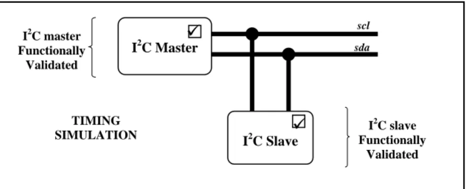
The last step has been the validation of the IP at system level within the Leon CVS environment as shown in figure 4-4. The I2C/SPI interface has been linked on the APB bus inside the Leon Core and then several tests files in SPARC-V8 assembly language have been written to check the functionalities of our interface. Many of the tests already executed at Block- and Bus- Level have been performed again at system level.
Figure 4-4: Leon environment validation model
I2C Slave I2C Master scl sda I2C slave Functionally Validated I2C master Functionally Validated 9 9 TIMING SIMULATION
Notes:
To perform the arbitration lost test the validation model of figure 4-9 (see section 4.2.3.3.1) has been used.
Our I2
C/SPI interface has been validated in SPI mode vs. the SD-SPI interface.
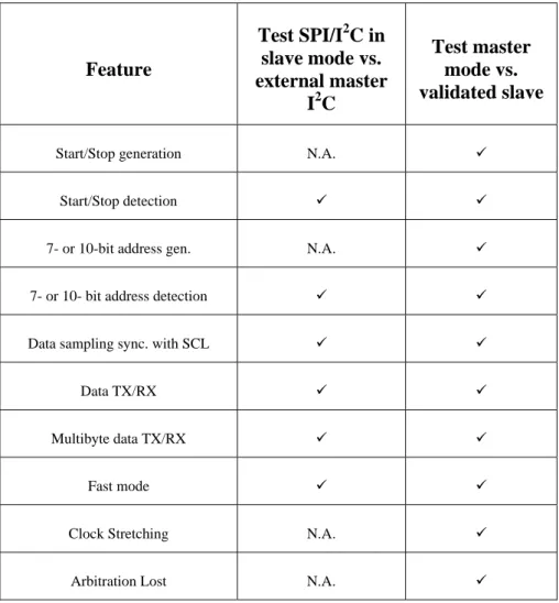
4.1.5 I2C standard conformance matrix
Table 4-1: Standard conformance matrix Feature Test SPI/I2C in slave mode vs. external master I2C Test master mode vs. validated slave
Start/Stop generation N.A. 9
Start/Stop detection 9 9
7- or 10-bit address gen. N.A. 9
7- or 10- bit address detection 9 9
Data sampling sync. with SCL 9 9
Data TX/RX 9 9
Multibyte data TX/RX 9 9
Fast mode 9 9
Clock Stretching N.A. 9
4.2 Main structure of the Test environment
4.2.1 Overview
In this section the structure of the test environment is given with a detailed explanation of the VHDL procedures used for the test bench at block- and bus-level and of the SPARC-V8 assembly language test drivers written to validate the IP into the Leon CVS. The attention is focused on the I2C module of the I2C/SPI Interface.
Table 4-2: I2C module features
Referring to section 2.5 the fundamental features of I2C are:
7- or 10-bit addressing modes.
Feature Slave Mode
Master Mode Start/Stop generation N.A. 9
Start/Stop detection 9 9
7- or 10-bit address gen. N.A. 9
7- or 10- bit address detection 9 9
Data sampling sync. with SCL 9 9
Data TX/RX 9 9
Multibyte data TX/RX 9 9
Fast mode 9 9
Clock Stretching N.A. 9
Clock stretching, wait state generation, bus busy and arbitration lost detection. Start/Stop/Repeated Start/Acknowledge generation and detection.
Data transmission and reception synchronous with SCL line Fast mode (up to 400 kbit/s)
Some of these characteristics are shared between slave and master modes; others are typical of the latter mode. Table 4-2 summarizes the main I2C module features.
4.2.2 Block- and Bus-Level Verification
4.2.2.1 Functional Verification
A functional verification of the I2C/SPI interface has been performed at block and bus level to check the compliance with the protocol of the I2C module
4.2.2.2
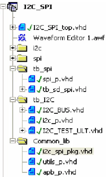
VHDL structure of the I
2C/SPI module and Test suite
The figure 4-5 shows the VHDL structure of the I2C/SPI module. The top of the I2
C/SPI interface is I2C_SPI_top.vhd. Folder i2c contains the VHDL source code for the I2
C IP Folder spi contains the VHDL source code for the SPI IP Folder tb_I2C contains the test bench files for the I2
C/SPI module in I2C mode:
o I2C_TEST_ULT reports test commands executed when running the I2Ctest o I2C_BUS reports the implementation of I2C BUS with resistive pull-up o I2C_p reports declarations and definitions of functions and procedures
Folder tb_spi contains the test bench files for the I2
C/SPI module in SPI mode:
o tb_sd_spi reports tests executed when running the SPItest bench o spi_p reports declarations and definitions of functions and procedures.
Folder common_lib contains common VHDL code:
o utils_p reports a package with several utilities to print messages in simulations
o apb_p reports functions and procedures to emulate the APB bus behaviour o I2c_spi_pkg reports utilities, registers addresses map and commands list
coding for the I2C/SPI module
The description of the test functions for the I2C/SPI module in I2C mode is reported in section 4.2.2.3.2 of this chapter and the summary of the tests executed by default is reported in section 4.2.2.3.3 Section 4.2.2.3.4 shows some case examples.
In order to modify the I2C test bench with respect to the default values of the current implementation the user shall modify the following files:
- i2c_test_ult.vhd: it reports the test bench commands from the user.
- i2c_spi_pkg.vhd: it reports registers addresses map and commands list coding.
As far as the test bench in SPI mode is concerned we keep the same structure of the test bench provided by SD.
By default the reset value for the sel_reg in I2C/SPI interface forces the interface working in SPI mode. The i2c_test_ult.vhd when executed provides to set properly the sel_reg to force the interface working in I2C mode.
4.2.2.3 Amba APB emulation
To drive the I2C/SPI interface and perform a Transaction-based verification an APB Bus Functional Model (BFM) has been created.
All possible operation types between the APB BUS master and the peripherals was emulated and systematically tested. The BFM drives signals on the interconnects according to the requirements of the interface protocols. Self-checking and directed random testing has been performed. Particularly the following functions were implemented:
• GET_APB_VALUE it performs an APB read access to a given register address and gives back the register value.
• APB_READ it performs an APB read access to a given register address and compares the expected result with the actual one, updating the 'error_flag' flag accordingly: in EQUAL mode, there is an error whenever the expected read data is different from the actual one, while in NOT_EQUAL one the two data have to be different.
• APB_WRITE it performs an APB write access to a given register address. The back verification is optional.
4.2.2.3.1 Read and check cycle
Hereafter an example of the Read and Check functions is shown:
-- Constant and types definitions for AMBA(TM) APB
constant PDMAX: Positive range 8 to 32 := 32; -- data width constant PAMAX: Positive range 8 to 32 := 16; -- address width type apb_slv_in_type is
record
PCLK_en: std_logic; -- PCLK enable
PSEL: std_logic; -- slave select
PENABLE: std_ulogic; -- strobe
PADDR: std_logic_vector(PAMAX-1 downto 0); -- address bus
PWRITE: std_ulogic; -- write
PWDATA: std_logic_vector(PDMAX-1 downto 0); -- write data bus
end record;
type apb_slv_out_type is record
PRDATA:std_logic_vector(PDMAX-1 downto 0); -- read data bus
end record;
type apb_slv_in_vector is array (natural range <> ) of apb_slv_in_type; type apb_slv_out_vector is array (natural range <> ) of apb_slv_out_type; constant my_delay : time := 2 ns;
constant comment_on : boolean := true; type verification_mode is (CHECK, NONE); type check_mode is (EQUAL, NOT_EQUAL); -- procedure name: APB_READ
procedure apb_read (
signal PCLK: : in std_logic;
signal apbi : out apb_slv_in_type;
signal apbo : in apb_slv_out_type; signal error_flag : inout std_logic;
variable apb_addr : in std_logic_vector(PAMAX-1 downto 0); variable mask : in std_logic_vector(PDMAX-1 downto 0); variable exp_apb_data : in std_logic_vector(PDMAX-1 downto 0);
mode : in check_mode
) is
variable apb_data : std_logic_vector(PDMAX-1 downto 0); begin -- SETUP
wait until PCLK'event and PCLK = '1';
wait for my_delay;
apbi.PADDR <= apb_addr;
apbi.PWRITE <= '0';
apbi.PSEL <= '1';
apbi.PCLK_en <= '0';
wait until PCLK'event and PCLK = '1'; -- ENABLE wait for my_delay;
apbi.PENABLE <= '1'; apbi.PCLK_en <= '1';
wait until PCLK'event and PCLK = '1'; -- CLOSE TRANSFER
apb_data:= apbo.PRDATA;
wait for my_delay; apbi.PSEL <= '0'; apbi.PENABLE <= '0'; apbi.PCLK_en <= '0';
--APPLY MASK and ERROR FLAG SET apb_data := apb_data and mask; -- the flag set depends on the MODE if (mode = EQUAL) then
if (exp_apb_data /= apb_data)then error_flag <= '1'; end if; else
if (exp_apb_data = apb_data) then error_flag <= '1'; end if; end if;
if comment_on then -- CHECK TEST RESULT if (mode = EQUAL) then
print_msg("action: READ trasfer");
print_msg("address: " & stdvect_to_str(apb_addr,16)); if (exp_apb_data = apb_data) then
print_msg("status: OK");
print_msg("value: " & stdvect_to_str(apb_data,16));
else
print_msg("status: FAILED");
print_msg("expected: " & stdvect_to_str(exp_apb_data,16)); print_msg("actual: " & stdvect_to_str(apb_data,16));
error_flag <= '1';
end if;
else
print_msg("action: READ trasfer to check difference"); print_msg("address: " & stdvect_to_str(apb_addr,16)); if (exp_apb_data = apb_data) then
print_msg("status: FAILED");
print_msg("value: " & stdvect_to_str(apb_data,16)); error_flag <= '1';
else
print_msg("status: OK");
print_msg("not expected: " & stdvect_to_str(exp_apb_data,16)); print_msg("actual: " & stdvect_to_str(apb_data,16)); end if;
end if;
print_msg(" "); end if;
4.2.2.3.2 Customizable Test functions
These functions are used to test I2C/SPI interface in I2C mode:
a. IP_reset (defined in apb_p.vhd and used in file I2C_TEST_ULT.vhd)
b. Walking_one_test (defined in i2c_p.vhd and used in file I2C_TEST_ULT.vhd) c. Default_value_test (defined in i2c_p.vhd and used in file I2C_TEST_ULT.vhd) d. i2c_setup (defined in i2c_p.vhd and used in file I2C_TEST_ULT.vhd)
e. i2c_RX (defined in i2c_p.vhd and used in file I2C_TEST_ULT.vhd)
f. i2c_TX (defined in i2c_p.vhd and used in file I2C_TEST_ULT.vhd)
g. stretching (defined in i2c_p.vhd and used in file I2C_TEST_ULT.vhd)
Hereafter the characteristics of each function are shown:
4.2.2.3.2.1 Reset test
IP_reset: it simply reset the peripherals for a given number of clock cycles IP_reset ( signal reset_n : out std_logic;
signal clk : in std_logic;
n_cycles : in integer );
Example of system reset for 1 clock cycle on master device:
IP_reset (sys_reset_n_m, sys_clk_m, 1);
4.2.2.3.2.2 Walking one test
Walking_one_test: it performs the walking one test for all registers on APB Bus Walking_one_test ( signal CLK : in std_logic;
signal CLK_APB : in std_logic;
signal apbi : out apb_slv_in_type;
signal apbo : in apb_slv_out_type;
signal error_flag : inout std_logic );
Example of walking one test on master device:
4.2.2.3.2.3 Default value test
Default_value_test: it performs the check of the default value in each register accessible
by the APB bus after the reset.
Default_value_test ( signal CLK : in std_logic;
signal CLK_APB : in std_logic;
signal apbi : out apb_slv_in_type;
signal apbo : in apb_slv_out_type;
signal error_flag : inout std_logic );
Example of default value test on master device registers:
Default_value_test (sys_clk_m, PCLK, apbi_m, apbo_m,error_flag_m);
4.2.2.3.2.4 Transfer setup
i2c_setup: it performs the transfer setup of the IP
i2c_setup ( signal clk_M : in std_logic;
signal clk_S : in std_logic;
signal clk_APB : in std_logic;
variable data:in std_logic_vector(PDMAX-1 downto 0);
signal apbi_m : out apb_slv_in_type;
signal apbo_m : in apb_slv_out_type;
signal error_flag_m : inout std_logic;
signal irq_m : in std_logic;
signal apbi_s : out apb_slv_in_type; signal apbo_s : in apb_slv_out_type; signal error_flag_s : inout std_logic;
signal irq_s : in std_logic;
addressing_type : in addressing_mode; transfer : in transfer_mode; variable speed: in std_logic_vector(PDMAX-1 downto 0)
);
data is the slave address
addressing_type is Bit_10 or Bit_7: indicates the addressing mode
transfer is TX or RX : indicates if the IP must perform a data transmission (TX) or a reception (RX)
speed: indicates the data transfer rate
Example of 10 bit addressing RX:
Data := X"00_00_02_00";
i2c_setup ( sys_clk_m, sys_clk_s, PCLK, data,
apbi_m, apbo_m, error_flag_m,irq_m,
apbi_s, apbo_s, error_flag_s,irq_s,
bit_10, RX, speed);
4.2.2.3.2.5 Reception
i2c_RX : it performs the reception of n_bytes i2c_RX (
signal clk_M : in std_logic;
signal clk_S : in std_logic;
signal clk_APB : in std_logic;
signal apbi_m : out apb_slv_in_type;
signal apbo_m : in apb_slv_out_type;
signal error_flag_m : inout std_logic;
signal apbi_s : out apb_slv_in_type;
signal apbo_s : in apb_slv_out_type;
signal error_flag_s : inout std_logic; variable n_bytes : in integer;
transfer_type : in type_of_transfer;
variable data : in std_logic_vector(PDMAX-1 downto 0); variable speed: in std_logic_vector(PDMAX-1 downto 0)
);
n_bytes: number of bytes for each frame to transfer (1 to 4) transfer_type is (ACK, NACK, STO):
o ACK Æ Master gives acknowledge at the end of the transfer o NACK Æ Master doesn’t give acknowledge at the end of the
transfer; next action required is a new setup procedure. o STO Æ Master gives NACK and STOP
Data indicates data to transfer
Speed indicates data transfer speed (see section 1.5.2 of the I2
C/SPI user’s manual)
Example of 1 byte RX:
n_bytes:= 1;
Data:= X"F0_F4_74_81";
i2c_RX ( sys_clk_m, sys_clk_s, PCLK, apbi_m, apbo_m, error_flag_m, apbi_s, apbo_s, error_flag_s, n_bytes, ACK, data,
4.2.2.3.2.6 Transmission
i2c_TX: it performs the transmission of n_bytes i2c_TX (
signal clk_M : in std_logic; signal clk_S : in std_logic;
signal clk_APB : in std_logic;
signal apbi_m : out apb_slv_in_type;
signal apbo_m : in apb_slv_out_type;
signal error_flag_m : inout std_logic;
signal apbi_s : out apb_slv_in_type;
signal apbo_s : in apb_slv_out_type;
signal error_flag_s : inout std_logic;
variable n_bytes : in integer;
transfer_type : in type_of_transfer;
variable data : in std_logic_vector(PDMAX-1 downto 0); variable speed : in std_logic_vector(PDMAX-1 downto 0) variable str_time : in time
);
n_bytes: number of bytes for each frame (1 to 4) transfer_type is (ACK, STO);
o ACK Æ Slave gives acknowledge at the end of the transfer
o STO Æ Slave gives NACK and master generates STOP condition data: indicates data to transfer
speed: indicates data transfer speed (see section 1.5.2 of the I2
C/SPI user’s manual) str_time: indicates the duration of the stretching. It has to be set to "0 ns" when the
stretching test is not required
- Example of 1 byte transmission and stop
n_bytes:= 1;
data := X"F0_F4_77_F1";
i2c_TX (sys_clk_m, sys_clk_s, PCLK, apbi_m, apbo_m, error_flag_m, apbi_s, apbo_s, error_flag_s,
4.2.2.3.2.7 Stretching
stretching: it performs the stretching for str_time at the nbit-th of the transfer
stretching (
signal scl_pad_oe_n_s1 : out std_logic; variable nbit : in Integer; variable str_time :in time;
variable speed:in std_logic_vector(PDMAX-1 downto 0)
);
• nbit: Bit position at which the clock stretching be apply • str_time: stretching duration
• speed: indicates data transfer speed
This function can be used only before an i2c_TX procedure and the nbit is a number less or equal the number of bit transmitted in the referred i2c_TX.
- Example of stretching at the 13th bit for 10000 ns for a 3 byte transmission
nbit:= 13; -- Maximum number allowed is 27 str_time:= 10000 ns;
stretching (scl_pad_oe_n_s1, nbit,str_time,speed);
n_bytes:= 3;
data := X"99_F5_54_43";
i2c_TX (sys_clk_m, sys_clk_s, PCLK, apbi_m, apbo_m, error_flag_m, apbi_s, apbo_s, error_flag_s, n_bytes, ACK, data,
4.2.2.3.3 Summary of the tests executed by I2C test bench
Hereafter we report the order of the test executed when running the I2Ctest bench.
The following test has been used to extract the switching activity during power consumption estimation at gate level.
1. Reset
2. Default value test
3. Addressing 10 BIT, Mode: MASTER-RX
a. RX 1 bytes and ACK of the data received b. RX 2 bytes and ACK of the data received c. RX 3 bytes and ACK of the data received d. RX 4 bytes and ACK of the data received
e. RX 1 byte and NACK of the data received and STOP f. Addressing 10 BIT, Mode: MASTER-RX
g. RX 4 byte e NACK of the data received
4. Addressing 10 BIT, Mode: MASTER-TX a. Repeated start test
b. TX 1 bytes and ACK of the data received by slave c. TX 2 bytes and ACK of the data received by slave d. Clock stretching
e. TX 3 bytes and ACK of the data received by slave f. Clock stretching
g. TX 4 bytes and ACK of the data received by slave h. Arbitration lost CHECK
4.2.2.3.4 Some Case example
- A. Addressing 10 BIT, Mode: MASTER-RX
Speed := X"00_00_00_09"; -- 400 Kbit/sec Data := X"00_00_02_00";
i2c_setup( sys_clk_m, sys_clk_s, PCLK,
data,
apbi_m, apbo_m, error_flag_m,irq_m, apbi_s, apbo_s, error_flag_s,irq_s, bit_10, RX, speed);
I2C BUS
Scl_ms: SCL bus Sda_ms: SDA Bus
S: Start A1: ACK P: Stop NA: Not ACK Sr: Repeated start
M: Master Sl: Slave B: BUS
S A1 A2 Sr
M
Sl
B
- B. RX 1 byte and NACK of the data received and STOP
n_bytes:= 1; data := X"F0_74_74_81";
i2c_RX ( sys_clk_m, sys_clk_s, PCLK, apbi_m, apbo_m, error_flag_m, pbi_s, apbo_s, error_flag_s, n_bytes, STO, data, speed);
- C. TX 1 byte and ACK of the data received by slave and STOP str_time:= 0 ns; n_bytes:= 1;
data := X"F0_F4_77_F1";
i2c_TX ( sys_clk_m, sys_clk_s, PCLK,
apbi_m, apbo_m, error_flag_m,
apbi_s, apbo_s, error_flag_s,
n_bytes, STO, data,
speed, str_time); A P M Sl B NA P M Sl B
4.2.2.4 Timing Verification
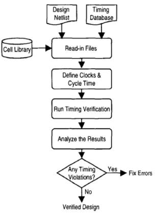
A timing verification of the I2C/SPI interface has been performed. Timing analysis uses simulation vectors to verify that the circuit or design outputs accurate results from a given input without any timing violations. Each storage element and latch in a design has timing requirements that have to be met. These include setup, hold, and various delay timings. A typical flow for a timing verification is shown in figure 4-6.
Figure 4-6: Typical flow for timing verification
4.2.2.4.1 Synthesis on CMOS of the I2C/SPI interface
For the synthesis of the interface the CORELIB8DLL_HCMOS8D technologic library, supplied by STMicroelectronics has been used. This library is a standard-cells library for VLSI projects with 0.18 µm technology. This library contains 574 cells between combinatorial and sequential, designed to work at 1.3 20%) and at 1.8 (+10%/-20%) Volt of supply.
4.2.2.4.1.1 Software tool
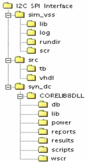
For the synthesis of the system with CMOS the program Synopsis has been used. This program makes large use of script files to make faster the procedure of synthesis. These files need a particular directory structure shown in figure 4-6:
Figure 4-7: Directory structure in Synopsis
The three principal directories are:
• “sim_vss”: it is the directory used for simulation pre- and post synthesis. o “scr” contains simulation scripts
o “log” containserror messages generated during compilation
o “lib” contains “.sim” and “.mra” files produced during vhdl analysis. • “src” contains “.vhd” files of the system.
o “tb” containstest-bench files.
• “syn_dc” it is the directory used for synthesis.
o “db”contains the “.db” files generated by synthesis
o “lib” contains “.mr”, “.st”, “.syn” filesproduced by “analyze” and “elaborate” commands.
o “power”directory contains files useful for power analysis.
o “reports”contains information on the project collected during thesynthesis and power analysis processes (like area, timing reports).
o “results” contains “.vhd” filesof the synthesized project, that are used in post-synthesissimulation.
o “scripts” contains the script files, usedfor the synthesis and the power analysis.
o The “wscr” contains scriptfiles of dc_shell commands to save the attributes of actual project.
4.2.2.4.1.2 Synthesis reports
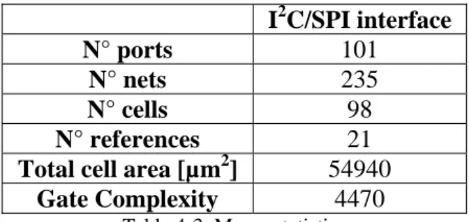
Hereafter the report generated will be shown. The most significant data reported are:
• Cell area information in µm2 and Gate-Equivalent area • Timing information, based on the critical path
Synthesis results have been obtained with a clock requirement of 20 MHz (typical of SPI and I2C applications) [18]. CMOS synthesis results demonstrate that the above specification is reached. Below are reported the macro statistics and area occupation for the I2C/SPI module. The gate complexity is calculated dividing the cell area for the basic NAND area (12,288 µm2) I2C/SPI interface N° ports 101 N° nets 235 N° cells 98 N° references 21
Total cell area [µm2] 54940
Gate Complexity 4470
Table 4-3: Macro statistics
Below is reported the timing information for HS library. For the LL library the speed penalty versus HS is 29 % (e.g. at 1.55 V and 85 °C max frequency is 106.7 MHz for LL instead of 150.2 MHz for HS).
Table 4-4: Timing information for HS library
4.2.2.4.2 Summary of the tests executed by I2C test bench
The same test bench as in the functional verification has been performed. (see section 4.2.2.3.3 for the summary). All the timing requirements of table 2-2 have been positive checked.
4.2.3 System-level verification
4.2.3.1 Data base structure within Branca-Leon CVS environment
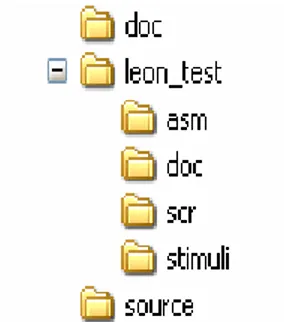
Hereafter it is shown the data base structure within Leon CVS environment:
Figure 4-8: Data base structure
Folder doc contains the documentation.
Folder source contains the VHDL source code for the I2
C/SPI interface:
o I2C_SPI_top.vhd is the top of the I2C/SPI interface o I2C_to_APB_top.vhd o i2c_master_byte_ctrl.vhd o i2c_master_bit_ctrl.vhd o sd_spi.vhd o sd_spi_pad_io.vhd o sd_spi_shift_reg.vhd o sd_spi_apb_if.vhd o sd_spi_clk_div.vhd o i2c_spi_pkg.vhd
Folder leon_test contains 3 folders:
o Folder asm contains assembly drivers for the tests: I2C
SPI
branca_I2C_SPI_reset_v001.S branca_I2C_SPI_walk1_v001.S branca_I2C_SPI_RX_v001.S branca_I2C_SPI_TX_v001.S branca_I2C_SPI_repeated_start_v001.S branca_I2C_SPI_arbitration_lost_v001.S
o Folder scr contains signals to be displayed by the waveform editor: branca_I2C_SPI_reset_v001 branca_I2C_SPI_walk1_v001 branca_I2C_SPI_RX_v001 branca_I2C_SPI_TX_v001 branca_I2C_SPI_repeated_start_v001 branca_I2C_SPI_arbitration_lost_v001
o Folder stimuli contains the signals provided for the test bench: branca_I2C_SPI_arbitration_lost_v001
default
o Folder doc contains a quick reference for the Assembler programmer: User_manual
4.2.3.2 Mounting of the new IP on AMBA on-chip APB bus
In order to mount the I2C/SPI interface on the AMBA on chip APB BUS inside the Leon core this VHDL files need to be modify:
Module containing the processor, caches, memory controller and standard peripherals. Here three instances of the I2C/SPI interface have been created, one master and two slaves connected through the I2C Bus.
• apbmst.vhd
AMBA AHB/APB Bridge. Here the mapping of the registers accessible by the AMBA APB bus has to be done.
Figure 4-9: Registers mapping on the AMBA APB BUS
• Leon.vhd
Top entity of the Leon processor. If some signal has to be driven out from the chip is necessary to modify here the instance of mcore and the entity Leon.
• Target.vhd
LEON target configuration package. Two constants has to be modified as shown below:
case apbaddr is . . . --- i2c_SPI master 0x100 - 0x120 when "01000000" | "01000001" | "01000010" | "01000011"| "01000100" | "01000101" | "01000110" | "01000111"| "01001000" => esel := '1'; bindex := 15; . . .
constant APB_SLV_MAX : integer := 18; -- maximum APB slaves
constant APB_SLV_ADDR_BITS : integer := 10; -- address bits to
4.2.3.3 Executed tests
Many of the tests already executed at Block and Bus levels have been performed inside the Leon CVS Environment.
Tests have been organized into several files which contain the assembler instructions to be executed. Hereafter an explanation of the contents of the test files is given:
branca_I2C_SPI_reset_v001:
It contains the assembly instructions for the reset test. First the check on the SPI registers accessible by APB bus has been performed (by default SPI mode is set after a reset event), then after a written on the sel_reg register to switch to I2C mode the same check has been performed on the I2C registers.
branca_I2C_SPI_walk1_v001:
It contains the assembly instructions for the walking one test. First the check on the SPI registers accessible by APB bus has been performed, then after a written on the sel_reg register to switch to I2C mode the same check has been performed on the I2C registers.
branca_I2C_SPI_RX_v001:
It contains the assembly instructions for a reception test with master in RX mode and slave in TX mode. The following tests are performed (just I2C mode) :
Addressing 10 bit
RX of 1 byte and ACK
RX of 1 byte and NACK and STOP Addressing 10 bit
RX of 3 bytes and ACK
branca_I2C_SPI_TX_v001:
It contains the assembly instructions for a transmission test with master in TX mode and slave in RX mode. The following tests are performed (just I2C mode):
Addressing 10 bit
TX of 1 byte and ACK TX of 2 bytes and ACK TX of 3 Bytes and ACK
TX of 2 bytes and ACK and STOP Addressing 10 bit
TX of 4 bytes and NACK and STOP branca_I2C_SPI_repeated_start_v001:
It contains the assembly instructions for a repeated start test. First the master is in RX mode and slave in TX mode, then the mode is switched to TX for the master and RX for the slave. The following tests are performed:
Addressing 10 bit, Mode: RX RX of 1 byte and NACK
Addressing 10 bit, Mode: RX (repeated start) RX of 3 bytes and NACK and STOP Addressing 10 bit, Mode: TX
TX of 1 byte and NACK
Addressing 10 bit, Mode: TX (repeated start) TX of 1 byte and NACK and STOP branca_I2C_SPI_arbitration_lost_v001:
scl sda LEON APB BUS I 2C Slave scl scl I2C Master 1 sda scl sda sda Scl_command a_lost_test 1 0 I2C Master 2
4.2.3.3.1 Arbitration lost test validation model
Since we have just one host processor that drives both the two I2C/SPI interfaces connected to the APB BUS the arbitration lost check can’t be performed simply.
This event in fact occur when two or more masters generate a START condition within the minimum hold time (tHD;STA) of the START condition which results in a defined
START condition on the bus. (See 1.8.2.3 of the user manual [16]).
This condition cant be emulate using the validation model of figure 4-4 because the processor through the APB bus uses three clock cycles to perform a writing on a register. So while the Leon is writing the start command in the command register of the second master, the first master has already asserted a Start condition on the I2C bus and it becomes the new master of the line.
Any other action on the bus is not allowed until a Stop condition is detected. To perform this test has been adopted therefore the validation model shown in fig. 4-10:
Figure 4-10: Arbitration lost validation model
The signal a_lost_test is used to enable the arbitration lost verification mode. When this mode is set, the signal scl_command becomes the controller of the scl bus. Using this control signal the scl bus is hold low (it emulates a wait state for the masters) and the
When the scl_command goes high the scl bus is released and the start command for both masters is executed at the same time and this allows testing the arbitration lost.
In the default executed test is the second master to lose the arbitration because it tries to drive high the sda line while the first master is driving it low.
In fact the master who transmits a HIGH level, while another master is transmitting a LOW level will switch off its DATA output stage because the level on the bus doesn’t correspond to its own level.
Because address and data information on the I2C-bus is determined by the winning master, no information is lost during the arbitration process.
An interrupt is set on the second master device when the arbitration lost event occurs.
The following tests are performed:
Master 1: Addressing 10 bit, Mode: RX (Bytes transmitted: F400) Master 2: Addressing 10 bit, Mode: RX (Bytes transmitted: F408)
-- Master 2 loses the arbitration -- RX of 2 byte and NACK and STOP
4.2.3.4 Some case examples
Hereafter some case examples are presented. For the function of each signal refer to section 2.5.4; the “m” in the signal name stands for “master”, the “s” stands for “slave”, the “s1” stands for “slave 1”. In the case of arbitration lost the “s” refers to the second master on the BUS.
Addressing 10 bit, Mode: RX RX of 1 byte and ACK
Addressing 10 bit, Mode: TX TX of 1 byte and ACK TX of 2 bytes and ACK
Addressing 10 bit, Mode: RX RX of 1 byte and NACK
Master 1: Addressing 10 bit, Mode: RX (Bytes transmitted: F400) Master 2: Addressing 10 bit, Mode: RX (Bytes transmitted: F408) Master 2 loses the arbitration –