POLITECNICO DI MILANO
SCHOOL OF INDUSTRIAL AND INFORMATION LAUREA MAGISTRALE IN MATERIALS ENGINEERING
AND
NANOTECHNOLOGY
Assessment of semi-conducting Carbon Nanotube networks for
fully printed field effect transistors
Supervisor: Prof. Chiara CASTIGLIONI
Co-supervisor: Dr. Mario CAIRONI
Prabir MAHATO
836126
i
ABSTRACT
Printed electronics is a branch of electronics where functional materials, such as conductors, semiconductors and dielectrics, are deposited one by one in the forms of inks with high-throughput printing machines inherited by the graphical arts. Printed electronics allows to add electronic functionalities with a cost-effective process on a wide variety of substrates, including plastic and paper, and it allows to target large-area electronics applications. Rather than competing with established silicon electronics, it offers alternative applications where lightweight, flexibility and ease of integration are critical figure of merits. Organic semiconductors, and in particular conjugated polymers, are typically considered among the best options for printed electronics, because of their chemical tunability, which simplifies inks formulations, their advantageous mechanical properties and electronic and optoelectronic properties which have improved over the last few decades.
However, semiconducting polymers still show limitations, both in terms of maximum field-effect charge carrier mobility, which is below 5 cm2V-1s-1 for most of largely available materials, and in terms of contact resistance, owing to high energetic barriers for injection of carriers from most of printable electrodes, thus complicating downscaling of devices. Both limitations represent a strong bottleneck for improvement of switching performances of printed electronics devices, such as printed transistors, therefore strongly limiting the overall expected speed of a printed polymer circuit. With the aim to find alternatives to printed polymers to overcome their current limitations, this work has the goal of assessing the use of semiconducting single-walled carbon nanotubes (swCNTs) for the fabrication of fully printed field-effect transistors on plastic substrates. While CNTs offer in principle much better electronic performances than polymers, especially in terms of charge mobility, economically viable methodologies to produce them lead to mix of conducting and semi-conducting nanotubes. Moreover their dispersion in suitable solvents to formulate stable, printable inks is still a challenge. One possible solution to both criticalities is to adopt polymer wrapping, where a semiconducting polymer capable of selectively wrapping specific chiralities can be used both as a sorting agent and a dispersant. The formulations of polymer wrapped swCNTs studied here have been provided by the group of Prof.
ii
M.A. Loi at the University of Groningen. An optimization of inkjet printing of swCNTs formulations has been performed in order to control the formation of suitable nanotubes networks. These printed networks were integrated in field-effect transistors printed on plastic by combining only inkjet printing and bar-coating in ambient air, demonstrating working devices with holes field-effect mobility reaching 1.90 cm2V-1s -1
. The obtained result is a first promising step towards high performance, fully printed CNTs based flexible circuits, which can be achieved by further optimization of the quality of the printed CNTs networks, especially in terms of coverage.
iii
ACKNOWLEDGEMENT
It was a great opportunity to work on my thesis at Center for Nano Science and Technology(CNST), under Italian Institute of Technology, Milano, Italy. I give my heartfelt thanks to Dr. Mario Caironi, Track Tenure Researcher at CNST, Milano and Prof. Chiara Castiglioni, professor at Politecnico Di Milano to provide me such an enriching environment to learn. Discussions with them on regular basis on the progress of my work were highly fruitful and provided me insight to my work.
I am thankful to Francesca Scuratti, PhD student at CNST, for her guidance, time and patience. As a master’s student, mostly having theoretical knowledge, she played an important role to translate it into the practical space in these nine months. I thank Matteo Cesarini, Diego Nava, Michele Garbugli and others from the CNST lab for their extended support whenever required during different stages of my work.
Lastly, I thank my beloved parents, Smt. Ahalya , Shri Harendra Kr. Mahato and my dear sister Jyotsna being great support system. Their commitment, patience and unconditional love has been extraordinary and words are less to describe it. I am thankful to my amazing lot of friends Abhinov, Praveen, Kishan, Santosh, Dharanidharan, Sunny, Amberker, Idham and Junaidi, Punit and others for being great friends especially through these two years. I take this opportunity to thank my mentor Andrea Bonfanti who aspires to strive for excellence all the time. My sports coach Pino Guarnaccia along with my sports mates Mauro Oliva, Giuseppe Neutro, and others to keep me in the right space on and off the field to complete this work.
iv
TABLE OF CONTENTS
Abstract i
Acknowledgement iii
List of Figures vi
Introduction 1
Chapter 1
4
Background Knowledge
1.1. Introduction to printed electronics 4
1.1.1 Organic semi conductors 5
1.1.2 Carbon nanotubes as semi-conductors 8
1.1.3 Inkjet printing 8
1.1.3.1 Classification of Inkjet printers 9
1.1.4 Bar coating 10
1.2. Carbon nanotubes 13
1.2.1 Structure of carbon nanotubes 14
1.2.2 Electronic properties of SWCNTs 16
1.2.3 Charge Transport of CNTs 18
1.2.4 Transport in SWCNT Networks 21
1.2.5 Contacts to nanotubes: Schottky barriers 22
1.2.6 Synthesis and sorting of CNTs 24
1.2.7 Polymer wrapping of CNTs 27
1.3 Transistors and Field effect transistors 30
1.3.1 History of FETs 32
1.3.2 Geometry of FETs 33
1.3.3 Working principle of FETs 34
1.3.4 Electrical characterization 39
1.3.5 Single wall carbon nanotube FETs 42
1.3.6 Carbon nanotube networks FETs 44
Chapter 2
Materials, equipments and fabrication method 46
2.1
Materials 46
2.1.1 Substrate- PEN 46
2.1.2 PEDOT: PSS 47
v
2.1.4 P3DDT Polymer 49
2.1.5 Semi conductor- Carbon nanotube networks 50
2.2
Equipments 51
2.2.1 Dimatix Printer 51
2.2.2 TQC Bar Coater 54
2.2.3 Profilometer 56
2.2.4 Glove box Prober 59
2.2.5 Hot Plate- Annealing 61
2.2.6 Scanning Electron Microscope 62
2.3
Fabrication Method 63
Chapter 3
Results and Analysis 66
3.1
Reference devices based on printed semi conductor
tovalidate the architecture 67
3.2 Bar coating of CNTs and sonication effect 68
3.3
Spin coating and bar coating of the delectric layer 70
3.4 Bar coating of the dielectric, completely printed
Device 72
3.5
Optimization of the carbon nanotube networks 75
3.5.1 Bar coater wire pitch 76
3.5.2 Bar coating with different formulation 76
3.5.3 Effect of dielectric thickness 78
Conclusions 80
Bibliography 82
vii
List of Figures
Figure No.
Page No.
Figure 1.1: A brief summary between printed and conventional electronics...5
Figure 1.2: Sketch of the double bond between two sp2 hybridized carbon...6
Atom Figure 1.3: Band structure containing a positive polaron and bi polaron...7
Figure 1.4: Charge transport; 1-2; a backbone charg...7
Figure 1.5: Shows different types of bar...11
Figure 1.6: Types of Carbon nanotubes...14
Figure 1.7: Building of CNTs from graphene sheets, the primitive vectors and an example of chiral vector and chiral angle...15
Figure 1.8: Bravais Lattice of graphene...15
Figure 1.9: Different types of CNT: depending on the rolling...16
Figure 1.10: shows the band structure in the extended first Brillouin zone of graphene...17
Figure 1.11: Energy diagram and Density of States(DOS) a)of m-SWNTs and b)s-SWNTs ………..17
Figure 1.12 (a) A schematic of the non aligned metal and nanotube energy levels and other related figures...23
Figure 1.13: (a) Density gradient ultracentrifugation (DGU) (b) multicolumn gel chromatography, and (c) Agarose gel technique...26
Figure 1.14: Showing the Carbon Nanotube wrapping with polymers...27
Figure 1.15: wrapping orientation with different polymers...28
Figure 1.16: Different polymers used for separation of s CNTs from metallic ones...29
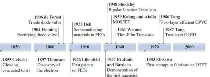
Figure 1.17: John Bardeen(with spectacles), William Shockley and WalterBrattain at Bell Labs, 1948...30
Figure 1.18: History of transistors...31
Figure 1.19: Moore’s law...32
Figure 1.20: Shows different configuration of FETs...33
Figure 1.21: a) showing the positions of HOMOs and LUMOs with respect to the Fermi levels of the source and drain and their change...35
Figure 1.22: a) Carrier concentration profile of TFT in different regimes et...37
Figure 1.23: showing ID – VD curves for TFTs at different values of VG...39
Figure 1.24: showing ID –VG curves at a constant value of VD ...40
Figure 1.25: Showing first SWNT- FET device...42
Figure 1.26: Device architecture of the first Si based FETs...42
Figure 1.27: the output characteristics of the first CNT FETs developed by Dekker’s group...43
Figure 1.28: Device architecture for inkjet printed transistors work by Sadiral e...45
Figure 1.29: Mobility plots extracted from devices made by increasing the number of printed passes work by Sadir et al...45
Figure 2.1: Chemical structure of Polyethylene Naphthalate...46
Figure 2.2: Chemical structure of Poly ethylene Terephthalate...47
Figure 2.3: Chemical structure of PEDOT: PSS...47
Figure 2.4: Chemical structure of PMMA...48
viii
Figure 2.6: Absorption spectrums of HiPCO: P3DDTin toluene
and oDCB after the 1st centrifugation...51
Figure 2.7: View of Dimatix Printer...52
Figure 2.8: A Dimatix Matrix Materials Cartridge...53
Figure 2.9: Photo of Dimatix Printer...54
Figure 2.10: TQC bar coater...54
Figure 2.11: The coating rods with different wire spacing diameters...55
Figure 2.12: Photo view of TQC coater...56
Figure 2.13: Schematic representation of Stylus profilometer...56
Figure 2.14: Photo view of the place where the sample is place profilometer...58
Figure 2.15: Photo view of the profilometer setup...58
Figure 2.16: Photo view of the Stylus prober...59
Figure 2.17: Prober in the Glove Box...60
Figure 2.18: Annealing of samples...61
Figure 2.19: Working of Scanning Electron Microscope...62
Figure 2.20: Architecture of the device...65
Figure 3.1: Mobility curves of spin coated N2200 and CNTs device...68
Figure 3.2 Mobility curve showing sonication effect...69
Figure 3.3: Plot showing the difference in the performances of the devices fabricated with spin and bar coating of the dielectrics...71
Figure 3.4: Shows transfer curves of the best fully printed device...72
Figure 3.5: Shows output curves of the best fully printed device...73
Figure 3.6: Mobility curve of the best working printed device...74
Figure 3.7: shows the SEM image of CNT solution with o-Xylene after bar coating...75
Figure 3.8: The transfer characteristic curve of device plotted with 10 µm pitch bar and 20 µm coater. ...76
Figure 3.9: The mobility curves of the device with the semi-conductor formulation with CNTs solution and o-Xylene...77
Figure 3.10: Shows the transfer characteristics of a device fabricated with dielectric PMMA prepared at concentration 90 mg/ml and 80mg/ml...78
1
INTRODUCTION
Printing has very ancient origins, and since the invention of the printing press by Gutenberg in the 15th century, it has evolved to replicate information in mass volumes at low cost, up to the contemporary roll-to-roll industrial graphical arts technology. The recent development of solution-processable functional materials with electronic properties, including semiconductors, conductors and dielectrics that can be formulated in the form of inks has allowed to develop what is called “Printed Electronics”. The latter is a branch of electronics where graphical arts printing technology has been and is continuously being adapted to the needs of functional inks and electronic applications, to deploy electronic and sensing functionalities, at low temperature and high-throughput, typically on plastic or paper substrates, targeting large-area and flexible applications. It is not a competitor of established silicon technology, but it rather aims at turning passive surfaces of even low cost objects into active components, integrating micro- and opto-electronic functionalities. Examples are disposable point-of-care applications, low cost smart tags, smart packaging, flexible and/or rollable displays, wearables, local body area networks.
Among printable materials, both polymer conductors, such as PEDOT:PSS (conductivity up to 1000 S/cm) and highly conductive metallic inks, such as silver nanoparticles or metal complexes based inks (conductivity up to 104 S/cm) are largely available. Printable dielectrics are as well very well covered, comprising a lot of commodity polymers. Different possibilities have been developed for what concerns semiconducting inks, among which organic conjugated materials have clearly represented one of the most promising options for large-area printed electronics, because of their chemical tunability, which simplifies inks formulations, their low temperature processing. their robust mechanical properties and electronic and optoelectronic properties which have steadily improved over the last few decades. However semiconducting polymers still show strong limitations, which are reflected in relatively poor electronic performances of fully printed electronic devices. As an example, despite the steady improvement of recent years, polymer field-effect transistors (FETs), which can be considered the fundamental building blocks of
2
polymer electronic circuits, show a carrier mobility which for the best semiconductors is in the range of 1 to 10 cm2/Vs, and typically lower than 1 cm2/Vs in case of fully printed FETs. Another strong limitation is represented by the Schottky barriers developing at polymer semiconductor and electrodes interface, leading to strong contact resistance effects, posing a severe constraint on the device downscaling. The previous limitations, combined with the typical coarse resolution of state-of-the-art printing technologies, typically lead to poor switching performances of fully printed FETs, therefore strongly limiting the overall expected speed of a printed polymer circuits, and as a consequence, limiting also their possible applications. It is therefore desirable to find alternative solution-processable semiconductors, which ideally maintain the ease of formulation and printability of polymers, but at the same time offer improved electronic performances.
This thesis focused on the assessment of semiconducting single-walled carbon nanotubes (swCNTs) formulations as alternative to polymer semiconductors for the fabrication of fully printed field-effect transistors on plastic substrates. While CNTs offer in principle much better electronic performances with respect to polymers, especially in terms of charge mobility, economically viable methodologies to produce them lead to strongly entangled mats of conducting and semi-conducting nanotubes. Moreover, their dispersion in suitable solvents to formulate stable, printable inks is still a challenge. In this work we focused on the use of swCNTs well-sorted and dispersed thanks to a polymer wrapping approach, where a semiconducting polymer capable of selectively wrapping specific chiralities, and therefore swCNTs with specific bandgaps, can be used both as a sorting agent and a dispersant. The formulations adopted have been provided by the group of Prof. M.A. Loi at the University of Groningen, an international leader in this approach which has first proven the possibility of achieving FETs with solution-processed swCNTs networks with high mobility, in excess of 10 cm2/Vs. The specific goal of the present work was to study the possibility of depositing by means of bar-coating, a very simple and scalable technology compatible with roll-to-roll printing, carbon nanotubes networks from formulations of swCNTs wrapped by Poly(3-dodecylthiophene-2,5-diyl) P3DDT , which is a conductive polymer. More specifically, the study has first aimed at fabricating and validating a reference fully printed FET architecture on PEN
3
substrate based on a well-known model semiconducting polymer, namely Naphthalene diimide(N2200) . Such polymer FET, that was realized by inkjet printing PEDOT:PSS source/drain and gate contacts, and comprised a bar-coated (PMMA) Poly Methyl methacralate,dielectric and a bar coated N2200 semiconductor achieved a field-effect mobility of 0.62 cm2V-1s-1 and served as a benchmark for swCNTs based devices. Subsequently, deposition of swCNTs networks both by spin-coating and bar-coating was optimized especially in terms of coverage of the substrate and integrated into FET devices to assess their performances. Thanks to the achievement of controlled deposition of swCNTs networks by bar-coating on PEN, functional fully printed FETs with hole mobility reaching 1.90 cm2/Vs were finally achieved, a result which represents a first promising step towards high performance, fully printed CNTs based flexible circuits.
This work was performed in collaboration with Istituto Italiano di Tecnologia (IIT), and the experiments were conducted in the laboratories of the “Printed and Molecular Electronics” group at the Center for Nano Science and Technology of IIT in Milan. All swCNTs formulations were provided by the group of Prof. M.A. Loi at the University of Groningen, Netherlands.
The thesis is organized as follows:
Chapter 1 provides a general introduction to printed electronics- polymers, inkjet
printing, carbon nanotubes and filed effect transistors.
Chapter 2 relates to experimental part that is the materials, equipments and the
fabrication methods\
Chapter 3 provides theresults and analysis of the experiments conducted during the
4
Chapter 1
Background Knowledge
1.1 Introduction to printed electronics
Printed electronics is a subject of electronics which deals with solution printing of thin films on various substrates. Electrically functional electronic or optical inks are deposited on the substrate creating active and passive components such as thin film transistors, resistors, capacitors and coils. Here the inks can be composed of different carbon based compounds and these can be deposited by solution based techniques. The main feature of printed electronics is that, it gives us a possibility to print many micro-structured layers one above another in a much simpler and cost effective manner. This gives a wide opportunity to implement new and improved functionalities to the device. The resolution of printing is very high (in µm or nm) with precision.
Printing technologies divide between sheet-based and roll-to-roll-based approaches. Sheet-based inkjet and screen printing are best for low-volume, high-precision work. Gravure, offset and flexographic printing are more common for high-volume production, such as solar cells, reaching 10,000 square meters per hour (m²/h).[1][2] While offset and flexographic printing are mainly used for inorganic[3][4] and organic[5][6] conductors (the latter also for dielectrics),[7] gravure printing is especially suitable for quality-sensitive layers like organic semiconductors and semiconductor/dielectric-interfaces in transistors, due to high layer quality.[7] If high resolution is needed, gravure is also suitable for inorganic [8]
and organic [9] conductors. Organic field-effect transistors and integrated circuits can be prepared completely by means of mass-printing methods.[7]
Both organic and inorganic ink materials can be used for the printing methods provided with proper control in their viscosity, surface tension and solid content. Solubility, wetting, adhesion as well as post treatment conditions after deposition play a very vital role, since they have the ability to change the morphology of the layers. With respect to the conventional electronic methodologies, printed electronics provides an opportunity to modify the mechanical flexibility and functionality by chemical adjustment.
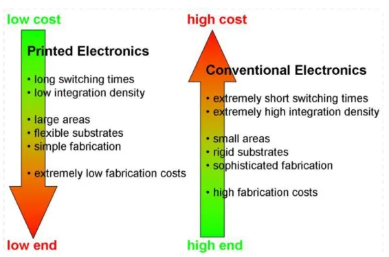
5
Obviously, the performance is not expected to be as great as that of the conventional electronics, since they are solution processed and the charge carrier mobility is lower than conventional method.
Figure 1.1 A brief summary between printed and conventional electronics
Conductive polymers are the materials which can be used for solution processed applications. Other alternative materials with high performance are also researched.
1.1.1 Organic Semi Conductors
Organic semiconductors are the carbon based conjugated systems having delocalized π bonds. Carbon have an electron configuration of 1s2 2s2 2p2, in total of six electrons, with four valence electrons available for pairing. Through the linear combination of the 2s and 2p atomic orbitals, the atom can form hybridized sp, sp2 or sp3 orbitals, with its four valence electrons that can participate to the formation of up to four bonds. While the electrons in the hybridized orbitals can form strong covalent σ-bonds with other atoms, defining the organic compound backbone, those of the 2p orbitals (not involved in the hybridization) form the weaker
π-6
bonds (fig.1.8). This type of bond allows the delocalization of the free electrons over the carbon atomic plane, attributing semiconducting properties to the system. Two or more atoms connected by σ-bond and π-bond constitute a conjugated molecule.[10]
Figure 1.2: Sketch of the double bond between two sp2 hybridized carbon atom
The repetition of these conjugated sub-units (monomers) results into the polymers. With the increase in the monomers the conjugation increases, facilitating the electronic delocalization. Delocalization is eased by reduction in the energy gap between the HOMO (highest occupied molecular orbitals) and LUMO (least occupied molecular orbitals) levels.
To briefly, understand the charge transport in the organic semiconductors, it is important to know the concept of polarons. Since, contrary to the metals, the electrons are localized in the semi-conductor results into local deformation of the molecule. This charge structure interaction can be described as a strong electron-phonon coupling and therefore for charge transport this electron-phonon and charge must move coordinately. This quasiparticle couple is called polaron. By applying an external field, the polaron can travel across the system carrying the local deformation of the lattice. Thus, the polaron can be positive or negative with spin of (+,-) ½ and can be considered as a defect due to the vacancy of an electron. Furthermore, in the case of a second doping stage, if we remove a second electron, the formation of a
bipolaron occurs. This new spineless now particle, can be again positive or negative but
stable bipolarons are known to exist in a few materials, including polyacetylene and a number of oxides. [11]
7
Figure 1.3: Band structure containing a positive polaron and a positive bi polaron
The charge transport within a molecular solid has two main components; an intra-molecular, or rather the motion of the polaron along the chain and the inter-molecular that regards the jump of the charges between the molecules composing the molecular solid.
The first is a coherent event which takes place within extended molecular states. On
Figure 1.4: Charge transport; 1-2; a backbone charge transfer -intra-molecular. 2-3, inter-chain transfer though hopping
8
the other hand, the inter-chain transfer is the most spread charge transport mechanism,plays a crucial role in the charge transport [12] and is governed by the presence of weak inter-chain reaction and by the degree of disorder in the organic system. Some of the semi-conducting polymeric materials are N2200, PEDOT: PSS, P3HT, P3DDT.
1.1.2 Carbon Nanotubes as semi conductors
Carbon nanotubes as discussed earlier in the section 1.1, provides an alternative to the use conventional polymers as semiconductors. They having outstanding electrical and mechanical properties, along with processibility in solution deposition methods makes them suitable candidate as semi-conductors. Although it has to be mentioned that various techniques such as gel chromatography, polymer wrapping etc. needs to be employed in order to separate tthe semi-conducting carbon nanotubes from the metallic ones with very high purity for better performances in the devices.
Carbon nanotube based polymer solution have been successfully used in coating methods like spin coating[13,14], spray coating[15], self assembly coating[16], dip coating[17], rod coating[18] to printing techniques such as screen printing[19] , inkjet printing [20]aerosol printing [21–23] , transfer printing [24], and contact printing [25] techniques have eliminated the need of using a high-vacuum environment and multistage patterning process, thus paving the way for scalable manufacturing of large-area, low-cost, and flexible electronics.
1.1.3 Inkjet Printing
Inkjet printing offers unique advantages over other methods of printing. It requires absolutely no prefabrication of templates, allowing for a rapid printing process at low cost. Additionally, due to its precise method of patterning, post-printing steps are not necessary. Furthermore, multiple materials can be deposited simultaneously with the use of multiple ink cartridges, and the amount of deposited material can be controlled with great precision. Finally, due to the nature of inkjet printing technology, multiple layers can be printed on top of one another with great ease.
9
1.1.3.1 Classification of Inkjet Printers
Inkjet printers can be classified based on its principle of printing technology into two categories- Continuous and Drop on Demand.
Continuous
Continuous inkjet printing supplies a continuous stream of ink droplets. The principle is that these droplets are charged upon leaving the nozzle and are then deflected by voltage plates, where the applied voltage determines whether the droplet will be deposited onto the substrate or recycled through the gutter. Therefore, even though when the printer is not actually printing anything onto a substrate, a stream of droplets is still being ejected from the nozzle and recycled through the gutter.
Drop on Demand
As the name suggests, a drop-on-demand inkjet printer ejects a droplet of ink only when it is told to do so. Therefore, when the printer is not actually printing anything onto a substrate, there are no droplets being ejected from the nozzle. Drop-on-demand inkjet printers can be further split into two categories, namely thermal and piezoelectric.
Thermal inkjet printers
Thermal inkjet printers, at times referred to bubble jet printers, contain a thin film resistor in the nozzle. In order to eject a droplet, this thin film resistor is heated by passing current through it. This causes the ink in the nozzle to vaporize, creating a bubble and a large increase in pressure, which forces ink droplets out of the nozzle. Hewlett-Packard, Canon, and Lexmark employ this type of drop-on demand inkjet printer.
Piezoelectric inkjet printers
They contain a piezoelectric transducer in the nozzle. When voltage is applied to the piezoelectric transducer, it deforms and causes an increase in pressure, which forces
10
ink droplets out of the nozzle. In terms of consumer printers, Epson employs this type of drop-on-demand inkjet printer. The Fujifilm Dimatix printer, which is specialized commercial inkjet employ the piezoelectric drop-on-demand technology as well. Dimatix printer 2830 is used in this work, because of control over drop volume and spacing and therefore better resolution can be obtained.
Based on the usage, the printers be classified into consumer and commercial printers. Consumer based printers
Consumer inkjet printers are quite cheap and offer familiarity, so there is no need to learn new software or hardware. Nevertheless, these printers are made to print a specific type of ink, so developing useable ink can be a bit more difficult. The new ink must match the original ink in all aspects. Furthermore, in the instance where a new ink clogs the nozzle, some consumer inkjet printers are easier to clean than others. In general, each Hewlett-Packard printer cartridge has its own nozzle, allowing the user to easily remove the cartridge and clean it. On the other hand, the nozzle for Epson printer cartridges is built into the printer itself and cannot be easily removed for cleaning. The most prominent disadvantage for consumer inkjet printers is their overall lack of control. In particular, the drop volume and spacing cannot be adjusted, and the resolution is relatively low.
Commercial based printers
Commercial printers are used since they have a great deal of control over drop volume and spacing, and they provide better resolution. Though expensive, these printers, like the Fujifilm Dimatix are specifically made for printing various types of materials.
1.1.4 Bar coating
Bar coating is used in order to print the carbon nanotube semi conducting active layer and the dielectric. Bar coating set up consists of the substrate placing plate. A bar is moved at a certain set velocity over this, after placing the substrate. Depending on the type of bar configurations and the velocity the thickness of the layer is determined.
11
Different types of bar
12
Wire wound rods
The original “Mayer” rod. Popularized by Charles Mayer in the 1920's and still the most popular. Wire wound rods can be stripped and rewound to save cost and reduce waste. There are no minimums and no setup charges for wire wound rods.
Formed rods
A formed (threaded, grooved, etc.) rod is roll formed from a solid steel bar and closely resembles a wire wound rod. The size of the groove determines the coating thickness the same way the cavity between wire winding does. However, the radius in the groove of a formed rod is less likely to clog and cleans up easier than its wire wound equivalent.
Smooth rods
Commonly used to smooth previously metered coatings to paper, paperboard and plastic films. The coating thickness is governed by pressure (against a backer roll) or web tension. RDS smooth rods can be ground to meet any surface finish requirement and hard chrome plating can extend rod life significantly.
Gapped rods
For higher viscosity coatings, gapped rods reduce clogging and eliminate lines. By winding a smaller wire with spacing (see image) the cavity created is wide and shallow allowing heavy coatings to flow better. A smaller wire creates a smaller interruption in the coating flow enabling the coating to wet out more completely. While a gapped rod is less durable than a double wound rod, it is also less expensive.
Double wound rods
For higher viscosity coatings, double wound rods reduce clogging and eliminate lines. By winding a smaller wire on top of a larger one (see image) the cavity created is wide and shallow allowing heavy coatings to flow better. A smaller top wire creates a smaller interruption in the coating flow enabling the coating to wet out more completely. While a double wound rod is more expensive than a gapped rod, it is also more durable.
13
1.2 Carbon Nanotubes
The history of carbon nanotubes goes back farther than most people think.
In fact, a US patent was given to two British men in 1889, on the production of carbon nanotubes utilizing marsh gas, otherwise known as methane. The method employed is essentially the same as used today. The patent describes the production of “hair-like
carbon filaments” for electrical lighting. This patent also described about some of the
unique electrical and mechanical properties, “Carbon filament may be bent and twisted into various shapes and will spring back to their original form on being released.”[26]
In 1960’s a group at National Carbon Company in Parma, Ohio and later
in the 1970’s at and the University of Canterbury in Christchurch, New Zealand, helped to characterize the carbon nanotubes.
Later in 1983, a company called Hyperion Catalysis perfected ways to produce nanotubes and began incorporating them into fuel line for cars. The nanotube’s high conductivity would dissipate any electrical charge that could potential build up and spark. Today, 60 percent of the cars on the road use Hyperion’s nanotube incorporated fuel lines. Hyperion’s nanotubes are also incorporated into plastic wing panels. This allows the plastic on the wing to be grounded and then sprayed with paint droplets that are charged up to 20,000 volts. The drops are attracted to the wing and stick, thus reducing the wasted paint that would normally mist away in the air.
The real research and work with carbon nanotubes began in 1991, when Sumino Limijima and his colleagues created some nanotubes at the research laboratory of the electronics multinational NEC in Tsukulba, Japan[27]. Here they used, high-resolution transmission electron microscopy to observe carbon nanotubes, that the field really started to take off.
Researchers at the Institute of Chemical Physics in Moscow independently discovered carbon nanotubes and nanotube bundles at about the same time, but these generally had a much smaller length-to-diameter ratio. The shape of these nanotubes led the
14 Russian researchers to call them "barrelenes“.
1.2.1 Structure of Carbon Nanotubes
Carbon nanotubes are rolled up graphene layers, which are generally 0.2- 5 µm long having diameters up to 1-2 nm. The honey comb sheets of carbon are rolled up into cylinder. Multiwall carbon nanotubes and single wall nanotubes are the two different types of nanotubes depending upon the rolling.
Figure 1.6: Types of Carbon nanotubes
The possible ways of rolling of the graphene layer gives different CNTs -Zig Zag, chiral and arm chair. The characteristics of these CNTs are that they are metallic or semi-conducting in nature depending upon their rolling up.
is a chiral vector which is related to the diameter of the tube.
A chiral vector is defined as in terms of and , and is a linear combination.
and are unit vectors which define the graphene lattice and θ is the angle between one of the two unit vectors, either or and the chiral vector .
15
Figure 1.7: Building of CNTs from graphene sheets, the primitive vectors and an example of chiral vector and chiral angle.
Figure 1.8: Bravais Lattice of graphene
Based on interpreted with the θ angle, which is the angle between the chiral vector, carbon nanotubes can be classified into some specific structures.
Chiral : 0⁰<θ<30⁰ Zig-Zag : θ = 0⁰ or 60⁰ Arm chair : θ = 30⁰
16
Figure 1.9: Different types of CNT: depending on the rolling.
From the study of band structure, we get to the conclusion that the zig-zag and the chiral have 1/3rd metallic and 2/3rd semi conducting CNTs and for arm chair confurigation all the CNTs are metallic in nature.
Hence in the device we can use only zig zag and chiral ones, as they can be used as semi-conductors. Very high purity of semi-conducting carbon nanotubes must be used for the active channel. This is important since, it affects the performance of carbon nanotube transistors affecting the current ON/OFF ratio.
Sorting of carbon nanotubes is required. Many techniques are used in order to sort the semi-conductor and the metallic tubes.
1.2.2 Electronic properties of SWCNTs
Since, the SWNTs are rolled up graphene layers; hence their electronic properties of SWNTs derive from the electronic configuration of graphene, in which the bonding π orbitals form valence states and the anti-bonding π* orbitals form conduction states.
17
Figure 1.10: shows the band structure in the extended first Brillouin zone of graphene
Figure 1.11: Energy diagram and Density of States(DOS) a)of m-SWNTs and b)s-SWNTs . The shapes peaks are the van Hove singularities of SWNTs
The unique electronic properties of SWNTs originate from the quantum confinement of the electrons normal to the nanotube rolling axis.
The periodic boundary conditions around the nanotube circumference require that the component of the momentum ( ) along the circumference is quantized ( , where j is a non-zero integer).[28] This quantization leads to the formation of a set of discrete sub-bands for each nanotube as described by the red parallel lines in Figure 1.11. The crossing of these lines with the band structure of graphene determines the electronic structure of the nanotube. If the lines pass through the Fermi point (K or K’), the nanotube is a metal (m-SWNT); otherwise the nanotube is a semiconductor (s-SWNT).
18
The nature of the tube in terms of metallic or semiconducting behaviour is also
related to the values of the indices (n, m). When |n-m| = 3q (where q is an integer), the nanotubes are metallic or semi-metallic. In any other case, they are semiconducting. Theoretically, in an as-synthesized crude mixture of SWNTs there are approximately one-third metallic/semi-metallic SWNTs and two-third semiconducting SWNTs available.[29]
The transition energy (band-gap) of semiconducting nanotubes Eg can be described by using a simple tight-binding model, given by the equation:
Where,
is electron Fermi velocity
γ is the nearest neighbour interaction energy is the nearest neighbour C-C distance and
is the nanotube diameter.[30]
Their electronic states are organized in discrete bands, with a one-dimensional density of electronic (DOS) states known as van Hove singularities. Two examples of energy diagram and DOS of m-SWNT and s-SWNT are presented in Figure 1.11a and b, respectively. No real band gap is observed in the m-SWNT system.
1.2.3 Charge Transport in CNTs
Due to the confinement along the circumferential direction, SWCNTs are in the class of the quantum mechanical systems. Thus the transport properties can be described considering the model for 1D nanowires, with the lateral dimensions W,
H much smaller than the length L (W, H « L).[31] [32] To understand the different transport regimes, we define the important length scales that are involved in the electron motion:
λF = 2π/KF , the Fermi wavelength, which is the wavelength of the electrons at
the Fermi level. It is related to the Fermi energy of the free electron gas
19
This coincides with the length for which the quantum effects are relevant, i.e. the quantization of the bands in SWCNTs due to the lateral confinement.
λcoh, the coherence length, which indicates the mean distance that the electron can travel without losing its phase due to phonon-electron, electron-electron or defects scattering.
λel, the elastic mean free path which represents the travelling length of the electron before it undergoes an elastic scattering event. The elastic scattering leaves the electron phase unchanged, differently from the inelastic scattering events, but changes the electron momentum.
λloc, the localization length which indicates the average spatial extent of the states in the system under study. In a infinite 3D pure crystal λloc = ∞ and the electron is completely delocalized. In the presence of a certain
degree of disorder, λloc and the electron can be weakly or strongly localized.
In nanowires with lateral dimensions W, H <= λFand length L » λF, the quantum
lateral confinement produces the discrete one dimensional sub-bands. Consequently the conduction is quantized and occurs though the 1D sub-bands that are named conduction channels. In this situation the transport along the wire axis depends on the characteristics length scales and could be diffusive, in which the L » λeland the resistance grows linearly (incoherent transport) or exponentially
(coherent transport), or ballistic, in which no scattering events are present and the resistance is determined by the number of conduction channel and it is independent of the length. In this last regime, to estimate the conductance in a single channel, we can use the Landauer theory considering the conductor connected with two electrodes. The electron waves that approach the conductor from the electrodes are partially transmitted and reflected through the electrodes. For a given energy, several modes propagate inside the electrodes. Thus we can
20 define the Landauer conductance as:
G= GοT(E) with
where T(E) is the sum of the transmission probability over all the modes, that at zero temperature is limited to the mode at EF
Go is called conductance quantum
In a situation of transparent electrical contacts, in which no reflection occurs, and highly order in the system (T = 1), the conductance formula becomes:
G = GoN with
where N is the number of transmitted modes and Go represents the conductance of the single mode. m-SWCNTs, i.e. armchair[10, 10], possesses two sub-bands which cross the Fermi level, resulting in two conducting channels.
If the scattering length within the nanotube is much longer than the length of probed nanotube and the contacts are transparent, the conductivity of the nanotube has the ideal value G = 2Go.[33] However, in the real experiment, the environment (substrate), the presence of centers of scattering such as defects, impurities and distortion on the structure and the choice of the contacts material negatively affects the theoretical conductance.
21
1.2.4 Transport in CNT Networks
To understand the transport in carbon nanotube networks and also the various factors involved in the carbon nanotube charge transport various research works have been done and theories established on various factors which may be affecting the transport phenomena in the carbon nanotube networks. It is quite obvious to understand that the carbon nanotubes’ transport processes would be different in the case charge transport in single carbon nanotubes and when in networks. The proximity of the CNTs even modifies the intra-nanotube transfer. This is affected through bending and distortion of the lattice as well as Wan der Waal’s inter-nantube interaction. These two effects results into energetic barrier that hinders the charge transport and consequently decreases the conductivity.
The observed the side walls of nanotube are same as the graphene sheets in the graphite is around 3.5⁰ A. When the simulations in the model with length higher than 3⁰A done, it was demonstrated that the interaction between the orbitals of the two nanotubes decreases and the quantum conductance presents discrete resonant peaks.[34] This makes the hopping phenomena responsible for the charge transport. Thus, charge can hop from one tube to another tube through resonant tunneling and the conductivity of the network depends on the intertube tunneling efficiency. With this principle, the phenomena why the ordered networks have higher conductivity can be demonstrated. This is because, in the ordered networks, the contact surface between the nanotubes, is higher than the randomly distributed networks, hence increasing the probability of the tunneling event and the conductivity overall.
In the device, practically, the other aspects like different deposition methods, synthesis, presence of different chiralities and introduction of impurities or other chemical species as in the case of functionalized nanotubes play a very important role.[35]
The different methodologies used for synthesis of Carbon nanotubes lead to metallic and semiconducting species, with wide range of chirality that are randomly interfaced in a network.
22
According to the perturbation theory, the resonant tunneling events between two states happen at the Fermi-point of two nanotubes only if the conservation of the momentum and energy is generated. Different chiralities posses’ different Fermi momenta, hence, poor tunneling, thus are lowering the values of conductivity.
Another important factor which affects the transport phenomena of the carbon nanotubes is the density of the networks or the number of the carbon nanotubes involved in the bulk film. Modeling the nanotubes, as conducting sticks and implying the percolation theory, it predicts that
with
Where
1.2.5 Contacts to Nanotubes: Schottky Barriers
Two types of barriers can form at the metal/tube interface and increase the contact resistance beyond the ideal h/4e2 value. The first is a barrier created by an imperfect interface between the contact metal and the nanotube. Its resistance is a function of the cleanliness of the interface and the overlap of the metal–nanotube electronic states. Au and Pd have proven to make the best contacts to nanotubes, with near-perfect transmission frequently obtained [36].
More fundamental is the Schottky barrier that can form at the interface of a metal and a semiconducting nanotube. The properties of the Schottky barrier will depend on the band alignment at the interface (Fig. 1.12a). In the absence of interface states believed to be a good approximation for the metal/tube interface [37] , the heights of the Schottky barriers for hole and electron injection are given by the work function of the metal contacts, φM, the work function of the nanotube, φNT, and its energy gap, Eg.
23
When the Fermi level of the metal lies at the midgap of the nanotube (Fig. 1.12b) there will be a Schottky barrier for both n and p carrier injection, whereas when it aligns with the hole band (Fig. 1.12c) there would be no barrier to hole injection but a large barrier to electron injection.
a) b) c)
Figure 1.12 a) A schematic of the non aligned metal and nanotube energy levels depicting the relation between the Schottky-barrier heights for hole (/electron) injection, φpSB (φn
SB) and the workfunction of the metal, φM, the work function of the tube, φNT, and its energy gap Eg.When both are put in contact, band bending at the interface occurs to compensate for the work-function difference. (b) The case for contacts with the work function at
the nanotube midgap. (c) p-type contacts.
From different experiments, it has been made clear that the contact properties very sensitive to the ambient environment and device history. It was also noted [36] that a high work function by itself is not sufficient to assure ohmic contacts. For example, Pt
24
has a larger work function than Pd but forms more resistive contacts, probably due to additional tunneling barriers formed as a result of poor wetting of the tube by the contact metal.
Since the energy gap grows with decreasing diameter ( it is clear from the above equation that for every metal there exists a critical nanotube diameter below which a Schottky barrier with finite height will form and the height of this barrier will increase with decreasing diameter.
The assessments in the past have provided a consistent picture of contact properties of semiconducting nanotubes, although a major challenge remains to make good ohmic contacts to tubes with diameters 1.5 nm and smaller. Surprisingly, even small-bandgap/metallic tubes show significant barriers in this range [38] . The origin of this behaviour is still not completely understood.
1.2.6 Synthesis and sorting of Carbon Nanotubes
By the different synthesis methods, the diameter of the SWNTs can be modulated; consequently the band gaps and their conducting and metallic nature. HiPCo method, High pressure carbon monoxide disproportionation process which uses of flowing CO gas with Fe(CO)5 as catalyst produces SWNTs with diameter 0.7- 1.2 nm.
Another method the CoMoCAT method uses molybdenum and cobalt as catalysts results into SWNTs with 0.8 nm, where as with the arc discharge method tubes of diameter around 1.5 nm. This method uses high current to carbon rods. Another technique called the laser ablation method too produces CNTs of diameter around 1.5 nm, using vaporization of carbon atoms from graphite target in an inert atmosphere by a high power laser. It must be noted that just after their synthesis, SWCNTs have a natural tendency to form bundles because of the Van der Waals’s forces between their walls.
25
The methods that are used to separate metallic and semi conducting SWNTs are based on the functionalization of the SWNTs walls. These processes can be divided into two categories: covalent and non covalent functionalization.
Covalent functionalization is a technique which is used from 1998 and in order to
increase the solubility of SWNTs. This discrimination is based on the electronic properties. This method affects the band gap converting the m-carbon nanotubes into semi conducting ones. The disadvantage of this method is that it affects the charge transport by introducing scattering sites for charge carriers.
The non covalent functionalization method which is widely used is using Sodium dodecyl sulphate (SDS), sodium cholate, sodium dodecylbenzene sulphonate (SDBS), and many other bile salts to disperse SWNTs in aqueous solution. The principle is based on the hydrophobic group (tail) in contact with the nanotube and hydrophilic group (head) in contact with the water. There is no efficient separation by these surfactant-dispersed SWNTs, due to the interactive nature of the CNTs.
Density gradient ultracentrifugation (DGU) (see Figure 1.13a) is the first method which showed the separation between semiconducting nanotubes and the metallic ones. [39] This method used a mixture of two surfactants in different ratios. Next step was ultracentrifugation in a density gradient medium, hence, the carbon nanotubes (CNTs) were sorted based on the density difference and therefore by diameter and band gap . It was quite interesting that this resulted in a multi-layer coloured solution, where different colours corresponded to tubes of different band gaps. Repetition centrifugation processes resulted in to SWNT fractions having a narrow distribution of nanotube diameters. This is a very effective technique applied for commercial purposes, separating both SWNTs produced Arc Discharge method with a high 99% semiconducting and 98% metallic purity.
Gel chromatography is another method which is (Figure 1.13b) based on the specific adsorption of SWNTs in an allyl dextran-based gel. The interaction of this gel media is differently with s-SWNT and m-SWNT, such as van der Waals forces.[40] Different interaction of the nanotubes with different curvature will have been given by different surfactant coverage. Hence, by performing multicolumn gel chromatography, and
26
In different columns, by successively injecting SDS surfactant to the vertically stacked column, SWNTs with different diameter and chiralities can be obtained . Using this agarose gel technique, it is possible to obtain large-scale separation of SWNT, up to the scale of liters.This technique allows to obtain separation of SWNTs in large scale up to litres.
Figure 1.13: (a) Density gradient ultracentrifugation (DGU) (b) multicolumn gel chromatography, and (c) Agarose gel technique
Another technique obtained by Krupke et al. to discriminate metallic and semiconducting SWNTs from a raw mixture using dielectrophoresis.[41] In this method, an electric field gradient generated by a microelectrode array and placed on a SDS-based SWNT dispersion. Hence, in this way the semiconducting SWNTs remain in a stationary position, while the metallic tubes migrate towards the electrodes due to their greater dipole moment and is collected [42]. For large scale separation of s-SWNTs, agarose gel electrophoresis is used.
27
1.2.7 Polymer wrapping of Carbon Nanotubes
Polymer wrapping method uses molecules to wrap and select s-SWNTs. This method was adopted from the interesting feature of DNAs is that their nucleobases have π stacking interaction with the surface of the s-SWNTs, resulting in helical wrapping at the surface of the tubes.
Figure 1.14: Showing the Carbon Nanotube wrapping with polymers
The principle includes, that the conjugated back bone wraps up around the nanotube wall, while the polymer chains which are hairy wraps the SWNTs wall with the Wan der Waal’s interaction. Several simulations performed by Gao et al. give an indication that the alkyl tails of neighbouring polymer chains zip and align around the nanotubes due to the Wan der Waal’s interaction. Polyfluorene derivatives have an affinity towards different chiralities and diameters of SWNTs. Literature shows that these polymers in particular have selectivity towards CNTs produced by the HiPCo method with larger diameter. Poly(9,9 didodecylfluorene-2,7-diyl-altanthracene-1,5-diyl) (PF12-A) shows selectivity to nanotubes with larger diameter, and it is claimed that
28
this large diameter selectivity is due to the anthracene unit. In contrast to other fluorene copolymers, poly(9,9-dioctylfluorenyl-2,7-diyl and bipyridine) (PFO-BPy) can extract almost single chirality small diameter nanotubes
(97% of (6,5)-SWNTs) using p-xylene as solvent. This result opened the opportunity for extracting single chirality s-SWNTs using polymer wrapping.
Figure 1.15: wrapping orientation with different polymers
It has been reported by Bao et al demonstrating that poly thiopenes with long alkyl chains have a good efficiency to disperse and separate carbon nanotubes. The best polythiophene derivative they reported is regioregular poly(3-dodecylthiophene) (rr-P3DDT).
29
Figure 1.16: Different polymers used for separation of semi conductive CNTs from metallic ones
30
1.3 Transistors and Field Effect Transistors
The history of transistors goes back to the year 1947, when John Bardeen (1908- 1991), William B. Shockley (1910-1989) and Walter H. Brattain (1902-1987) invented the first transistor made up semi conductor material which was able to do both- amplify an electrical signal and secondly, allow flow of current. This was developed in the Bell labs when they were trying to find a replacement of the old and bulky vacuum tubes. Before this, the vacuum tubes were used in the telephone technology, amplifying current. Since they are not so reliable and excessive power was consumed.
Figure 1.17: John Bardeen(with spectacles), William Shockley (using the microscope) and Walter Brattain (standing behind) at Bell Labs, 1948 [43].
After the invention of germanium transistor the three terminal device known as the
“point contact” device (in the middle of last century), inorganic semiconductors have
31
Figure 1.18: History of transistors
In 1960, Kahng and Atalla [44] fabricated the first silicon-based metal-oxide- semiconductor transistor. This was ground breaking and since then technology and processing of transistors based on silicon has seen an upsurge.
In these recent years, increasing interest has been focused on Organic Electronics, since there an ease of fabrication of these transistors, along with the cost effectiveness. A research field focused on this has been working continuously to improve the performance of the transistors. The current ON/OFF ratio, mobility, working at low voltages hence lower power consumption are the main parameters which are mainly optimized on. This would lead to a low cost, large area plastic electronics employing transistors and diodes based on organic semiconductors. For the advances in the field of electronics, realization of Moore’s law is necessary so miniaturization of transistors play a very vital role.
The Moore’s law as observed in 1965, states that the number of transistors in a dense integrated circuit doubles approximately every two years. The observation is named after Gordon Moore, the co-founder of Fairchild Semiconductor and Intel, whose 1965 paper described a doubling every year in the number of components per integrated circuit,[45] and projected this rate of growth would continue for at least another decade.[46]
32
Figure 1.19: Moore’s law
1.3.1 Field Effect Transistors
The first demonstration of field effect in a carbon based material was observed in an organic molecule, phtalocyanine, in 1964[47], but only later, in the 1987, the first organic polythiophene-based FET was realized by Koezuka[48]. This development consequently buoyed up intense study of carbon based compounds, leading to the synthesis of organic semiconductors with increasingly performance. However, over the last twenty years, the discovery of new carbon allotropes, such as graphene and carbon nanotubes, and their outstanding electrical properties gave a huge impetus to the fabrication of FETs with the highest performance ever.
1.3.2 Geometry of Field Effect Transistors
Field effect transistors, also known as thin film transistors, when their fabrication is done by deposition of thin films, consists of three terminals- the source, drain and the gate. In a top gate bottom contact, the contacts are printed first on the substrate, on top of that the semiconductor layer and the gate is separated by a thin dielectric film. W is the width of the channel, L the length or the channel while t is the thickness of the dielectric.
33
The thickness of the semi conducting film and the dielectric plays a crucial role in the performance of the transistor, which would be later discussed in the sections.
Figure 1.20: Shows different configuration of FETs[80].
Each of the four FETs or realized as TFT geometries shown in Fig. 22 has certain advantages and disadvantages. For example, the presence of an energy barrier at the interfaces between the source and drain contacts and the organic semiconductor layer and is expected to impede the exchange of charge carriers between the contacts and the semiconductor. Various experiments and simulations on such geometries have shown that for the same energy barrier height, TFTs with a staggered structure (a, d) have the advantage of being less affected by this energy barrier than TFTs with a coplanar structure (b, c) [49–53]. It has been inferred however, that in case of the bottom-gate coplanar structure (b), the effect of the energy barrier on the carrier exchange efficiency can be substantially reduced by modifying the surface of the source and drain contacts with a thin organic monolayer carrying an appropriate dipole moment [54, 55,56,57,58,59] or with a thin metal oxide[60–63].
In the bottom-gate coplanar structure (b) the gate dielectric layer and the source and drain contacts are deposited before the organic semiconductor layer film. This is advantageous for especially very high mobility organic semiconductors, especially those that are vacuum-deposited small-molecule materials, but also many high-mobility polymers, adopt a thin-film microstructure that is very sensitive to external
34
perturbations. Hence, with the bottom-gate coplanar structure (b), methods involving thermal treatments and/or solvents can be safely employed to prepare the gate, dielectric and the contacts first without harming the semiconductor layer.
Hence to conclude, depending upon the materials, the deposition techniques and fabrication methods adopted the best possible suitable architecture for the film thin transistor is opted keeping in mind the desired results from the devices. The source drain channel lengths, L typically is in the range of 10-100µm and W, channel widths between 100µm- 1000µm.
1.3.3 Working Principle of the FETs
The field effect transistor works as a voltage controlled current source. A voltage VG
is applied across the gate dielectric in order to modulate the current between the source and the drain, when a given voltage VD is applied between the source and the
drain. The semiconductor film and the gate electrode are capacitively coupled, since there is a dielectric layer between the two, such that application of a bias on the gate induces charge in the semiconductor film. Much of this charge is mobile and moves in response to the applied source drain voltage VD. Ideally, when no gate voltage is applied, the conductance of the semiconductor film is extremely low because there are no mobile charge carriers; i.e., the device is off. It is only when the gate voltage is applied, mobile charges are induced, and the transistor is on, hence the name field effect transistors.
35
Figure 1.21: a) showing the positions of HOMOs and LUMOs with respect to the Fermi levels of the source and drain contacts and how they change on application of the b) c)bias gate voltage and d) e) drain voltage.
The electronic energy level diagrams in Figure 1.21a shows the positions of the highest occupied molecular orbitals (HOMOs) and lowest unoccupied molecular orbitals (LUMOs) of the organic semiconductor with respect to the Fermi levels of the source and drain contacts, when no gate voltage is applied. Even now, if a small gate bias were applied, there would be no conduction because there are no mobile charges in the semiconductor, as this is shown in the fig 1.21b . Although there is a shift in the position of the HOMO and the LUMO levels on application of positive and negative gate bias. Application of positive bias shifts the HOMO and LUMO levels down, hence lowering the energy. Only sufficient amount of gate bias brings the LUMO level in resonance with the Fermi level of the contacts, therefore allowing a possibility to have mobility of the charges. At this point, mobility of charges take place only if the VD that is the drain voltage is applied and hence there can be a current flow between the source and the drain as in fig 1.21d. Similarly, whereas the application of negative bias across the source and the drain shift the HOMO and LUMO levels up
36
such that the HOMO level is in resonance with the contact Fermi levels and electrons move out of the semiconductor and into the contacts, leaving positively charged holes. These holes are now the mobile charge carriers on application of the drain voltage as shown in fig. 1.21e. It must be noted in the fig. 1.21d and 1.21e that the source is always the charge injecting contact regardless of the sign of the gate voltage.
The diagrams in the above figure are important as they make us visualize the mechanism by which the organic thin film transistors are modulated by the gate bias. The given description on the above paragraph is simplistic and for a real and quantitative description of the process an account of the presence of the charge traps and residual dopants must be taken. In additionally, the diagrams in Figure 1.21 might lead one to believe that any organic semiconductor can be made to conduct holes or electrons, depending on the sign of the gate voltage. This is not true; in general, since a given organic semiconductor can be made more conductive with either a positive or a negative gate voltage, but not both, with only a few recent exceptions like that of carbon nanotubes which are ambipolar in nature . This leads to the conclusion that organic semiconductors are classified according to whether they are hole (p-channel) conductors or electron (n-channel) conductors.
Observing again at Figure 1.21b for the case of n-type conduction and VD = 0, and assuming ohmic contacts and zero-threshold operation (these assumptions will be qualified shortly), application of a positive VG induces positive charges at the gate/insulator interface and an
equal number of negative charges near the organic/insulator interface (supplied by the source and drain contacts). With no source-drain bias applied, this negative charge density will be uniform across the channel. For a positive VD the areal density of charge (C/cm2) induced at a given position x alongthe channel is proportional to the voltage difference VG - V(x):
qind(x) = n(x) et = Cox(VG - V(x))
where Cox is the capacitance of the insulator per unit area, typically reported in nF/cm2,
n(x) is the number density of charges in the channel (no./cm3) e is the fundamental unit of charge, and


![Figure 1.17: John Bardeen(with spectacles), William Shockley (using the microscope) and Walter Brattain (standing behind) at Bell Labs, 1948 [43]](https://thumb-eu.123doks.com/thumbv2/123dokorg/7511888.105301/39.892.299.671.448.742/figure-bardeen-spectacles-william-shockley-microscope-brattain-standing.webp)