Unione Europea UNIVERSITÀ DEGLI STUDI DI SALERNO
FONDO SOCIALE EUROPEO
Programma Operativo Nazionale 2000/2006
“Ricerca Scientifica, Sviluppo Tecnologico, Alta Formazione” Regioni dell’Obiettivo 1 – Misura III.4
“Formazione superiore ed universitaria”
Department of Industrial Engineering
Ph.D. Course in Chemical Engineering
(XVI Cycle-New Series, XXX Cycle)
Growth and characterization of epitaxial
oxide-based electron and hole-doped thin films and
their heterostructures
Supervisor
Ph.D. student
Prof. Luigi Maritato
Chiara Sacco
Ph.D. Course Coordinator
Acknowledgements
There are several people that I am grateful for contributing to the realization of this work.
Firstly, I would like to express my sincere gratitude to my supervisor Prof. Luigi Maritato for the continuous support during my Ph.D. experience, for trusting me, for his patience, motivation, knowledge and competence. His guidance has been fundamental for giving me always the right advices and tips.
I am grateful to Prof. Darrell G. Schlom for hosting me in his lab at Cornell University for a year. He has been willing to help me when I had some trouble and doubt during my experiments. Without his precious support it would not be possible to conduct this research.
My sincere thanks also goes to Dr. Alice Galdi, who taught me firstly “how to put my hands” on the lab facilities. She constantly has followed my experience with patience and competence.
There have been many people that have contributed to this work: I would to thank Dr. Pasquale Orgiani for being always present from Trieste and for the frequent discussions about the data; Miss Nunzia Coppola for being always available to help me when I needed it; Dr. Francesco Romeo for his theoretical support; Mr. Luigi Falco for intervening when technical problems occurred not only on the MBE; Mr. Haofei Wei for the shared lab time at Cornell University to grow better samples; all the Cornell lab-mates that gave me the technical and scientific support in order to “communicate” properly with the MBE at Cornell University.
I have to thank my family and Alessandro that always believed in me and always encouraged me step-by-step, in particular when I went “on the other side of the Ocean” for the first time and for a whole year.
Finally, I thank myself for never giving up neither in the hardest moments.
List of publications
“X-ray Absorption Spectroscopy study of annealing process on Sr1-xLaxCuO2 electron doped cuprate thin films”, A. Galdi, P. Orgiani, C. Sacco, B. Gobaut, P. Torelli, C. Aruta, N. B. Brookes, M. Minola, J. W. Harter, K. M. Shen, D. G. Schlom, L. Maritato, Journal of Applied Physics, vol. 123, issue 12 (2018)
DOI: https://doi.org/10.1063/1.5021559
“Growth and characterization of charge carrier spatially confined SrMnO3/La0.7Sr0.3MnO3/SrMnO3 trilayers”, A. Galdi, C. Sacco, P. Orgiani, F. Romeo, L. Maritato, Journal of Crystal Growth, vol. 459, pp 56-60 (2017)
DOI: https://doi.org/10.1016/j.jcrysgro.2016.11.024
“Structural and electronic properties of Bi2Se3 topological insulator thin films grown by pulsed laser deposition”, P. Orgiani, C. Bigi, P. Kumar Das, J. Fujii, R. Ciancio, B. Gobaut, A. Galdi, C. Sacco, L. Maritato, P. Torelli, G. Panaccione, I. Vobornik, G. Rossi, Applied Physics Letters, vol. 110, issue 17 (2017)
DOI: https://doi.org/10.1063/1.4982207
“Noise Spectroscopy Investigation of Interplay Between Quantum Interference Effects and Superconductivity in Infinite Layer Cuprates”, C. Barone, A. Galdi, C. Sacco, P. Orgiani, D. G. Schlom, S. Pagano, L. Maritato, IEEE Transactions on Applied Superconductivity, vol. 26, issue 3 (2016)
DOI: 10.1109/TASC.2016.2540243
“The Role of Quantum Interference Effects in Normal-State Transport Properties of Electron-Doped Cuprates”, P. Orgiani, A. Galdi, C. Sacco, S. Charpentier, F. Lombardi, C. Barone, S. Pagano,
D. G. Schlom, L. Maritato, Journal of Superconductivity and Novel Magnetism, vol. 28, issue 12, pp 3481-3486 (2015)
DOI: https://doi.org/10.1007/s10948-015-3209-0
Publication list submitted/to be submitted:
“Layering induced dimensional effects on the normal and superconductive state of electron-doped cuprates”, C. Sacco, A. Galdi, F. Romeo, N. Coppola, P. Orgiani, H. I. Wei, K. Shen, D. G. Schlom, L. Maritato, submitted
“Charge ordering with 8 unit cell periodicity in the electron-doped infnite-layer cuprate Sr1-xLaxCuO2”, H. I. Wei, C. Sacco, C. McMahon, A. Galdi, J. P. Ruf, T. Shi, C. Suen, C. Adamo, J. W. Harter, R. Sutaro, F. He, L. Maritato, D. G. Schlom, D. G. Hawthorn, K. M. Shen, to be submitted
“Low temperature hidden Fermi-liquid charge transport in Sr1-xLaxCuO2 infinite layer electron-doped thin films”, C. Sacco, A. Galdi, P. Orgiani, R. Arpaia, S. Charpentier, F. Lombardi, H. Wei, K. M. Shen, D. G. Schlom, L. Maritato, to be submitted
Contents
List of figures ... IV List of tables ...X Abstract ... XI Introduction ...XIII
Quantum confinement in Quantum Wells ... 1
I.1 Innovative materials for Quantum Wells ... 1
I.2 Materials and examples of oxide-based QWs in literature ... 5
I.2.1 SrTiO3/SrVO3/SrTiO3 QWs ... 6
I.2.2 LaMnO3 / SrMnO3 superlattices ... 7
I.2.3 SrTiO3 based QWs ... 8
I.2.4 LaVO3/SrVO3/LaVO3 heterostructures ... 10
I.3 Potential application of oxide-based heterostructures ... 11
I.3.1 Oxide nanoelectronics ... 11
I.3.2 Spintronics ... 15
I.3.3 Excitonic devices and excitonic quantum computation ... 17
I.4 Mn and Cu oxide based compounds ... 20
I.4.1 Properties of manganites: from the crystalline structure to the phase diagram ... 20
I.4.1.1 Crystallographic structure of (RE,AE)MnO3 ... 22
I.4.1.2 Electronic properties: Jahn-Teller effect and double-exchange mechanism ... 24
I.4.1.3 Doped compounds: La1-xSrxMnO3 phase diagram ... 26
I.4.2 Properties of cuprates: from the crystallographic structure to the phase diagram ... 28
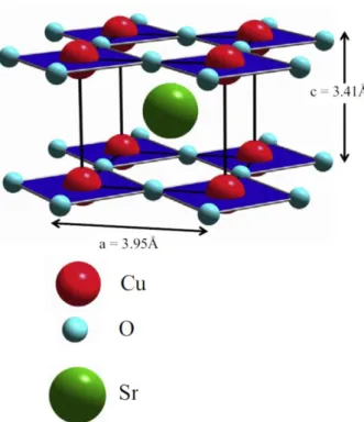
I.4.2.1 Crystallographic structure of infinite-layer cuprates ... 28
I.4.2.2 Properties of (Sr,La)CuO2 ... 30
II
Experimental techniques ... 37
II.1 Deposition technique: Molecular Beam Epitaxy (MBE)... 37
II.1.1.1 Flux measurements: Quartz Crystal Monitor (QCM) .... 39
II.1.1.2 Reflection High Energy Electron Diffraction (RHEED) in-situ diagnostic ... 39
II.1.2 The MBE deposition system present at UNISA ... 42
II.1.3 The MBE deposition system present at Cornell Univesity .... 44
II.2 Standard thin films characterization technique ... 45
II.2.1 X-Ray Diffraction (XRD) technique for thin films structural characterization ... 45
II.2.1.1 XRD theory: Bragg reflection ... 45
II.2.1.2 Thin film measurements configuration: θ-2θ scan and X-Ray Reflectivity (XRR) measurements ... 46
II.2.2 Electrical transport measurements ... 48
II.3 Advanced electron spectroscopy ... 49
II.3.1 X-ray Absorption Spectroscopy (XAS) ... 49
II.3.2 X-ray Magnetic Circular Dichroism (XMCD) ... 53
II.3.3 X-ray Linear Dichroism (XLD) and X-ray Magnetic Linear Dichroism (XMLD) ... 54
Results ... 57
III.1 Growth and characterization of p-type QWs ... 57
III.1.1 Structural characterization ... 61
III.1.2 Electrical transport characterization ... 66
III.1.3 Preliminary results of advanced spectroscopy measurements on p-type QWs ... 72
III.1.3.1 Localization and orbital order in SMO/LSMO/SMO quantum wells... 72
III.1.3.2 Competition between ferromagnetism and antiferromagnetism in SMO/LSMO/SMO heterostructures: towards magnetic oxides quantum wells ... 75
III.2.1 Structural characterization ... 84
III.2.2 Electrical transport characterization ... 87
III.3 Doping effect on the normal and superconductive state of (Sr,La)CuO2... 94
III.3.1 The role of Quantum Interference Effects on the normal state ... 96
III.3.1.1 Noise spectroscopy measurements ... 101
III.3.2 Low temperature hidden Fermi-liquid charge transport in (Sr,La)CuO2 ... 102
III.3.3 X-ray absorption spectroscopy (XAS) study of annealing process on (Sr,La)CuO2 thin films ... 110
Conclusions ... 119
Bibliography... 122
Appendix A. Strong correlations and Hubbard model ... 135
Appendix B. Ginzburg-Landau approach for clean electronic systems 137 Appendix C. Evidence of WL in SLCO films by noise spectroscopy measurements ... 139
IV
List of figures
Figure I-1 Schematic of a semiconductor-based QW as function of distance in the growth direction Z (Odoh and Njapba, (2015))... 2 Figure I-2 Direct and indirect excitons in semiconductor-based QW and DQW ... 3 Figure I-3 Sketch of heterostructure configuration in which a narrow- gap correlated insulator (B) is embedded in two wide band-gap insulators (A and C). The potential drop across the heterostructure is shown in top panel. The band bending presented ad energy E vs momentum k is shown in the bottom panel. μ is the chemical potential (Millis and Schlom, (2010)) ... 4 Figure I-4 a) schematic of a QW with 5 SrVO3 layers embedded in SrTiO3; b) angle-integrated photoemission spectrum, symmetrized with respect to the Fermi energy in function of the number of the central layers (Yoshimatsu et al., (2013), (2010)) ... 7 Figure I-5 Electron Energy Loss Spectroscopy (EELS) in Transmission Electron Microscopy (TEM) map over a wide field of view (the scale bare is 5 nm) for an n = 3 (SMO)n / (LMO)2n grown on SrTiO3 substrate showing La in green, Mn in red and Ti in blue (Monkman et al., (2012)) 8 Figure I-6 (Left) schematic showing an extreme-electron density QW where SrTiO3 is embedded between two layers RETiO3 (RE=Gd,Sm); (Right) Temperature dependent sheet resistance for GdTiO3/SrTiO3/GdTiO3 (top panel) and SmTiO3/SrTiO3/SmTiO3 (bottom panel) as a function of SrTiO3 layer thickness (Zhang et al., (2014))... 9 Figure I-7 Resistivity versus the temperature for LaVO3/SrVO3/LaVO3 trilayers as a function of the central layer thickness, that is 35, 20, 3 monolayers (ML in figure); SrVO3 single layer (black curve) is shown as a reference ... 11 Figure I-8 I-V characteristic of a LaAlO3-SrTiO3 device in function of the tip bias applied (Vtip=0,-0.5,-1,-2,..,-10 V). The top inset is a zoom for
lower voltage. The bottom inset show the turn-on voltage of the nanowire section with a potential barrier as a function of Vtip that is used to create the barrier (Cen et al., (2009)) ... 13 Figure I-9 a) structure of SrTiO3/GdTiO3 HFET; b) optical micrograph of the transistor (Boucherit et al., (2013)) ... 14 Figure I-10 Measured and calculated output characteristic for SrTiO3/GdTiO3 HFET where the gate voltage VG was swept from 0V to -12 V (Boucherit et al., (2013)) ... 15 Figure I-11 Top panel: magnetization versus the temperature and field applied for La0.75Ca0.25MnO3; middle panel: resistivity versus the temperature and field applied; bottom panel: magnetoresistance versus the temperature (Ramirez, (1997)) ... 21 Figure I-12 a) Schematic view of a cubic perovskite structure ABO3; b) orthorhombically distorted perovskite-type structure ... 23 Figure I-13 Jahn-Teller distortion. On the left: 3d-orbitals degeneracy of Mn3+ single ion; in the center: degeneracy partially removed thanks to crystal field (interaction with oxygen octahedrals); on the left: degeneracy further removed thanks to octahedral elongation (Jahn-Teller distortion).25 Figure I-14 A schematic representation of double exchange mechanism in
mixed valence manganites (Dagotto et al., (2001)) ... 26 Figure I-15 Phase diagram of La1-xSrxMnO3 as a function of Sr content x (Dagotto et al., (2001)) ... 27 Figure I-16 IL crystal structure of SrCuO2. The typical values for the lattice parameters are shown as a reference (Fournier, (2015)) ... 30 Figure I-17 Unsymmetrized Fermi surface mapping of optimally doped Sr0.9La0.1CuO2 taken at 10K. The gray and yellows arcs are obtained from theoretical calculations (Harter et al., (2012))... 32 Figure I-18 Doping – temperature phase diagram of cuprate superconductors where the antiferromagnetic (AF) and superconductive (SC) phases are shown both for electron-doping (left) and hole-doping (right). Néel temperature (TN), temperature where the resistivity shows a linear behavior in temperature (T*) and a quadratic behavior in temperature (T**) are indicated for the hole-doped cuprates (right) ... 34 Figure II-1 Effusive cell used in the University of Salerno MBE deposition system. The effusive cells are closed by shutters that can be manually or computer controlled by pneumatic actuators. ... 38 Figure II-2 Schematic diagram of RHEED geometry showing the incident beam to the surface sample with angle θ. ... 40 Figure II-3 SrTiO3 layer-by layer RHEED intensity oscillations acquired on the central streak. The opening of Sr shutter and Ti shutter is indicated.
VI
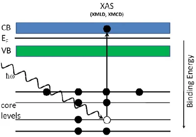
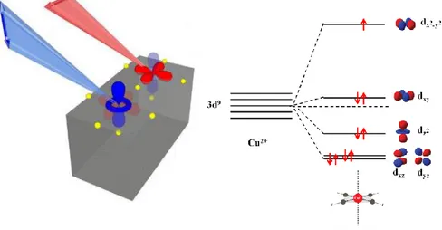
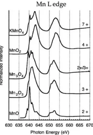
(a) Stoichiometric full monolayer of Sr and Ti deposited; (b) Sr dose is held constant while Ti dose increased by 3% from a full monolayer; (c) Sr dose is held constant while Ti dose decreased by 3% from a full monolayer (Haeni et al., (2000)) ... 42 Figure II-4 A schematic representation of MBE system located at UNISA. 43 Figure II-5 Schematic representation of the MBE system at Cornell University ... 44 Figure II-6 Schematic Bragg’s law depicting the constructive inference of reflected waves ... 46 Figure II-7 Schematic representation of Van der Pauw contacts configuration ... 48 Figure II-8 Schematic representation of XAS mechanism. CB and VB are the conduction and the valence band respectively and EF is the Fermi energy ... 50 Figure II-9 Transitions that contribute to XAS edges ... 51 Figure II-10 Cu 3d states probed by XAS radiation. Left: schematic
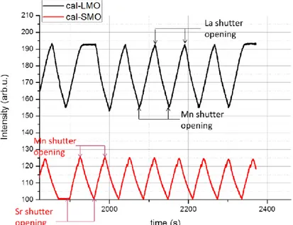
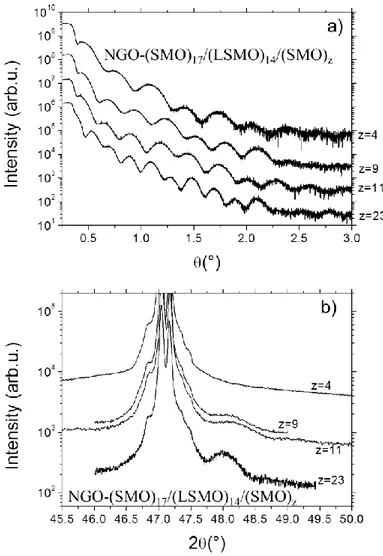
representation of horizontal (red) and vertical (blue) light polarization used to probe in-plane and ou-of-plane states; right: electronic configuration of 3d states of ion Cu2+ ... 52 Figure II-11 Multiplet structure for different oxidation state of Mn (Gilbert et al., (2003)) ... 53 Figure III-1 Layer-by-layer RHEED calibration of LMO and SMO single layers. Sr, La, Mn respective shutters opening is highlighted. ... 59 Figure III-2 Typical RHEED pattern of an epitaxial SMO/LSMO/SMO QW viewed along the [100] azimuth a) and along the [110] azimuth b). Both images are acquired at the end of the growth ... 60 Figure III-3 Structural characterization of SMO/LSMO/SMO QWs in function of the central layer thickness. Curves are shifted for clarity. a) XRR spectra of QWs grown on STO substrate where the top and the bottom SMO insulating layers’ thicknesses are fixed symmetrically at 14u.c. while y=15, 13, 9, 5, 4; for one of the curves a fit of the reflectivity is shown (thick green line). b) XRD spectra of the same samples shown in a). c) XRR spectra od QWs grown on NGO substrate where the top and the bottom SMO insulating layers’ thicknesses are respectively fixed at 15 and 11u.c., while y = 15, 13, 7, 4; for one of the curves a fit of the reflectivity is shown (thick red line). d) XRD spectra of the same samples shown in c) ... 61 Figure III-4 XRD fit of the samples with y= 15, 13, 7 shown in Figure III-3 d), in comparison with the their tween samples grown on STO substrates
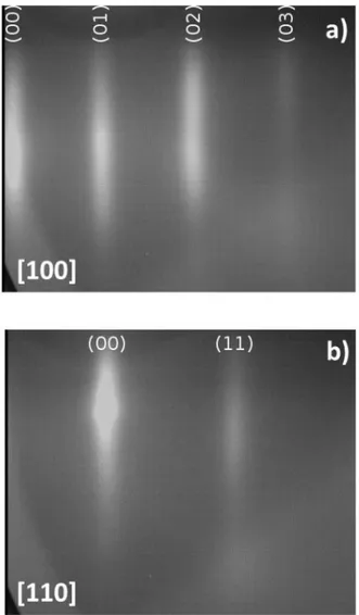
in the same deposition run. SMO single layers on STO and on NGO are also reported. Zooms of (002) reflection are shown in insets. ... 63 Figure III-5 Structural characterization of SMO/LSMO/SMO QWs in function of the topmost SMO layer’s thickness. Curves are shifted for clarity. a) XRR spectra of QWs grown on NGO substrate where the insulating SMO bottom layer and the central LSMO metallic layer thicknesses are fixed respectively at 17u.c. and 14u.c. while z=23, 11, 9, 4; b) XRD spectra of the same samples shown in a) ... 65 Figure III-6 Resistivity versus temperature curves of QWs with different topmost SMO layer thickness z in unit cells ... 67 Figure III-7 Resistivity versus temperature curves normalized to room temperature, 300K, of QWs samples grown on STO (a) and on NGO (b) with different LSMO layer thickness y in unit cells; the curves are vertically shifted by a constant offset factor for clarity. ... 69 Figure III-8 a)Metal to insulator transition temperature TMI as a function of LSMO layer thickness y. The shadowed region indicates the thickness at which insulating behavior emerges at low temperature. b) resistivity minimum temperature as a function of LSMO layer thickness y. Two different regimes are clearly observed for samples with y > 5 and y ≤ 5. The data points are grouped dependently on minimum position: red line for minima occurring below 50K and blue line for minima occurring above 150K ... 70 Figure III-9 Top panel: sum XAS spectra of single layers of LSMO and SMO; bottom panel: sum XAS spectra of the QWs as a function of the topmost SMO insulating layer z ... 74 Figure III-10 a) ratio of XMCD intensity in GI and NI at 20 K and 250 K, with an applied magnetic field of 2T; b) XMLD spectra of the samples with (full lines) and without (dashed lines) the application of magnetic field in the beam direction... 77 Figure III-11 RSXS measurements performed on the y=15u.c. e and on the y=4u.c LSMO central layer thicknesses acquired at 100K. ... 79 Figure III-12 Layer-by-layer shutterd RHEED calibration on SCO. In the top panel a RHEED pattern during the calibration is shown. The intensity is acquired on the diffracted rod [10] (blue box and line) and on the incommensurate rod (red box and line). ... 82 Figure III-13 Typical RHEED pattern of a epitaxial QWs viewed along the [110]p azimuth at the end of growth (a) and after the vacuum annealing step (b). In (a) white arrows highlight extra diffraction streaks present in all as-grown films ... 83
VIII
Figure III-14 a) XRR spectra of single layers (SCO and SLCO) and of the trilayers with different SLCO thickness (y=20, 15, 10, 4 and 3), as a function of the incident angle θ. A fit of the reflectivity is shown for the sample with y=5; b) XRD spectra of the samples shown in a) ... 85 Figure III-15 Simulation of the XRD spectra for the trilayer with SLCO y=20 (red curve) and SLCO single layer (grey curve) ... 87 Figure III-16 Sheet resistance Rsheet vs temperature T curves of trilayered samples with different SLCO layer thickness y in unit cells... 88 Figure III-17 Critical onset temperature TConset as a function of y where the blue curve is the best fit using eq. III-3. In inset, the behavior and the linear fit (red lines) of TConset as a function of 1/y (left) and of 1/y2 (right) are shown ... 90 Figure III-18 a) linear fit (red curves) of the low temperature (below 40K) conductivity for the samples with y =3 as a function of ln(T) (top) and T3/2 (bottom); b) linear fit (red curves) of the low temperature (below 40K) conductivity for the samples with y = 4 as a function of ln(T) (top) and T3/2 (bottom). ... 93 Figure III-19 Two magnification of TEM image of SLCO thin film grown on a TbScO3 substrate. Abrupt interface is observable, without diffusion and absence of defects, confirming the epitaxial growth of the samples 95 Figure III-20 Resistivity curves for three selected under-doped SLCO samples. The best-fit curves are also reported. Arrows indicate the temperatures below which the resistivity curves are no longer purely linear, namely T*... 97 Figure III-21 Resistivity curve for a representative SLCO sample characterized by an electronic doping close to optimal condition. The fitting curves are also reported. Arrow in the main panel indicates the temperature below which the resistivity curves are no longer purely linear; in the inset, the resistivity behavior and fitting curves are magnified in proximity of the superconducting transition (arrow indicates the lower limit of fitting range) ... 100 Figure III-22 Sheet resistivity as a function of temperature and doping .... 103 Figure III-23 Doping dependence of T*, T** and TConset of the investigated samples; the dashed lines describe the behavior of T* and T** ... 105 Figure III-24 𝐴2⧠ values obtained by fitting the resistivity curves with eq. III-11 (blue triangle) and with eq. III-12 (green stars) ... 107 Figure III-25 Doping dependence of a) 𝐴0⧠ and b) 𝐴𝑙𝑜𝑔⧠ obtained by fitting the resistivity with eq. III-8; c) scaling relation between 𝐴𝑙𝑜𝑔⧠ and 𝐴0⧠. The power-law exponents are reported as insets... 108
Figure III-26 a) 1/RH data obtained for an underdoped sample; b) resistivity after subtraction of fitted logarithmic contribution; c) cotangent of Hall angle (the dashed red line indicate 𝑐𝑜𝑡𝜃𝐻 ∝ 𝐶2𝑇2) ... 110 Figure III-27 (a) XRD spectra as a function of in-situ annealing duration, a zoom of (002) diffraction peak showing a minor variation in the position of the peak for 15-60 min annealed samples is shown in inset; (b) resistivity as a function of the temperature and of annealing of the samples in (a), a zoom of superconductive transition showing that the optimized annealing duration is 30 min is shown in inset ... 113 Figure III-28 (a) XAS Cu L3 edge spectra with H polarization and incident angle of 90° (red filled symbols) and 30° (black hollow symbols) of the as-grown and in-situ annealed samples; (b) normalized XLD at XASISO spectrum of Cu L3 spectra of the as-grown, 5 min and 20 min Ar annealed and in-situ annealed sample. The spectra are vertically shifted for clarity115 Figure III-29 Position of the maximum of Cu L3 XASISO (red circles)and
XLD (black squares) as a function of the normalized XLD intensity maximum ... 116 Figure III-30 Comparison of O K edge XAS spectra of as grown and in-situ annealed samples ... 117 Figure A-1 Schematic diagram of the density of states of the cuprates at increasing levels of details. (a) non-interacting case; (b) Hubbard correlations considered (insulating case); (c) in transition-metal compounds; (d) further hybridization (Harter, (2013)) ... 136 Figure C-1 Low-frequency voltage spectral densities for an under-doped SLCO sample at two different temperatures and at different dc bias currents (i.e., up to 10 mA). The zero-bias background noise is shown as black trace. ... 140 Figure C-2 a) Temperature dependence of the three fitting parameters a2,a1, and a0 appearing in eq. C-1; b) a clear sign of a crossover is evident at Tcross ∼ Tloc ∼ 110 K, where weak localization effects occur producing an upturn of the resistivity and a change of the current power exponent η of the 1 / f noise ... 141
X
List of tables
Table III-1 Properties of the investigated QWs with different LSMO layer thickness y ... 68 Table III-2 Properties of the investigated n-type QWs with different SLCO layer thickness y ... 91 Table III-3 Normalized χ2 values for SLCO samples shown in Figure III-20; data refer to the fitting procedure by using the 2D (eq. III-4) and 3D (eq. III-5 with the different exponent p) localization terms, respectively ... 98 Table III-4 Statistical χ2 values as well as best-fit parameters for the optimally doped SLCO sample shown in Figure III-21. ... 101 Table III-5 Main structural and electrical transport values for the investigated samples ... 104
Abstract
he main goal of this dissertation is the study of the effects induced by quantum confinement in transition-metal oxides quantum wells (QWs). The field of possible applications of oxide-based heterostructures (oxide-based nanoelectronics, spintronics, quantum computation, excitonic devices, energy conversion in solar cells, etc.) is very ample and growing, thanks to the many fascinating and exotic properties of transition-metal oxides and their versatility as well.
p-type SrMnO3/La0.7Sr0.3MnO3/SrMnO3 QWs and n-type SrCuO2/Sr0.9La0.1CuO2/SrCuO2 QWs have been studied.
The first part of my work has been devoted to the investigation of quantum confinement achievement using a Mott insulator with a small band gap. The observed results suggest that this type of material can be successfully used in QWs.
As a final result of my work, the achievement of dimensional effects induced by the layering on the normal state of both investigated systems (n and p-doped) has been assessed. In addition, the layering has been shown to influence the superconducting state of the investigated n-doped QWs and on the metal-to-insulator transition of the p-doped QWs.
The investigation of the behavior of each layer constituent the QW (both n and p-doped) is relevant in view of future growth of proximate p-n doped systems. Part of my work, therefore, has been devoted to the study of the properties of (Sr,La)CuO2 thin films.
The study of electrical transport properties of SLCO thin films as a function of the doping has allowed to relate the presence of the low temperature upturn in the (Sr,La)CuO2 resistivity versus temperature curves the quantum interference effects produced by weak localization effects. Furthermore, the presence of low temperature Fermi liquid behaviors in SLCO thin films has also been observed.
XII
The last part of my work has dealt with the effects of the in-situ annealing step on the final superconductivity properties of the (Sr,La)CuO2 films, helping to optimize the growth step, crucial for the quality of this thin film and, consequently, of the n-doped QWs based on this compound. The effect of annealing, i.e. of the O content, has been studied, by using X-ray Absorption Spectroscopy (XAS) measurements performed at the Elettra Synchrotron in Trieste, Italy, and has allowed to reveal clear signature of apical Oxygen removal.
Introduction
uring this Ph.D. work, I have investigated the effects induced by quantum confinement in transition-metal oxides (TMO) low-dimensional systems and hetero-structures, such as quantum wells (QWs). An oxide-based QW is the simplest system in which a quantum confinement can be obtained, consisting in a thin layer of one oxide material, sandwiched between two layers of another oxide insulating material (this creates a well in which the carriers can move in two directions but are confined in the third). In these systems it is possible to create and manipulate quantum states of matter, including novel superconductors, high Curie-temperature magnets, controllable metal-insulator transition.
The oxide-based QWs recently raised interest compared to the well-known semiconductors based ones thanks to the possibility to obtain lower dimensional heterostructures (a few nm), higher sheet carrier density (1014 cm-2), one order of magnitude more than the highest density achievable in conventional semiconductors III-nitrides, and many fascinating and exotic behaviors related to the spectacular versatility of the complex oxide interfaces (Stemmer and Millis, (2013)).
The field of possible applications of oxide-based heterostructures (oxide-based nanoelectronics, spintronics, quantum computation, excitonic devices, energy conversion in solar cells, etc.) is very ample and growing, as it will be described in Section I.3, thanks to the many fascinating and exotic properties of TMO and their versatility as well.
The study of oxide-based QWs, and of TMO thin films in general, is possible thanks to the important developments in oxide thin films depositions techniques and in particular in oxide-molecular beam epitaxy (O-MBE) techniques, where atomic-scale thickness control, abrupt interfaces and the possibility to change the chemical composition over a distance of a
XIV
single unit cell, are now achievable (Biegalski et al., (2008); Jalan et al., (2009); Petrov et al., (2004); Schlom et al., (2001)).
Many TMO are Mott insulators (Mott insulators are a class of materials that should conduct electricity under conventional band theories, but experimentally they are insulators. This effect is due to electron–electron interactions, which are not considered in conventional band theory), with small energy band gaps, and the question arises on the ability to obtain quantum confinement by using them as insulating materials in QWs.
The first part of my work has been dedicated to answer this question: p-type SrMnO3/La0.7Sr0.3MnO3/SrMnO3 (SMO/LSMO/SMO) QWs have been grown at University of Salerno by O-MBE deposition techniques and their electrical transport properties have been characterized as a function of the temperature and of the relative thicknesses (Galdi et al., (2017)). The observed results have indicated the presence of spatial charge carrier confinement in the investigated trilayers pointing out the ability of a small gap Mott insulator material, such as SMO, with an energy gap of 0.35 eV (Søndenå et al., (2006)), to be successfully used in QWs.
The following part of my work has been devoted to the study of both the p and n-type oxide-based QWs, which is important because it could open the way to investigate carrier symmetries in such systems and to obtain hybrid p-n proximate structures with the presence of long life-time excitons (hole-electron couples). The availability of both p and n doped oxide QWs to be grown by the same deposition technique in similar deposition processes, involving a minimum number of materials, is central to obtain p-n TMO based proximate structures (Kim et al., (2016); Millis and Schlom, (2010)).
The electron-doped structures I focused my attention are the n-type SrCuO2/Sr0.9La0.1CuO2/SrCuO2 (SCO/SLCO/SCO) QWs, which I have grown during my abroad experience at Cornell University, Ithaca, NY-USA. The fabrication of low dimensional systems with high superconductive critical temperature (TC), such as electron-doped infinite-layers SLCO, confined to nanometer-sized interfaces, is an intriguing issue by itself, due to the possibility to study a paradigmatic quantum phenomenon, such as superconductivity in reduced dimensionality, and to exploit its potential application (Ahn et al., (2003), (1999); Gozar et al., (2008); Mannhart and Schlom, (2010)).
As a final result of my work, the achievement of dimensional effects induced by the layering on the normal state of both investigated systems (n and p-doped) has been assessed. In addition, the layering has been shown to
influence the superconducting state of the investigated n-doped QWs and on the metal-to-insulator transition of the p-doped QWs.
The growth and characterization of QWs implies the preventive study of the behavior of the metallic single layers (LSMO for the p-doped QWs and SLCO for the n-doped QWs).
Such investigations are relevant especially in view of the future growth of proximate p-n doped DQWs. In fact, one of the advantages to use TMO-based QWs rely on the possible tuning of the density of carriers changing the doping level of the central layer. This will offer two controlled knots (i.e. the central layer thickness and its doping) to tune the interaction among electrons and holes improving the final versatility of the applicative device.
This part of my work, with the further investigation of the normal state transport properties of SLCO thin films, has pointed out new interesting behaviors. In particular, despite the considerable efforts of the scientific community, a conclusive understanding of the normal-state transport properties of electron-doped cuprates is still missing and the results obtained in this work on SLCO thin films having the simplest crystal structures with CuO2 planes that hosts high-TC superconductivity, have clarified some aspects of this existing puzzling scenario.
In particular, the study of electrical transport properties of SLCO thin films as a function of the doping has allowed to relate the presence of the low temperature upturn in the SLCO resistivity versus temperature curves the quantum interference effects produced by weak localization effects (Barone et al., (2016); P Orgiani et al., (2015)). Furthermore, the presence of low temperature Fermi liquid behaviors in SLCO thin films have also been observed.
The last part of my work has dealt with the effects of the in-situ annealing step on the final superconductivity properties of the SLCO films. These are strongly affected by sample preparation conditions and a reduction process is needed for all electron doped cuprates thin films in order to get superconductivity.
The optimization of this step is, therefore, crucial for the quality of SLCO thin films and, consequently, of the n-doped QWs based on this compound. The effect of annealing, i.e. of the O content, has been studied, by using X-ray Absorption Spectroscopy (XAS) measurements performed at the Elettra Synchrotron in Trieste, Italy, and has allowed to reveal clear signature of apical Oxygen removal.
This dissertation is organized as following: in the Chapter I, I describe the quantum confinement in QWs and the importance of innovative material for
XVI
QWs (Section I.1). The most important results on oxide-based heterostructures already present in scientific literature are also highlighted (Section I.2). Section I.3 is dedicated to the potential application of oxide-based heterostructures. In Section I.4 the main properties of Mn and Cu oxide-based compounds are described in details, focusing on their crystal and electronic structure and on their respective phase diagrams as well.
In Chapter II, the experimental techniques are described: deposition techniques (Sections II.1), standard thin film characterization methods (i.e. XRD measurements for structural characterization and electrical transport measurements) (Section II.2) and advanced electron spectroscopic techniques (i.e. X-rays absorption spectroscopy both in presence and absence of magnetic field) (Section II.3).
Chapter III deals with the experimental results. In the first part I describe the results about the growth and characterization of p-type QWs (Section III.1). In particular, I describe the structural and electrical transport measurements as a function of the layer thicknesses, discussing the evidences of the quantum confinement (Sections III.1.1 and III.1.2). Furthermore, preliminary results about advanced spectroscopy measurements performed on p-type QWs are provided (Section III.1.3).
The deposition and characterization of n-type QWs is described in Section III.2. In particular, the structural and electrical transport characterizations done on these samples are described in Sections III.2.1 and III.2.2.
In the last Section, the doping effects on the normal and superconductive state of single layers SLCO thin films are analyzed (Section III.3), along with X-ray absorption spectroscopy measurements performed to study the effects of the annealing process (Section III.3.3).
Quantum confinement in
Quantum Wells
I.1 Innovative materials for Quantum Wells
ith the need of reducing dimensionality and, at the same time, of increasing the speed of conventional semiconductor-based micro and opto-electronic devices, scientific limitations are beginning to affect the newer device demands of modern times. Novel approaches involving new materials such as functional oxides are being explored for new concept of electronic devices. These innovative materials are interesting for new physics and novel functionalities arising from ultrathin oxide films and at oxide interfaces in their heterostructures, such as Quantum Wells (QWs). A QW is the simplest system in which a quantum confinement can be obtained and these systems are generally based on semiconductor science and technology. Quantum confinement involves the use of spatial modulation of chemical composition and electric fields to localize electrons to regions that are sufficiently small that their quantum mechanical properties are affected. An illustration of a semiconductor-based QW is shown in Figure I-1, where a thin semiconductor layer of lower band gap material (e.g. InGaN) is sandwiched between two thick semiconductor layers of larger band gap (e.g. GaN). This creates a potential well in which the carriers can move in two
2
directions but are confined in the third. These devices have replaced the conventional electronic components in QW lasers, QW detectors, QW modulators and so on (Odoh and Njapba, (2015)).
Figure I-1 Schematic of a semiconductor-based QW as function of distance
in the growth direction Z (Odoh and Njapba, (2015))
The basic idea of a QW, as shown in Figure I-1, can be also realized with the transition metal oxides (TMOs) which offer a very rich physics: electrons in the narrow d-band of TMOs are subject to strong electron-electron interaction (correlated electrons) and this leads to a rich variety of physical phenomena that can be controlled, modified and tuned in an oxide-based QW (e.g. magnetism with high Curie temperature, metal-to-insulator transitions, high critical temperature superconductivity).
TMOs can be doped with electrons (n) or holes (p) as well as semiconductors, but these materials are good candidate to improve the performance of semiconductor-based devices. In fact, compared with semiconductor-based devices, it is possible to achieve very small devices (with dimensions of few nm), high electron densities required to obtain the Mott insulators are very high (on the order of 1022 cm-3) and sheet carrier densities on the order of 1014 cm-2 in a single atomic plane are observable (Ahn et al., (2006)). Such sheet carrier densities are an order of magnitude higher than the highest density of two-dimensional gases (2DEGs) based on conventional semiconductors (III-nitrides) (Stemmer and Millis, (2013)).
The study of proximate n-p doped oxide-based structures to create and control electron-hole bound states, i.e. excitons, is a very intriguing topics in the physics of condensed matter. Excitons are relevant in many process and their possible manipulation can have important consequences in many
applications (for example, the energy conversion in solar cells) and even in the opening of completely new applicative field such as the excitonics (i.e. the electronics based on excitons).
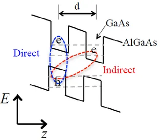
Over the years, considerable effort has been invested in optically generated electron-hole liquids (Butov et al., (2002); Ideguchi et al., (2008)), but creating and manipulating sufficiently high-density while preventing the electron-hole recombination has proven challenging. In order to prevent fast recombination and to increase the exciton mean life as well, Zhu et al. proposed to construct a double quantum well (DQW) system in which one QW contains holes and the other contains electrons, as described in Section I.3.3. The spatial separation prevents recombination and it is possible to tune the interaction between electrons and holes by adjusting the distance between the two QWs (Littlewood and Zhu, (1996); Zhu et al., (1995)). The bound states in this way generated are known as indirect excitons.
Figure I-2 Direct and indirect excitons in semiconductor-based QW and
DQW
DQWs can be fabricated in semiconductor systems such as (Al,Ga)As, as shown in Figure I-2, but the large band gap of these materials requires a too large bias to effectively produce acceptable equilibrium in electron and hole populations (Millis and Schlom, (2010)). A.J. Millis and D. G. Schlom in 2010 proposed an interesting route to the formation of proximal electron and hole liquids, regarding an oxide heterostructure involving a thin layer of narrow gap correlated insulator, such as a Mott insulator (B in Figure I-3) ,
4
sandwiched between two different wide-band-gap insulator (A e C in Figure I-3). If AB and AC interfaces are polar and if charge reconstruction is absent (Okamoto and Millis, (2004)), an internal electric field can be generated, leading to a potential drop which scales linearly with the thickness of the correlated material (top panel in Figure I-3). The potential drop causes band bending which, if large enough, shifts the conduction band below the Fermi level on one side of the structure and the valence band above the Fermi level on the other side (bottom panel in Figure I-3), creating electron and hole accumulation respectively.
Figure I-3 Sketch of heterostructure configuration in which a narrow- gap
correlated insulator (B) is embedded in two wide band-gap insulators (A and C). The potential drop across the heterostructure is shown in top panel. The band bending presented ad energy E vs momentum k is shown in the bottom panel. μ is the chemical potential (Millis and Schlom, (2010))
Mott insulators are particularly attractive candidates because of their properties. Indeed, they often have relatively small gaps 2Δ~0.3-2 eV (Imada et al., (1998)), so the electric field required to produce the needed band bending doesn’t need to be prohibitively large. In addition, the physics of correlated materials is local, that is the relevant length scales for charge
phenomena are of the order of a unit cell while interlayer coupling are intrinsically weak (such as the parent compound of high superconductive critical temperature) or can be made weak inducing appropriately orbital ordering.
Several research groups have investigated the possibility of creating oxide-based QWs and DQWs. In the following Section, I will describe some of the most important results on this issue already present in scientific literature, where, in some systems, evidence of quantum confinement is observed. Nevertheless, a control of the properties related to the quantum confinement, as well as a control on the density of states, and consequently of the carriers, is not realized yet.
The QWs investigated in this work consist in a metallic layer known to be electron (Sr0.9La0.1CuO2) or hole-doped (La0.7Sr0.3MnO3) embedded in insulating materials, respectively SrCuO2 and SrMnO3. The peculiarities of these compounds will be described in detail in Section I.4.
The relevance of these systems is not only related to the study of their properties as a function of the relative thickness of each layer or to a future development of growing proximate n-p doped DQWs, but also to the possibility to tune the density of carrier changing the doping level of the central layer. In view of future devices development, the possibility to tune the interaction between the carriers thanks to the simple modulation of the layer thickness and of the carrier concentration (i.e. through the doping) is a key issues for the versatility of applications, as it will described in Section I.3.
I.2 Materials and examples of oxide-based QWs in literature
Experimentally, the scientific community has been concentrated largely on perovskite-structured TMO with the chemical formula ABO3, where the B site ion is a transition metal with partially filled d-shell (or empty in case of SrTiO3) and is octahedrally coordinated with six oxygen ions, while the A site ion is typically an alkali earth (e.g. Ca, Sr, Ba) or a trivalent rare-earth ion (e.g. La, Ce, Nd). The A site ion fills the d-shell donating two (for alkali earth) or three electrons (for lanthanides).
QWs studied until now have been created by spatial variation of electrochemical potential in several ways. One is by varying the A-site ion for example sandwiching a few layers of LaMnO3 (LMO) between layers of
6
SrMnO3 (SMO). In this way, the difference in charge between La3+ and Sr2+ ions create a spatially varying electrical potential causing a spatially varying electron density. Another choice is to vary the B-site ion, for example sandwiching a few layers of SrVO3 between layers of SrTiO3. In this example, the different electronegativities of V and Ti define the QW.
I.2.1 SrTiO
3/SrVO
3/SrTiO
3QWs
QW consisting in n layers of SrVO3, that is a conductive oxide and moderated correlated material with cubic perovskite structure, embedded in SrTiO3, that is a cubic perovskite band insulator, have been studied by Yoshimatsu et al. using photoemission spectroscopy (Yoshimatsu et al., (2013), (2011), (2010)). Using this technique, it is possible to measure the occupied portion of electronic density of states. Yoshimatsu et al. observed that the photoemission spectra remain quite similar to that of bulk material down to approximately six unit cells of SrVO3. Below this thickness, changes become apparent. Indeed, a suppression of the density of states peak at Fermi level is observable in Figure I-4 b). This behavior has been associated to quantum confinement effect. In particular, it has been observed that the quantum confinement can qualitatively alter the electronic properties but confinement effects become detectable only at very short length scale that, in this case, is less than six unit cell thickness.
Figure I-4 a) schematic of a QW with 5 SrVO3 layers embedded in SrTiO3;
b) angle-integrated photoemission spectrum, symmetrized with respect to the Fermi energy in function of the number of the central layers (Yoshimatsu et al., (2013), (2010))
I.2.2 LaMnO
3/ SrMnO
3superlattices
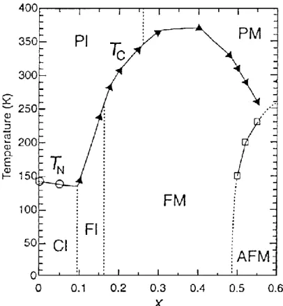
In this structure LMO and SMO layers are alternated defining set of QW. The different ionic charge of La3+ and Sr2+ mean that in bulk LMO, the nominal Mn configuration is d4, while in bulk SMO is d3. SMO is an
antiferromagnetic Mott insulator, while LMO exhibits a strong Jahn-Teller distortion. This lead to a layered antiferromagnetic structure consisting of ferromagnetic planes with alternating spin orientations.
Adamo et al. studied (SMO)n/(LMO)2n and they found that, although the
single layers SMO and LMO are both antiferromagnetic insulators, for n ≤ 2 the superlattice behaves like the ferromagnetic conductor La0.7Sr0.3MnO3 (LSMO). As n increase, the magnetic properties become dominated by LMO
8
layers, but the electronic properties continue to be controlled by interfaces (Adamo et al., (2009b), (2008); Aruta et al., (2009a); Galdi et al., (2012); Monkman et al., (2012)).
Santos et al. fabricated similar superlattice and studied the magnetization profile in these systems. They observed that the length scale over which the magnetization changes from an high to low value is about two unit cells (Santos et al., (2011)). This means that electronic properties can be controlled in QWs.
Figure I-5 Electron Energy Loss Spectroscopy (EELS) in Transmission
Electron Microscopy (TEM) map over a wide field of view (the scale bare is 5 nm) for an n = 3 (SMO)n / (LMO)2n grown on SrTiO3 substrate showing La
in green, Mn in red and Ti in blue (Monkman et al., (2012))
I.2.3 SrTiO
3based QWs
Two-dimensional electron gases at interfaces between SrTiO3 and RETiO3, where RE is a rare-earth, exhibit an extremely high electron densities (~1014 cm-2) that are introduced into the d-bands of SrTiO3.
Moetakef et al. and Zhang et al. investigated the correlation physics via dc-resistivity measurements of two-dimensional electron liquids that reside in narrow SrTiO3 QWs. They studied the behavior of SrTiO3 sandwiched between the Mott insulator GdTiO3 (GdTiO3/SrTiO3/GdTiO3) (Moetakef et al., (2012a); Zhang et al., (2014), (2013)).
The SrTiO3/GdTiO3 interfaces have strong polar discontinuity producing a sheet density of ~3.3•1014 cm-2 per interfaces (Moetakef et al., (2011)). This kind of QWs show a metal-to-insulator transition when their thickness is reduced to 3 SrTiO3 layers (Figure I-6 top), while SmTiO3/SrTiO3/SmTiO3 QWs, where SmTiO3 is a Mott insulator as well, keep to be metallic also for 1 SrTiO3 layer (Figure I-6 bottom) (Jackson et al., (2014); Zhang et al., (2014)).
Figure I-6 (Left) schematic showing an extreme-electron density QW where
SrTiO3 is embedded between two layers RETiO3 (RE=Gd,Sm); (Right)
Temperature dependent sheet resistance for GdTiO3/SrTiO3/GdTiO3 (top
panel) and SmTiO3/SrTiO3/SmTiO3 (bottom panel) as a function of SrTiO3
layer thickness (Zhang et al., (2014))
The metallic behavior of both QWs shown in Figure I-6 is due to the high electron gas density that is confined in SrTiO3 by the band offset.
10
In particular, the different behavior shown in Figure I-6 for low SrTiO3 thickness (less than 3 layers) in GdTiO3/SrTiO3/GdTiO3 QWs compared with SmTiO3/SrTiO3/SmTiO3 QWs has been associated by the authors to structural octahedral distortion at the GdTiO3/SrTiO3 interface, where the electron system abruptly localizes showing an insulating behavior.
This means that metal-to-insulator transition can be induced by structural distortion.
Moreover, in GdTiO3/SrTiO3/GdTiO3 QWs Moetakef et al. observed that GdTiO3/SrTiO3 interface not only give rise to distortion in the insulation SrTiO3 but also to ferromagnetism below a critical thickness absent in bulk (Moetakef et al., (2012b)).
I.2.4 LaVO
3/SrVO
3/LaVO
3heterostructures
The structure and resistive properties of SrVO3 sandwiched between two insulating LaVO3 as a function of the thickness of the central layer (between 3 and 35 monolayers) have been investigated by Li et al. SrVO3 is a correlated 3d1 metal oxide with a cubic symmetry and a T2-dependent resistivity of a Fermi liquid; LaVO3 was used as insulating materials because of the small lattice mismatch and the absence of interdiffusion down to the limit of some monolayers.
The sample with the thickest SrVO3 layer shows a bulk-like metallic behavior, while the thinnest one show a weak localization regime observed below 100 K with a logarithmic temperature dependence. Angular-dependent magnetoresistance measurements showed a two-dimensional transport in the thinnest sample. The modification of the charge properties by the reduced thickness of SrVO3 were underlined by the appearance of a relatively strong positive magnetoresistance under a magnetic field perpendicular to the sample surfaces.
As shown in Figure I-7, all the samples, therefore, present a metallic behavior above 100 K. Furthermore, the resistivity value of the sample with 3 monolayers at room temperature is only a factor of 2 higher than the reference sample, so the reduction of thickness doesn’t influence essentially the conducting properties at room temperature.
Even the thinnest buried layer shows a metallic behavior, entering a weakly localized regime only at low temperature (Li et al., (2015)).
Figure I-7 Resistivity versus the temperature for LaVO3/SrVO3/LaVO3
trilayers as a function of the central layer thickness, that is 35, 20, 3 monolayers (ML in figure); SrVO3 single layer (black curve) is shown as a
reference (Li et al., (2015))
I.3 Potential application of oxide-based heterostructures
In this Section, the potential application of oxide-based heterostructures are described paying attention, in particular, to the current state-of-art about theoretical modeling and new oxide-based devices.
I.3.1 Oxide nanoelectronics
Electronic confinement at nanoscale dimensions is increasingly challenging as the dimensionality and size scale are reduced. The interface between polar and nonpolar semiconducting oxides displays remarkable properties ascribable at modulation-doped semiconductors (Mannhart and Schlom, (2010); Ohtomo et al., (2002); Ohtomo and Hwang, (2004); Thiel et al., (2006)).
12
Cen et al. used LaAlO3-SrTiO3 heterostructures to create tunnel junctions and field-effect transistors with characteristic dimensions as small as 2 nm. These electronic devices can be successfully modified or erased, as shown in their work (Cen et al., (2009)), controlling the confinement using an atomic force microscope lithography technique. These nanoelectronic devices operates at the interfaces between a non-magnetic polar (LaAlO3) and a nonpolar (SrTiO3) oxide band insulators. Indeed, the discovery of a quasi two-dimensional electron gas (q2DEG) at the interface between these two materials, i.e. LaAlO3 and SrTiO3, has raised expectations in oxide electronics, thanks to the extraordinary properties observed. For example, a metal-to-insulator transition can be achieved at room temperature by electric field gating (Thiel et al., (2006)).In these systems, when the thickness of the polar insulator exceeds a critical value, because of polarization discontinuity at the interface, the potential difference across LaAlO3 generates a “polarization catastrophe” and induce the formation of q2DEG at the interface joining the two insulators (Salluzzo, (2015); Thiel et al., (2006)).
Figure I-8 I-V characteristic of a LaAlO3-SrTiO3 device in function of the tip
bias applied (Vtip=0,-0.5,-1,-2,..,-10 V). The top inset is a zoom for lower
voltage. The bottom inset show the turn-on voltage of the nanowire section with a potential barrier as a function of Vtip that is used to create the barrier
(Cen et al., (2009))
Furthermore, an electric-field-tunable spin polarized and superconducting quasi-2D electron system can be created in LaAlO3/SrTiO3 heterostrucutures by introducing a few atomic layers of EuTiO3, that is an antiferromagnetic insulator with the same structure of SrTiO3. Signature of unconventional superconductivity has also been observed in LaAlO3/SrTiO3 heterostrucutures, using nanoscale Josephson junction devices. The advantages and the possibility to create and study unconventional superconducting states is another support to the fascinating possibilities offered by engineered oxides for realizing novel quantum electronics (Stornaiuolo et al., (2017), (2016))
Boucherit et al. proposed to exploit the high carrier density at SrTiO3/GdTiO3 interface. Such interfacial electron gases can be used to design innovative oxide electronic devices, such as heterostructure field-effect transistors (HFETs), shown in Figure I-9.
14
Figure I-9 a) structure of SrTiO3/GdTiO3 HFET; b) optical micrograph of
the transistor (Boucherit et al., (2013))
Three terminal measurements were carried out on the SrTiO3/GdTiO3 HFET. The measured output characteristic of the device are shown in Figure I-10 and, for the available gate voltage range (VG was swept from 0V to -12 V), there is a total current modulation of 20.3%. The field effect mobility of 5 cm2 V-1 s-1 was extracted. The gate leakage was much lower than the drain current (Boucherit et al., (2013))
Figure I-10 Measured and calculated output characteristic for
SrTiO3/GdTiO3 HFET where the gate voltage VG was swept from 0V to
-12 V (Boucherit et al., (2013))
I.3.2 Spintronics
In conventional electronics, information is related to the electron charge, while, in spintronics, the electron spin is used as an additional degree of freedom to perform logic operation, store information, etc., exploiting the spin-dependent electronic properties of magnetic materials and semiconductors (Bibes and Barthelemy, (2007); Žutić et al., (2004)).
Spintronic systems are of particular interest for quantum computing, in which electron spins in quantum confined structures play the role of the quantum bits (qubits). Indeed, every spin 1/2 encodes exactly one qubit (Awschalom et al., (2002)).
Experiments have supported the idea to use spin as an additional degree of freedom in electronics, showing, e.g., long spin dephasing times in semiconductors QWs and phase-coherent spin transport over distances of up to 100µm (Kikkawa et al., (1997); Kikkawa and Awschalom, (1998)). New mechanisms for information processing can be found in conventional devices (Wolf et al., (2001)) as well as in quantum confined structures used
16
for quantum computing (Loss and DiVincenzo, (1998)). In conventional devices, in fact, the electron spins can improve the performance, e.g. in spin-transistors, non-volatile memories, etc. (Awschalom et al., (2002)).
Oxide-based heterostructures can be used in spintronics. The main interest in this field is the possibility to obtain ferromagnetic insulator ultrathin films usable as tunnel barriers that can filter electrons selectively according to their spins, known as spin filters (Bibes et al., (2011)).
Another spintronics effect that gives rise to a large number of experimental and theoretical studies is tunnel magnetoresistance (TMR). TMR is a magnetoresistive effect that occurs in a magnetic tunnel junction, which consists in two ferromagnets separated by a thin (typically a few nm) insulator. This effect is also the basis of non-volatile magnetic random access memories (MRAMs). The large variety and tenability of the physical properties exhibited by TMOs such as perovskites (e.g. ferroelectricity, ferro- and antiferromagnetism, superconductivity, metallicity, optical properties, etc.) can be exploited in spintronics. Large TMR can be obtained using special magnetic materials (the so-called half-metals), which have a finite density of states at the Fermi level for one spin direction and a gap for the other spin direction (Bibes and Barthelemy, (2007)).
The first pioneering results about the TMR were obtained by Lu et al. on tunnel junctions based on manganese perovskite oxides (La0.67Sr0.33MnO3/SrTiO3/La0.67Sr0.33MnO3 trilayers) (Lu et al., (1996)), and then the interest for oxides in spintronics has increased. Indeed, new families of magnetic oxides, namely, diluted magnetic oxides and multiferroics, have emerged and started to reveal their potential for spintronics.
The relevance of oxides to spintronics is not restricted to generating highly spin-polarized currents. Approaches to exploit their multifunctional character are promising and reveal new physical phenomena. Other promising approaches for oxide-based electronics and spintronics rely on engineering interfaces between two oxides to design 2D phases with novel electronic properties (Bibes and Barthelemy, (2007)). For example, LaAlO3/SrTiO3 systems, presented in the previous section, besides their potential for electronics, the high electronic mobility and 2D character make this quasi-2D electron system an interesting platform to explore lateral spin transport (spintronics) in oxide heterostructures. Measurements performed by Rayren et al. on a LaAlO3/SrTiO3 device showed efficient spin injection at the interface, using a back-gate voltage that modulates the density of states at the interface. In particular, the efficiency of spin injection into the quasi-2D electron system at the LaAlO3/SrTiO3 interface is discussed in terms of
coupling tunnel resistance with localized electronic states controlled by the application of a back-gate voltage (Reyren et al., (2012)).
I.3.3 Excitonic devices and excitonic quantum computation
Already in 1968, Kaldysh and Kozlov showed that in semiconductors with low excitonic density, i.e. 𝑛𝑒𝑥𝑎𝐵𝑜ℎ𝑟𝐷 ≪ 1 where 𝑛𝑒𝑥 is the excitonic density, 𝑎𝐵𝑜ℎ𝑟 is the effective Bohr radius and D is the system dimensionality, the fermionic nature of excitons can be ignored. Indeed, they behave as a weakly non-ideal Bose gas and at a critical temperature TC the
can form a Bose-Einstein condensate (BEC). In particular, for a three-dimensional system the TC is given by:
𝑘𝐵𝑇𝐶3𝐷 =
3.31ℏ2𝑛𝑒𝑥 2/3 𝑚𝑒𝑥
where 𝑚𝑒𝑥 is the exciton mass. If the 𝑚𝑒𝑥 is small, the expected transition temperature can be relatively higher than those typical of atomic BEC. TC is
also dependent on the exciton density and increases with increasing 𝑛𝑒𝑥 values (Keldysh and Kozlov, (1968)). In a semiconductor, the electron (hole) density can be controlled in certain ranges by suitably doping with donors (acceptors). Unfortunately, because of increased role played by the Pauli exclusion principle art educe electron-electron (hole-hole) distances, increased values of the electron (hole) density, and therefore 𝑛𝑒𝑥, also imply that the fermionic nature of the electron-hole pairs cannot be any longer ignored. In the high density limit, i.e. 𝑛𝑒𝑥𝑎𝐵𝑜ℎ𝑟𝐷 ≫ 1, excitons start to be similar to Cooper pairs and their condensation is analogous to a Bardeen-Cooper-Schrieffer (BCS) superconducting state (Conduit et al., (2008); Keldysh and Kopaev, (1965); Pieri et al., (2007)). The electron (hole) density, and the related role of the Pauli exclusion principle, is also crucial for the value of the ratio between the Coulomb interaction and the kinetic energy 𝑟𝑆, which determines the character of the system. In fact, it is known that in a system of 2D electrons or hole, low 𝑟𝑆 values (i.e. 𝑟𝑆≈ 1) characterize a gas-like system, while intermediate values (i.e. 𝑟𝑆≈ 10) are associated to a liquid-like behavior and high values (i.e. 𝑟𝑆≈ 40) described the so called “Wigner crystal” solid. The electron (hole) density n and 𝑟𝑆 are related via the formula:
18
𝑟𝑆≈ 1 𝑎𝐵𝑜ℎ𝑟∗ √𝑛𝜋 where 𝑎𝐵𝑜ℎ𝑟∗ is the effective Bohr radius.
In the case of a 2D system with an electron (hole) density of about 1011 cm-2, the average electron-electron (hole-hole) distance is around 30 nm. To bring this distance to 10 nm a nine-fold increase in density and kinetic energy is required. This constraint can be bypassed separating adjacent 2D electron (hole) layers with an insulating barrier 10 nm thick: an electron can “see” another electron (or hole) only 10 nm away without paying the kinetic energy cost, because the two layers continue to be separate Fermi systems (Croxall, (2010)).
The electron-hole excitonic pair spatially separated is known, as introduced in Section I.1, indirect exciton and due to its intrinsic separation has a lower binding energy than the direct exciton and a much longer lifetime thanks to the reduced wavefunction overlap. Moreover, the indirect exciton also carries an electric dipole allowing for further practical manipulation by external electric fields.
The crux of matter lies, therefore, in obtaining an exciton fluid at sufficiently high densities at low temperature to realize a condensed phase, where, to succeed also the disorder plays an important role. Indeed, low disorder levels may hold the exciton population required for condensation; but at large disorder level, the electrons and holes can localize in separate minima (Timofeev et al., (1998)). In other words, it would be desirable to be able to produce exciton fluids at controlled and higher densities, in system with low disorder. In this way, the energy scale of the condensate would be larger and the variation of the key properties with density could be examined. Therefore, Zhu et al. proposed a theoretical model based on semiconductor QW structures in which the excitons can be formed and condensate, and they proposed a DQW in which electron and holes are spatially separated. Thanks to this structure, following their theoretical prediction, it can be possible to control the formation of exciton condensate (Littlewood and Zhu, (1996); Zhu et al., (1995)).
Furthermore, as introduced in Section I.1, DQWs structures can be used as a mean to obtain indirect excitons, that are more stable than direct ones. Semiconductor-based DQWs have been widely studied, theoretically and experimentally, in order to obtain stable electron-hole bound state, as described by (Croxall, (2010)).
In past years, semiconductor-based quantum dots have been studied as a possible route for quantum computation (Ladd et al., (2010)) . One of the earliest proposal for quantum computation in semiconductors regarded arrays of quantum dots each containing a single electron whose two spin states provide a qubit (Loss and DiVincenzo, (1998)). Kamada and Gotoh discussed the potential application of the discrete nature of electron-hole states (i.e. excitons) to the implementation of a logic gate. The basic idea is that the electron-hole pair localized in a quantum dot can be used as elementary excitation representing logical binary; i.e. the existence (nonexistence) of exciton in the quantum dot correspond to logical one (zero) (Kamada and Gotoh, (2004)).
Excitonic devices semiconductor-based DQWs have been studied by (Grosso et al., (2009)). The principle of operation of excitonic devices is based on the control of excitonic fluxed by electrode voltages and such devices can have photonic or excitonic input and output. In the former case, photons transform into excitons at the input and exciton transform into photons at the output (High et al., (2007)). In the latter case, excitons arrive at the input from another excitonic device (High et al., (2008)).
The advantage of excitonic device is high interconnection speed, in fact efficient signal communication uses photons, while the conventional signal processing uses electrons, that are an optically inactive medium. An interconnection between electronic signal processing and optical communication causes delay and consequentially the operation speed slows down. This delay is eliminated in excitonic devices, because the excitons form a medium that can be used for signal processing and linked to optical communication.
Another advantage is the compactness and scalability. Excitonic transistors have an architecture and operation principle similar to the electronic field-effect transistors (FET). Therefore, the excitonic circuits have the potential to be similarly compact and can include as many elements as electronic circuits.
The limitation of excitonic devices are finite excitonic lifetime and finite exciton binding energy. In a direct band-gap semiconductor, the exciton lifetime is less than a nanosecond, so the excitons can travel very short distance before recombining. This problem, as anticipated, can be solved by using indirect excitons (High et al., (2008), (2007)). The lifetime of indirect excitons exceeds by orders of magnitude the lifetime of regular excitons and increased exponentially with the separation between the layers. Thanks to