Contents
Abstract 7
Sommario 10
1 Introduction 13
1.1 Towards high-speed and energy-efficient designs in the IoT era ... 13
1.2 Performance and power/energy metrics ... 16
1.3 Purpose and organization of this work ... 23
2 Survey of Logic Families 26 2.1 Complementary static CMOS logic... 27
2.2 Dynamic CMOS logic ... 29
2.3 Dual Mode Logic (DML) ... 36
2.4 Criteria for selecting the logic style... 41
3 DML Evaluation and Its Application for a Double-Precision Multiplier 45 3.1 DML evaluation in a flexible circuit benchmark ... 46
3.2 Case study: a double-precision DML carry-save multiplier ... 51
3.2.1 Top-level architecture 52
3.2.3 The final carry-skip adder 58
3.2.4 Simulation results and discussion 60
4 Conclusions 73
Bibliography 77
Acknowledgments 81
Abstract
The ever growing technological progress has an unquestionable impact on our society and, with the recent emergence of innovative technological paradigms, such as Internet of Things (IoT), Artificial Intelligence (AI), Virtual Reality (VR), 5G, Edge Computing, etc, it is expected that it will take a more and more dominant role in the coming decades. Obviously, the full development of all these new technologies requires the design of specialized hardware to faithfully and efficiently implement specific applications and services. In this sense, the demand of electronic circuits and systems with small area, flexible processing capability, high performance, and low energy consumption, has recently become one of the major concerns in different research areas, such as computing, communications, automation, etc.In this context, this thesis work entitled "DUAL MODE LOGIC-BASED DESIGN OF VARIABLE-PRECISION ARITHMETIC CIRCUITS" aims to provide a contribution in the research of new design solutions for energy-efficient computing platforms, while also keeping high performance. In this regard, several strategies can be explored at different design abstraction levels, from system-level down to device-level. Among these, the design of variable-precision arithmetic circuits is a well-known approach to achieve more energy-efficient computing platforms when dealing with lossy multimedia applications (e.g., audio/video/image processing) where a reduction of the operation precision can be typically tolerated under the acceptable accuracy loss. At the same time, other solutions can be implemented at both circuit- and logic-level. In this regard, a new logic
family, namely Dual Mode Logic (DML), has recently emerged as an alternative design methodology to the existing digital design techniques. It was originally proposed as a combination of CMOS static and dynamic logics to allow on-the-fly controllable switching at the gate level between static and dynamic operation modes according to system requirements, input-driven control, and/or by designer considerations. Such modularity typically offers greater performance/energy trade-off flexibility in the design and optimization of digital circuits, especially for applications with a flexible workload, such as in multi-precision arithmetic circuits.
In this thesis work, the benefits of the DML design approach with respect to the standard CMOS style are first highlighted on a flexible circuit benchmarck, consisting of 10 levels of 11-stage NAND/NOR chains. In this case, the DML implementation takes advantage of its capability that allows operating in a combined (mixed) mode, i.e. working at the same time partly statically and partly dynamically, thus leading to fully exploit the benefits of the two DML operation modes for better energy-performance trade-offs. Then, the flexibility inherently offered by the DML is exploited to design a double-precision (8×8-bit or 16×16-bit) carry-save adder (CSA)-based array multiplier with the aim of demonstrating the potential in combining the two aforementioned design solutions (i.e., multi-precision computing and DML methodology) in the design and optimization of arithmetic circuits. As a matter of fact, the DML dual operation ability is potentially very attractive to efficiently trade performance and energy consumption between the operations at different precisions in on-demand multi-precision digital circuits. This occurs in the proposed DML multiplier working in a mixed operation mode, i.e., by employing the DML static and dynamic mode for lower- and higher-precision operations, respectively. On one hand, the use
of the dynamic mode for higher-precision operations ensures higher performance as compared to its standard static CMOS counterpart (16% gain on average) at the cost of higher energy consumption. On the other hand, such energy penalty is counterbalanced at lower-precision operations for which the static mode is enabled in the DML circuit. Overall, the adoption of the mixed operation mode in the proposed DML multiplier proves to be beneficial to achieve a better performance/energy trade-off with respect to the standard static CMOS implementation and to the cases when using the DML static or dynamic mode for both operations at the two different precisions. When compared to its CMOS counterpart, the proposed DML design operating in the mixed mode exhibits an average improvement of 15% in terms of energy-delay product (EDP) under wide-range supply voltage scaling. Such benefit is maintained over process-voltage-temperature (PVT) variations.
Sommario
Il progresso tecnologico ha un impatto indiscutibile sulla nostra società e con il recente emergere di paradigmi tecnologici innovativi, quali Internet of Things (IoT), Intelligenza Artificiale (IA), Realtà Virtuale (RV), 5G, Elaborazione al Margine, ecc., si prevede che assumerà un ruolo sempre più dominante nei prossimi decenni. Ovviamente, lo sviluppo di tutte queste nuove tecnologie richiede la progettazione di hardware specializzato per implementare efficacemente le applicazioni e i servizi richiesti. In tal senso, la domanda di circuiti e sistemi elettronici compatti ad elevate prestazioni, basso consumo di energia e con capacità di elaborazione flessibile, è diventata recentemente una delle maggiori preoccupazioni in diversi ambiti di ricerca, quali l'informatica, le telecomunicazioni, l'automazione, ecc.In questo contesto, questo lavoro di tesi dal titolo "DUAL MODE
LOGIC-BASED DESIGN OF VARIABLE-PRECISION ARITHMETIC
CIRCUITS" si propone di fornire un contributo nella ricerca di nuove soluzioni progettuali per piattaforme di calcolo ad alta efficienza energetica, mantenendo allo stesso tempo prestazioni elevate. A tal fine, è possibile esplorare diverse strategie ai differenti livelli di astrazione della progettazione, dal livello di sistema fino al livello del dispositivo. Tra le varie strategie possibili, la progettazione di circuiti aritmetici a precisione variabile è un approccio ben noto per ottenere piattaforme di calcolo più efficienti dal punto di vista energetico per applicazioni multimediali (ad esempio, elaborazione audio/video/di immagini) in cui una riduzione della precisione delle operazioni può essere tipicamente tollerata entro un limite accettabile di perdita di accuratezza. Allo stesso tempo, altre soluzioni
progettuali possono essere implementate a livello sia circuitale che logico. A tal riguardo, una nuova famiglia logica, vale a dire la Dual Mode Logic (DML), è recentemente emersa come una metodologia di progettazione alternativa alle tecniche di progettazione digitale esistenti. Questa metodologia è stata originariamente proposta come una combinazione tra le logiche CMOS statiche e dinamiche per consentire una commutazione controllabile a livello di porte logiche tra le modalità operative statiche e dinamiche sulla base di requisiti di sistema, di una strategia di controllo dipendente dai segnali di ingresso e/o di considerazioni del progettista. Tale modularità offre in genere una maggiore flessibilità nella ricerca del miglior compromesso tra prestazioni e consumo di energia durante la progettazione e l'ottimizzazione dei circuiti digitali, in particolare per le applicazioni con un carico di lavoro flessibile, come nei circuiti aritmetici a precisione multipla.
In questo lavoro di tesi, i vantaggi dell'approccio progettuale DML rispetto allo stile standard CMOS sono dapprima evidenziati su un circuito di test flessibile, che consiste in 10 livelli di catene a 11 stadi costituite da porte logiche NAND/NOR. In questo caso, l'implementazione DML beneficia della sua funzionalità intrinseca che consente di operare in modalità combinata (mista), cioè facendo lavorare il circuito in parte in modalità statica e in parte in modalità dinamica, sfruttando così appieno i vantaggi delle due modalità operative DML per ottenere un miglior compromesso tra prestazioni e consumo di energia. Le flessibilità intrinsecamente offerta dalla DML è inoltre sfruttata per progettare un moltiplicatore a doppia precisione (8×8 o 16×16 bit) basato su un array di sommatori di tipo "carry-save" al fine di dimostrare le potenzialità nel combinare le due soluzioni progettuali summenzionate (ovvero il calcolo a precisione multipla e la
tecnica DML) nella progettazione e ottimizzazione di circuiti aritmetici. Difatti, l'abilità di doppia modalità operativa della DML è potenzialmente molto interessante per ricercare il miglior compromesso prestazioni/consumo di energia tra le operazioni a diversa precisione nei circuiti digitali a precisione multipla. Ciò si verifica nel moltiplicatore DML proposto quando esso lavora in una modalità operativa mista, vale a dire impiegando la modalità statica e dinamica rispettivamente per le operazioni a precisione inferiore e superiore. Da un lato, l'uso della modalità dinamica per le operazioni a maggiore precisione garantisce prestazioni più elevate rispetto alla controparte CMOS statica standard (con un guadagno medio del 16%) al costo di un maggiore consumo energetico. D'altra parte, tale penalità energetica è controbilanciata alle operazioni a precisione inferiore per le quali viene impiegata la modalità statica nel circuito DML. Complessivamente, l'adozione della modalità operativa mista nel moltiplicatore DML proposto si rivela vantaggiosa per ottenere un migliore compromesso tra prestazioni e consumo di energia rispetto all'implementazione standard CMOS statica e ai casi in cui si utilizza la modalità dinamica o la modalità statica per entrambe le operazioni alle due diverse precisioni. Rispetto alla sua controparte CMOS, il moltiplicatore DML che opera in modalità mista consente di ottenere un miglioramento medio del 15% in termini di prodotto energia-ritardo in un range ampio di tensioni di alimentazione. Tale vantaggio viene mantenuto anche quando si considerano contemporaneamente variazioni di processo, di tensione di alimentazione e di temperatura.
Chapter 1
1 Introduction
1.1 Towards high-speed and energy-efficient designs in the IoT eraIn recent decades the mankind has witnessed a growing technological progress in different areas, such as computing, electronics, communications, automation, etc., with the development of processors, digital systems and computing platforms featuring high performance, small area and low energy consumption. More recently, the upcoming Internet of Things (IoT) era has increased the demand for complex computing on a very small energy budget, thus providing a strong motivation to design high-speed and energy-efficient arithmetic and memory circuits [1]-[3].
Over the last decades, the above requirements have been mainly achieved by scaling both the semiconductor technology and the supply voltage (VDD).
In 1965 Gordon Moore predicted that the technology scaling would allow increasing the number of transistors within a chip to the double every 12-24 months at minimum economical cost [4]. This trend has been effectively followed by semiconductor industry increasing to millions the transistor count per chip, as shown in Figure 1.1.
In general, the CMOS technology scaling translates into an improvement of transistor and interconnection speed, transistor density, and switching energy consumption. However, in the last years, as technology nodes entered into the deep sub-micron region, leakage power has become a significant issue in VLSI (Very Large Scale Integration) designs, thus limiting the scaling strategy [6]. In this regard, VDD scaling is certainly a
very effective lever to reduce power consumption, but at the cost of reduced performance and higher sensitivity to process variability [7].
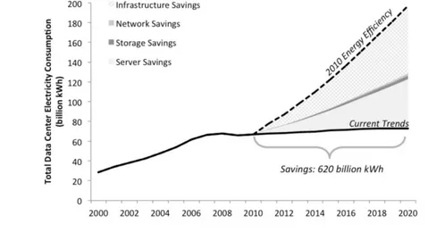
Therefore, the diminishing benefits from technology scaling, along with (i) the growing demand in mobile devices [8], especially in the IoT scenario, (ii) the battery technology's inability to provide sufficient low-cost and size solutions for these devices [9], and (iii) the contemporary growth in amounts of data processed by computing platforms from mobile devices to data centers and the consequent increase of energy consumption (see Figure 1.2) [10], have motivated researchers to look at new solutions for energy-efficient computing systems, while also keeping high performance.
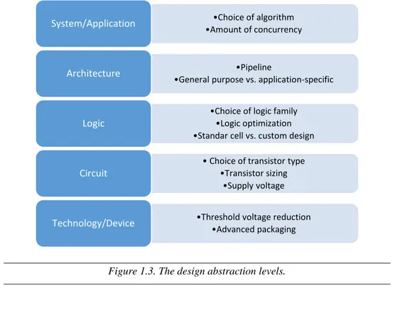
Overall, the design optimization process aimed at achieving a better energy/performance trade-off can occur at various abstraction levels [9], from the device- up to the system-level, as shown in Figure 1.3. The designer can then implement several solutions at different levels. This must be done taking into account that each level typically depends on each others, i.e. a propagation flow exists among design levels. In particular, the requirements/specifications usually propagate from the top to the bottom, whereas the restrictions propagate from the bottom to the top [11].
Figure 1.2. Past and projected growth rate of total US data center energy use from
1.2 Performance and power/energy metrics
Performance and power/energy consumption are the main figures-of-merit (FOMs) or quality metrics in VLSI design, along with the cost, the functionality and the robustness [9], [12], [13]. It is worth pointing out that which one of these FOMs is most important depends on the specific application requirements. For instance, the speed is typically the most crucial property in computing servers. On the contrary, for mobile applications such as cell phones, the energy consumption becomes the most prominent FOM [12]. However, the designer usually have to efficiently trade these two FOMs to ensure good performance, while also keeping energy consumption low. For this reason, it is useful to properly define these metrics and how to quantify them [13].
Figure 1.3. The design abstraction levels.
•Choice of algorithm •Amount of concurrency System/Application
•Pipeline
•General purpose vs. application-specific Architecture
•Choice of logic family •Logic optimization •Standar cell vs. custom design Logic
• Choice of transistor type •Transistor sizing
•Supply voltage Circuit
•Threshold voltage reduction •Advanced packaging Technology/Device
From a system designer perspective, the performance defines the computational load that a digital system can manage. For instance, a microprocessor is often characterized by the number of instructions it can execute per second. This performance metric depends both on the architecture (e.g., the number of instructions the circuit can execute in parallel) and the specific design style of the circuit [12]. When focusing on the circuit design, performance is typically expressed by the duration of the clock period or its frequency. The minimum value of the clock period for a given design is determined by a series of factors, such as the propagation time of the signals through the logic, the time it takes to get data in and out of the registers, and the delay time related to the clock arrival. Generally, the propagation delay (tp) of a logic gate represents the delay of a signal
when passing through that gate. It is typically measured between the 50% transition points of the input and output signals [12]. Because a gate often exhibits different responses for rising and falling input signals, two different delay times has to be defined: the tpLH related to a low (L) to high (H) output
transition, and the tpHL related to an H→L output transition. The propagation
delay is then defined as the average of these two values, as given by [12]
2
pLH pHL
p
t t
t = + (1.1)
In general, the transient response of a gate to an input change is mainly dominated by its output capacitance, although it also depends on the strength (i.e. the on-resistance) of its transistors [12]. Higher performance can be then achieved by keeping the output capacitance small or by decreasing the on-resistance of the transistors. Therefore, tp is strictly related to the
transistor technology and the circuit topology. However, it can depend upon other factors such as the slopes of the input and output signals. In this regard, it is necessary to introduce the rise (tr) and fall (tf) times, which are metrics
used to determine how fast a signal transits between two different levels. Generally, tr and tf are defined between the 10% and 90% points of the
signal. In a digital circuit, they are mainly determined by the strength of the driving gates, and the load presented at nodes, which sums the contributions of the connecting gates (fan-out) and the wiring parasitics [12].
The power consumption of a VLSI design determines how much energy is consumed per operation, and hence how much heat the circuit dissipates. This strongly influences several critical design choices, such as the power-supply capacity, the battery lifetime, power-supply-line sizing, packaging, cooling requirements, etc. [9], [12]. Therefore, power dissipation is a crucial property that also affects feasibility, cost, and reliability of a design. In the context of high-performance computing platforms, power consumption limits determine the number of transistors/circuits that can be integrated within a single chip, and how fast they can switch. Due to the increasing demand of mobile devices and distributed computing, power/energy limitations impose severe restrictions on the number of computations that can be performed given a minimum time between battery recharges [12]. Depending upon the design issues, different power dissipation metrics must be considered. For instance, the peak power (Ppeak) is crucial for supply-line
sizing, while the average power dissipation (Pav) is important when dealing
with cooling or battery requirements [12]. Ppeak and Pav are defined as
follows
( )
( )
( )
0 0 1 max , T DD T peak peak DD av DD V P i V p t P p t dt i t dt T T = = =
=
(1.2)where p(t) is the instantaneous power, T is the clock period, iDD is the current
drawn from the supply voltage over the interval [0,T], and ipeak is the
Typically, power/energy consumption can be decomposed into static and dynamic components. The latter occurs only during switching transitions, owing to the charging/discharging of capacitances and temporary short-circuit current paths between the supply rails. Therefore, it is proportional to the switching frequency, i.e. the higher the number of switching events, the higher the dynamic power consumption. On the other hand, the static consumption is present even when no switching events occur (e.g., during stand-by), owing to the static conductive paths between the supply rails or leakage currents [12]. Therefore, the three dominating components to the total power/energy consumption in a digital circuit are:
• static power (Pstat) and energy (Estat);
• dynamic power (Pdyn) and energy (Edyn) due to charging and
discharging of capacitances;
• short-circuit power (Psc) and energy (Esc) due to direct path currents
during switching. Accordingly, overall we have:
,
total stat dyn sc total stat dyn sc
P =P +P +P E =E +E +E (1.3)
The static (or steady-state) power and energy consumption of a circuit are defined by the following expressions, respectively
,
stat stat DD leak DD stat leak DD
P =I V =I V E =I V T (1.4)
where Istat is the current that flows between VDD and ground in absence of
switching activity. Ideally, the static current of a CMOS inverter is equal to zero, since the NMOS and PMOS devices are never on simultaneously in steady-state operation. In reality, the currents flowing through the reverse-biased diode junctions of the transistors located between the source or drain and the substrate, and the subthreshold conduction of the transitors (i.e. a MOSFET is never completely turn off) translate into a non-zero leakage
current (Ileak) and hence into a static power consumption [9], according to
(1.4).
As stated above, dynamic power consumption in a digital circuit is mainly associated to charging and discharging of capacitances occurring during switching events. Therefore, it strictly depends on the switching activity of the circuit. Considering a whole switching cycle (consisting of an L→H and an H→L transition) in a simple CMOS inverter, such dynamic power /energy consumption can be given by [12]
2 2
0 1,
dyn L DD dyn L DD
P =C V f → E =C V (1.5)
where CL is the load capacitance and f0→1 is the switching activity of the
circuit, i.e. the frequency of energy-consuming transitions corresponding to L→H output transitions for static CMOS. Considering that the switching activity in a complex circuit depends on several factors (e.g., the nature and the statistics of the input signals, the circuit topology, the function to be implemented, etc.), (1.5) is usually rewritten for a generic logic gate as follows [12]
2 2 2
0 1 ,
dyn L DD EFF DD dyn EFF DD
P =C V → f =C V f E =C V (1.6)
where f is the clock frequency, α0→1 is the activity factor, i.e. the probability
that a clock event results in a 0→1 event at the output of the gate, and CEFF
= α0→1CL is the effective capacitance, i.e. the average capacitance switched
every clock cycle. Note that technology advances typically result in higher values of switching activity as tp decreases, and also higher total capacitance
onto a chip due to the increased integration density [12].
During switching transitions, another contribution to the power dissipation of a digital circuit is due to the finite slope of the real input signals. Indeed, this causes direct (or short-circuit) current paths between VDD and ground
transistors are conducting simultaneously. Assuming that the resulting current spikes during this short period can be approximated as triangles and considering a CMOS inverter featuring symmetrical rising and falling responses, the short-circuit power dissipation/energy consumption can be given by [12]
0 1,
sc sc DD peak sc sc DD peak
P =t V I f → E =t V I (1.7)
where tsc is the time both devices are conducting and Ipeak represents the peak
of the short-circuit current during tsc, which strongly depends on the ratio
between input and output slopes [9]. It is worth pointing out that the short-circuit power consumption, as well as the dynamic power consumptions, depends on the switching activity.
Therefore, using (1.3)-(1.7), we can define the total power consumption of a simple CMOS inverter as the sum of its three components:
(
2)
0 1
total DD leak L DD sc DD leak
P =V I + C V +t V I f → (1.8) In the past, dynamic power consumption resulting from charging and discharging capacitances was dominant in typical CMOS circuits. More recently, with the introduction of deep sub-micron technologies and the consequent scaling of VDD and threshold voltage of transistors, leakage
currents have become more substantial to the point of being the primary source of power dissipation [9].
Performance and power consumption are strictly correlated in a digital circuit because the propagation delay is mainly determined by the speed at which a given amount of energy can be stored on the capacitors. The faster the energy transfer, i.e. the higher the power dissipation, the faster the circuit [12]. The product between power consumption and delay, namely power-delay product (PDP), is considered a quality measure for a digital circuit
[13]. It simply represents the average energy consumed by a circuit per switching event. However, the validity of the PDP as a quality metric in VLSI design is not fully recognized since, for instance, it can be arbitrarily reduced by decreasing the supply voltage. From this perspective, the optimum VDD in a specific circuit would be the lowest possible value that
still assures its functionality. But this occurs at the cost of lower performance [12]. For this reason, a more relevant metric is the energy-delay product (EDP), which allows combining performance and energy measurements. EDP is typically used in VLSI design as the ultimate quality metric to find the best energy/performance trade-off [12]. For instance, considering the impact of the supply voltage on the EDP, we can observe that higher VDD translates into lower delay but higher energy consumption,
while the opposite occurs for lower VDD. This means that an optimum
operation point (i.e., an optimum VDD) should exist. In general and more
specifically in the energy-constrained contexts such as the IoT, the design optimization is thus a trade-off process aimed at minimizing energy consumption for a given performance requirement or alternatively at maximizing performance for a given energy budget. As previously stated, this optimization process can occur at different design levels. As shown in Figure 1.4, it takes place in the energy-delay (E-D) plane with the aim of extending as much as possible the optimization space to facilitate the attainment of both delay and energy targets.
1.3 Purpose and organization of this work
As stated above, energy consumption represents a major design constraint in today computing systems. Moreover, the IoT paradigm has recently increased the demand for complex digital signal processing (DSP), multimedia systems and portable devices with flexible processing ability, high performance, small area, and low energy consumption [1]-[3]. In this regard, several solutions and strategies can be explored at different design abstraction levels. Among these, the design of variable-precision arithmetic units is a well-known approach to achieve more energy-efficient computing platforms [14]-[16]. This is particularly suitable for lossy multimedia applications (e.g., audio/video/image processing) where reducing the precision of arithmetic operations can be tolerated under the acceptable accuracy loss [16]. The design of multi-precision arithmetic units featuring an optimal energy/performance trade-off can be also facilitated by making appropriate choices at both circuit- and logic-level. To this purpose, a new logic family, namely Dual Mode Logic (DML), has been very recently
proposed with the aim of providing on-the-fly controllable switching at the gate level between static and dynamic operation modes [17]-[24]. This dual modularity typically allows wider energy/performance trade-off flexibility in the design and optimization of digital circuits [18].
In this context, the main purpose of this thesis work is to demonstrate the potential in combining the two aforementioned design strategies (i.e., multi-precision computing and DML design approach) in the design and optimization of arithmetic circuits (e.g., adders, multipliers, etc.). As a matter of fact, the flexibility inherently offered by DML is potentially very attractive to efficiently trade performance and energy consumption between the operations at different precisions in on-demand variable-precision digital circuits. In particular, as case study, this work mainly focuses on the design of a double-precision (8×8-bit or 16×16-bit) carry-save adder (CSA)-based array multiplier by exploiting the DML design approach [25]. For comparison purpose, the same benchmark has been also designed by using the standard static CMOS logic. All the circuits reported in this thesis have been implemented in a commercial 1.2V 65-nm low-power CMOS technology and characterized by means of circuit simulations in a commercial computer-aided circuit design tool, such as Cadence Virtuoso environment.
The rest of this thesis is structured as follows. Chapter 2 provides a brief overview of the most common CMOS logic design styles and it introduces the DML family. Chapter 3 first compares the DML design approach with the standard static CMOS style on a flexible circuit benchmark consisting of 10 levels of 11-stage NAND/NOR chains. Then, it describes in detail the proposed DML implementation of a double-precision (8×8-bit or 16×16-bit)
CSA-based multiplier, whose simulation results are provided and discussed over a wide range of process-voltage-temperature (PVT) variations in comparison with its static CMOS counterpart. Finally, Chapter 4 draws the main conclusions of this thesis work.
Chapter 2
2 Survey of Logic Families
Several circuit styles (or logic families) can be used for the implementation of a given logic function. Since each of these styles inherently holds its own advantages and drawbacks, the designer has to make an appropriate choice depending on the specific application and its requirements in terms of area, speed, energy consumption, robustness and reliability.
This chapter first provides a brief review of the most common design styles used to implement logic gates, blocks and digital circuits, such as the complementary (or standard) static CMOS and the dynamic CMOS. Both of these logic styles serve as basic building blocks for a novel and very promising logic design style, namely Dual Mode Logic (DML), whose
operating principle and main characteristics are then presented and discussed. The chapter ends by providing some guidelines to be used for the selection of the appropriate logic style when designing a digital circuits addressed to a specific application.
2.1 Complementary static CMOS logic
The most widely used logic family is the complementary static CMOS. Along with other circuit styles, such as ratioed logic, i.e. pseudo-NMOS and Differential Cascode Voltage Switch Logic (DCVSL) [26]-[28], and pass-transistor logic [29]-[31], such logic family belongs to the category of static (or non-clocked) circuits in which at every point in time each gate output is connected to either VDD or ground through a low-resistance path, thus
assuming at all times the value of the implemented logic function, except during the switching transitions. On the contrary, dynamic (or clocked) circuits are based on the temporary storage of signal values on the capacitance of high-impedance circuit nodes [12].
As shown in Figure 2.1, a generic standard static CMOS gate is based on the combination of two complementary networks: (i) the pull-up network (PUP) composed by PMOS devices, and (ii) the pull-down network (PDN) composed by NMOS devices. Note that all the inputs are distributed to both networks. The task accomplished by the PUN is to provide the connection between the output node and VDD anytime the output of the implemented
logic function has to be equal to "logic 1" on the basis of the inputs. Likewise, the PDN allows the connection between the output node and VSS
(typically the ground) when the output of the implemented logic function has to be "logic 0" on the basis of the inputs. Obviously, to properly
implement the given logic function, the two networks have to be built such that they are mutually exclusive, i.e. one and only one of the networks is active in steady state, thus always resulting into a low-impedance output node in steady state [12]. It is worth pointing that the complementary static CMOS gates are intrinsically inverting, thus requiring an additional inverter stage to implement non-inverting logic functions. Typically, NMOS and PMOS transistors are uniformly sized in complementary CMOS gates to have matching characteristics between PDN and PUN (i.e., same tpLH and tpHL), except for large fan-in gates for which a progressive transistor sizing
approach is usually adopted [12].
The advantages offered by the standard static CMOS design methodology are well known. Among these, we can mention the easiness of design, the robustness to noise, high scalability with technology and voltage, and until recent CMOS processes, almost no static power consumption. Conversely, the main drawback concerns the large amount of transistors required to implement a logic function (2N transistors for an N-input logic gate), which
translates into large input and output capacitances and hence reduced performance [32]. Moreover, as stated in Chapter 1, the advent of nanoscaled CMOS technologies has coincided with a dramatic increase of static leakage currents, thus leading to a no longer negligible contribution of the static power consumption.
2.2 Dynamic CMOS logic
As mentioned in the previous subsection, the complementary static CMOS requires 2N transistors to implement a logic gate with a fan-in of N. Different approaches were proposed to reduce the number of transistors required to implement a given logic function, including alternative static styles such as pseudo-NMOS and pass-transistor logics. For instance, the pseudo-NMOS logic style requires only N + 1 transistors to implement an
N-input logic gate, but at the expense of higher static power dissipation [12].
An alternative logic style, namely dynamic CMOS, was proposed to achieve similar results in terms of area occupation, while avoiding static power consumption and also ensuring higher performance with respect to static CMOS circuits.
The basic scheme of an n-type (or pre-charge) dynamic CMOS logic gate is shown in Figure 2.2. The operation of a dynamic gate is divided into two phases, i.e. the pre-charge phase and the evaluation phase, orchestrated by a clock signal (CLK). To this purpose, as shown in Figure 2.2, a clocked PMOS pre-charge transistor (Mp) and a clocked NMOS evaluation (footer)
transistor (Me) are used in the PUN and at the bottom of the PDN,
respectively, while the PDN is built as in the complementary static CMOS. In this way, during the pre-charge phase (i.e. when CLK = 0), the output
node is pre-charged to VDD through the PMOS transistor Mp, while the
NMOS transistor Me is off, thus disabling the PDN path and hence
preventing any static power consumption during this period. Conversely, during the evaluation phase (i.e. when CLK = 1), the precharge transistor
Mp is off, and the evaluation transistor Me is turned on. Thus, the output the
output node is conditionally discharged to ground depending on the inputs and the logic function implemented by the PDN. Whether the input values are such that the PDN is enabled, then a low-resistance path is established between the output node and ground to discharge the output node. On the contrary, if the inputs do not enable the PDN, the pre-charged value remains
stored on the capacitance of the output node. Accordingly, the gate inputs can lead at most to one output transition during each evaluation phase. It is worth noting that, when the PDN is disabled during the evaluation phase, the output is in the high-impedance state. This represents the main difference with respect to static CMOS circuits, where a low-resistance path
between the output and VDD or ground always exists. Therefore, in an n-type
dynamic CMOS gate the logic function is implemented by the PDN composed by NMOS devices. In a similar way, we can build a p-type (or discharge) dynamic CMOS gate by using a clocked NMOS pre-discharge transistor in place of the PDN and a clocked PMOS evaluation (header) transistor at the top of the PUN, which is built in that case as in the complementary static CMOS to implement the given logic function.
In general, when compared to the complementary static CMOS, the main advantages of the dynamic CMOS style are the smaller area occupation (N + 2 transistors versus 2N for an N-input logic gate) and the faster switching speeds owing to the reduced output capacitance (attributed to both the lower number of transistors per gate and the single-transistor load per fan-in) and the higher drive strength during the evaluation phase. Note also that n-type (p-type) dynamic CMOS gates can be constructed without the clocked footer (header) evaluation transistor, thus reducing both the area occupation (only N + 1 transistors for an N fan-in gate) and the clock load. Moreover, ideally, no static current path ever exists between VDD and ground. Instead,
the main drawback concerns the overall power dissipation, which can be significantly higher as compared to a static logic gate, mainly due to the clock power and the higher switching activity [12]. In addition, the dynamic CMOS logic style presents several other issues, including the charge leakage, the charge sharing, the capacitive coupling, and the clock feedthrough, which make this design approach particularly tricky [12]. These limitations are typically intensified with technology and voltage scaling, and under process and temperature variations.
Another important issue that complicates the design of dynamic CMOS circuits regards the cascading of dynamic gates of the same topology (i.e.
using the same clock signal) when implementing more complex logic structures. This problem is illustrated in Figure 2.3, where two n-type dynamic inverters are cascaded. During the precharge phase (i.e., CLK = 0), the outputs of both inverters are pre-charged to VDD. Assuming that the input
of the first inverter (In) makes a 0→1, as shown in Figure 2.3, on the rising edge of CLK, the output of the first inverter (Out1) starts to discharge. The
output of the second inverter (Out2) should remain in the pre-charged state
since its expected value is 1 due to the 1→0 transition of Out1 during the
evaluation phase. However, owing to the finite propagation delay for the input to discharge Out1 to ground, Out2 also starts to discharge. As a
consequence, there is a conducting path between Out2 and ground and hence
some charge is lost at Out2 as long as Out1 exceeds the threshold voltage of
the NMOS transistor of the second inverter. This conducting path is disabled only when Out1 reaches the NMOS threshold voltage, thus turning off the
transistor. This behavior leads Out2 to an intermediate voltage level, which
is not correct. Moreover, the correct voltage level on Out2 will not be
recovered since dynamic gates rely on capacitive storage and thus they do
not have static restoration. The resulting charge loss then produces reduced noise margins and potential malfunctioning [12].
This cascading issue occurs becasue the outputs of each gate (corresponding to the inputs of the next stages) are all pre-charged to VDD. This can cause
unwanted discharge at the beginning of the evaluation phase, as in Figure 2.3. A possibile solution to prevent this problem is setting all the inputs to 0 during the precharge phase. In tis way, all NMOS device in the PDN are in off after the precharge, thus avoiding inadvertent discharging of the storage capacitors during the evaluation. This means that correct operation is ensured as long as the inputs can only make a single 0→1 transition during the evaluation period. In this regard, two alternative dynamic design styles were proposed to implement this rule [12]:
• the Domino logic style;
• the NORA/np-CMOS logic style.
Domino logic style typically consists of cascading n-type dynamic logic blocks followed by a static inverter, as shown in Figure 2.4. This topology ensures that all inputs are set to 0 at the beginning of the evaluation phase, thus solving the aforementioned cascading issue. Indeed, during the pre-charge phase, the ouput of the n-type dynamic gates is pre-charged to VDD.
Accordingly, the output of the static inverters are set to 0. Then, during the evaluation phase, the dynamic gates conditionally discharge to ground its output node, and hence the ouput of the inverters makes a conditional 0→1 transition. In addition to solving the cascading issue, the additional static inverter ensures higher noise immunity due to the fact the fan-out of each gate is driven by a static inverter with a low-impedance path. Such buffer
stage also decreases the capacitance at the dynamic output node by separating internal and load capacitances [12]. However, Domino logic style
exhibits some limiting aspects mainly concerning the intrinsic non-inverting property, the high clock load owing to the need to use the footer evaluation transistor in the cascaded n-type logic blocks for preventing an extended pre-charge phase, and the reduced signal propagation time due to the presence of extra static inverters in the critical path [12].
An alternative solution to efficiently cascade dynamic logic blocks is represented by np-CMOS circuit style. As shown in Figure 2.5, it exploits the duality between n-type and p-type logic gates by alternatly cascading them, where the p-type logic gates are controlled by a flipped clock signal with respect to that of the n-type gates. In this way, n-type gates can directly drive p-type gates, and vice-versa. Furthermore, similar to Domino logic,
the ouput of n-type type) gates can be connected to another n-type (p-type) gate by inserting an extra static inverter (see Figure 2.5).
Therefore, np-CMOS logic guarantees high design flexibility, while also ensuring high performance and solving the cascading issue. The main
disadvanteges are the higher complexity in the clocking design, and the slower speed of p-type blocks, due to the lower drive strength of PMOS transistors, which typically leads to use wider PMOS transistors to equalize the propagation delays and hence to a greater area occupation.
2.3 Dual Mode Logic (DML)
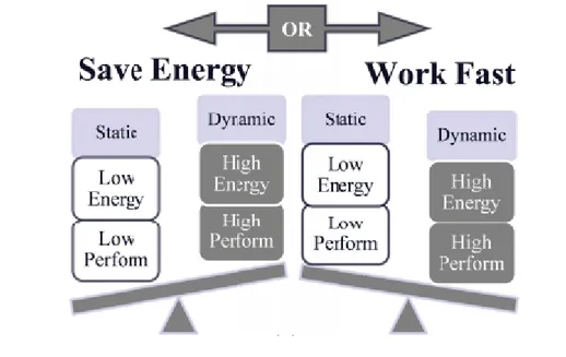
The DML family was recently introduced as a combination of complementary static and dynamic CMOS logic style with the aim of providing an alternative design methodology to the existing digital design techniques [17]-[19]. As a matter of fact, it allows on-the-fly controllable switching at the gate level between static and dynamic operation modes according to system requirements, input-driven control, and/or by designer considerations [18]. As shown in several previous works [17]-[24], such dual operation capability offered by the DML approach provides greater performance/energy trade-off flexibility in the design and optimization of digital circuits. As shown in Figure 2.6, the DML static mode typically assures energy saving at the expense of lower performance. Alternatively, the DML dynamic mode ensures higher performance at the cost of larger
energy consumption [18]. This means that the two DML functional modes
Figure 2.6. Performance/energy trade-off of DML gates in the two operation modes
exhibit different optimal curves in the energy-delay (E-D) space. Whereas the ability of on-the-fly controllable switching between the two operation modes theoretically allows the union of their optimal E-D curves, the DML design approach then provides an extended optimization space, thus making the attainment of E-D targets easier [22]. Moreover, it has been also shown that DML is fully functional, very robust and efficient for a wide range of supply voltage [18]-[21].
To implement the behavior described above, the structure of a basic DML gate relies on a conventional (complementary) static CMOS gate with an additional clocked pre-charge (or pre-discharge) transistor, which enables dynamic operation depending on a clock signal [20]. Similar to dynamic CMOS logic, DML gates can be implemented with or without a footer (or header) clocked evaluation transistor [22]. Figure 2.7 illustrates all the possible DML gate topologies: (a) footless Type-A with the pre-charge transistor and without the footer evaluation transistor, (b) headless Type-B with the pre-discharge transistor and without the header evaluation transistor, (c) footed Type-A with the pre-charge and the footer transistors, and (d) headed Type-B with the pre-discharge and the header transistors. The footer (or header) transistor is typically used to eliminate the ripple effect of the data advancing through the cascade and hence allowing faster pre-charge (pre-discharge) [18].
In all the topologies, during the static operation, the clocked pre-charge (or pre-discharge) transistor is always disabled, thus corresponding to CLK = 1 (0) in Type-A (Type-B) gates. As a result, the DML gates of both topologies
retain the functionality of the static core gate, except for the extra negligible parasitic capacitance due to the additional clocked transistor [22]. On the contrary, when the dynamic operation is required, the clock signal is enabled for toggling, thus providing two separate operating phases, i.e. pre-charge (or pre-discharge) and evaluation, as in dynamic CMOS logic. During the first phase, the output is charged to VDD in Type-A gates and discharged to
ground in Type-B gates, whereas during the evaluation phase the output is evaluated according to the values of gate inputs [18]. Typically, the DML gates exhibit a very robust operation in both static and dynamic modes under PVT variations and at low supply voltage [18]-[20]. In particular, as compared to the conventional dynamic CMOS logic, the DML gates operating in the dynamic mode ensure higher robustness by the intrinsic active self-restorer network, i.e. the PUN in Type-A topology and the PDN
Figure 2.7. Basic DML gate topologies: (a) footless Type-A, (b) headless Type-B, (c) footed Type-A, and (d) headed Type-B. Red traces represent the evaluation paths for
in Type-B topology, which allows sustaining glitches, charge leakage and charge sharing.
In general, when compared to its standard static CMOS counterpart, a DML circuit working in the static mode assures lower energy consumption with some performance degradation. Conversely, the dynamic mode can significantly improve the performance at the expense of higher energy consumption. The key factor to achieve the above behavior is the use of a proper transistor sizing methodology in the DML design, namely the unique sizing [18], [22]. It usually requires:
▪ the sizing of the evaluation networks in the static core (i.e. the PDN in Type-A gates and the PUN in Type-B gates, as shown in Figure 2.7) as in the standard static CMOS methodology, which typically consists of uniform transistor sizing to achieve a strength equivalent to that of one minimum-sized transistor;
▪ a downsizing of the active self-restore networks in the static core (i.e. the PUN in Type-A gates and the PDN in Type-B gates) by using minimum-sized transistors or anyway smaller devices with respect to the standard static CMOS design, which leads to a reduction of all capacitances in the DML gates, especially for the gate with large fan-in.
Accordingly, the downsizing of the self-restore networks is responsible for energy saving during the DML static operation mode at the expense of reduced performance due to their lower drive strength. At the same time, the low-resistive evaluation networks along with the capacitance reduction due to the downsized self-restore networks allows achieving fast operation in the DML dynamic mode and hence higher performance with respect to the static CMOS counterpart.
Note also that, when operating in the dynamic mode, the DML gates face the cascading issue as in the dynamic CMOS logic. Therefore, DML gates of the same topology can be connected through an extra static inverter as in the Domino logic style, otherwise the alternative solution consists of alternatly cascading Type-A and Type-B DML gates as in the np-CMOS logic style. Cascading DML gates of the same topology is also possibile without intermediate inverter stages when using footed (or headed) gates at each stage. Unfortunetely, this structure causes glitching. However, in this case, unlike the dynamic CMOS logic, the inherent self-restoring property of DML gates ensures the restoration of the logical value.
As stated above, the on-the-fly controllable switching between static and dynamic operation modes offered by DML gates has been efficiently exploited in the design and optimization of energy-efficient and high-performance digital circuits in several previous works [17]-[24]. For instance, the DML approach has been adopted to design carry-look-ahead [17] and carry-skip [18] adders by using a dynamic selection of critical paths according to the input vectors. The DML methodology has been also benchmarked on test chains of basic gates [19], [20]. A novel adder has been proposed in [21] by combining two independent design techniques, such as the DML and the dual-mode addition (DMADD), to achieve low energy, high performance and small area. The benefits of the DML have been also analyzed in [22], [23] on various meaningful benchmarks, such as multiplexers, decoders, comparators, arithmetic circuits. In addition, the combination of the operating characteristics of the DML along with the extended body bias capability offered by an ultra-thin box and body (UTBB) fully-depleted silicon-on- insulator (FD-SOI) technology has been recently evaluated on a NAND–NOR test chain and a 16-bit carry-skip adder [24].
2.4 Criteria for selecting the logic style
Since each logic style inherently features its own advantages and drawbacks, the choice of the most appropriate one is crucial when designing digital circuits. Obviously, such choice depends on the primary requirements in terms of speed, energy consumption and area occupation. Easiness of design, robustness and reliability also play a fundamental role in this task. It is worth pointing out that no single style allows all these specifications to be optimized at the same time. Even more, the selection criteria typically vary from application to application [12].
In general, the complementary static CMOS approach is the most widely used one thanks to the several advantages, mainly in terms of robustness to noise, and scalability with technology and supply voltage. All these features make the static design approach rather easy to be implemented and then particularly amenable to the use of design-automation tools at both logic and circuit level. Anyway, such benefits are achieved at the expense of reduced performance and high area occupation, especially in the design of complex circuits featuring large fan-in gates. The other static logic styles, such as pseudo-NMOS and pass-transistor logics, can represent a good alternative, but only for specific applications. Indeed, pseudo-NMOS allows the design of faster and simpler gates, but at the cost of reduced noise margins and higher static power dissipation. Instead, pass-transistor logic is usually attractive for the implementation of a reduced number of specific circuits, such as multiplexers and XOR-based logic blocks such as adders. On the other hand, dynamic CMOS logics allow designing fast and small digital circuits. However, this occurs at the cost of significantly higher power dissipation as compared to the static design styles and several other design
issues (such as the charge leakage, the charge sharing, the capacitive coupling, and the clock feedthrough) whose impact is typically intensified with technology and voltage scaling, and under process and temperature variations.
Depending upon the requirements of the specific application, a common approach used in the design and optimization of digital circuits is to combine different logical styles with the aim of exploiting the benefits of each single style. In this regard, thanks to its inherent dual operation capability, the DML style represents a powerful tool for digital designers. Figure 2.8 visually illustrates the DML operation space over the energy-performance plan considering that a DML circuit could operate in static or dynamic
Figure 2.8. DML operation space in the energy-performance plan.
DML Design Space (4) Unw ante d Re gion High Energy Low Energy High Performance Low Performance (4) Unw ante d Re gion (2) DML S tatic (1) DML D ynam ic (3) DML c ombi ned Mod e. Regio n(Pa rtial ly Di nam ic an d Parti ally Stat ic) Addi tiona l Con trol circu itry No Ad dition al Con trol circ uitry No Ad dition al Con trol circ uitry
mode, or even in a combined (mixed) mode, i.e. working partly statically and partly dynamically. As stated above, the control of the DML operation mode can be implemented in different ways, e.g. a priori on the basis of specific system requirements and/or designer considerations, or by implementing a smart input-driven control [18]. Obviously, such control can change the operation point of the DML circuit from one area to another one on the energy-performance plan, as shown in Figure 2.8, where region (4) is the undesired area corresponding to low performance and high energy consumption. Region (1) and (2) typically do not require additional control circuitry. Indeed, in these regions, a DML circuit works in one of the two possible operation modes. In region (1), the whole DML network operates in the dynamic mode by toggling clocked transistors in the charge (or pre-discharge) and evaluation phases. This allows high performance at the expense of high energy consumption. On the contrary, in region (2), the entire DML circuit operates in the static mode by disabling clocked charge (or pre-discharge) transistors, thus achieving low energy consumption, but reduced performance. Region (3) is located between the previous regions. In this region, the use of an additional control circuitry can potentially allow one to achieve better energy-performance trade-offs by efficiently combining the DML static and dynamic operation modes. For instance, a smart controller can select which logical paths have to operate in the static mode and which ones in the dynamic mode as a function of the input data [17], [18].
The DML design approach is particularly suitable for applications with a flexible workload, such as in multi-precision arithmetic circuits. The use of on-demand variable-precision circuits is typically addressed to lossy multimedia applications (e.g., audio/video/image processing) where in many cases a reduced precision of arithmetic operations can be tolerated under an acceptable accuracy loss for energy saving. The flexibility inherently
offered by the DML is then very attractive to efficiently trade performance and energy consumption between the operations at different precisions in multi-precision digital circuits. This can be achieved by properly tuning the DML operation mode according to the on-demand precision. More specifically, the DML design must operate in a mixed (or combined) mode, i.e. by employing the static and dynamic mode for lower- and higher-precision operations, respectively. Thereby, on one hand, the use of the dynamic mode in the DML circuit for higher-precision operations (which typically limit the performance of a multi-precision circuit) ensures higher clock frequency as compared to its static CMOS counterpart, obviously at the cost of higher energy consumption. On the other hand, the use of the DML static mode for lower-precision operations assures energy saving with respect to its static CMOS counterpart, thus potentially leading to counterbalance the energy penalty occurring at higher-precision operations. This DML-based design approach of multi-precision arithmetic circuits has been benchmarked in this thesis work on a double-precision (8×8-bit or 16×16-bit) multiplier, whose DML implementation is described in detail in the next chapter along with the comparative results with respect to its static CMOS counterpart.
Chapter 3
3 DML Evaluation and Its Application
for a Double-Precision Multiplier
This chapter evaluates the benefits of the DML design approach with respect to the standard static CMOS style. Such analysis is first performed on a flexible circuit benchmark consisting of 10 levels of 11-stage NAND/NOR chains. Then, as case study, the DML style is exploited for the design of a double-precision (8×8-bit or 16×16-bit) carry-save adder (CSA)-based array multiplier to efficiently trade performance and energy consumption between the operations at the two different precisions. In particular, this occurs when the proposed DML multiplier works in a mixed operation mode, i.e. by employing the DML static and dynamic mode for lower and higher precision operations, respectively.
For our particular case, all the circuits discussed in this chapter have been implemented by using low voltage threshold (LVT) transistors of a commercial 1.2V 65-nm low-power CMOS technology and characterized by means of circuit simulations in a commercial computer-aided circuit design tool, such as Cadence Virtuoso environment. However, we must also point out that in other works[24][43] it can observe that the benefits of Technolgy scales are consistent with the use of the DML logic, that is, the advantage in terms of Energy and performance is maintained with respect to the CMOS logic.
3.1 DML evaluation in a flexible circuit benchmark
As discussed in the previous chapter, the DML style allows on-the-fly switching at the gate level between static and dynamic operation modes [17]-[24]. In particular, the DML operation modes can be tuned at low-level of design granularity according to application-specific system requirements and/or designer considerations, or automatically by an input-driven control [18]. This means that DML static and dynamic operations can be enabled at the same time in different portions of a circuit, thus potentially allowing one to fully exploit the benefits of the two DML operation modes for better energy-performance trade-offs. Such powerful ability of the DML can be suitably highlighted on a flexible circuit benchmark consisting of 10 levels of 11-stage chains built by alternately cascading 2-bit DML Type-B headless NAND and Type-A footless NOR gates. This circuit can be considered as representative of a generic logic circuit. The schematics of the DML gates and the simulated test circuit are illustrated in Figures 3.1(a)-(c). Figure 3.1(c) also highlights the critical path of the circuit, which crosses all 10 levels as well as the whole bottom NAND/NOR chain. For the sake of
comparison, the same circuit has been implemented in standard static CMOS style by using the typical uniform transistor sizing approach [12], whereas the DML design exploits the unique sizing methodology already discussed in section 2.3. Accordingly, the transistors of the evaluation networks in the DML gates (i.e. the PDN and the PUN in Type-A footless NOR gates and Type-B headless NAND gates, respectively) have been sized as in the standard CMOS circuit, whereas those of the self-restore networks (i.e., the PUN and the PDN in Type-A footless NOR gates and Type-B headless NAND gates, respectively) have been downsized to save energy when using the DML static operation mode.
Figure 3.1. Schematic of (a) the 2-bit DML Type-A footless NOR gate, (b) the 2-bit DML Type-A footless NAND gate, and (c) the simulated NAND/NOR test bench
Figures 3.2(a)-(b) report simulation results in terms of delay and energy consumption obtained under supply voltage scaling (with VDD ranging from
the nominal voltage of 1.2 V down to 0.6 V) at the nominal process-temperature (PT) corner, i.e. (TT, 27°C), corresponding to typical N/PMOS transistors and operating temperature of 27°C. Reported data refer to both the standard CMOS and the DML implementations of the test chain. For the DML design, static (STAT), dynamic (DYN), and mixed (MIX) operation modes have been analyzed. The latter corresponds to the case when logic
Figure 3.2. (a) Delay and (b) energy results as a function of supply voltage (VDD) at the nominal process-temperature (PT) corner (TT, 27°C) for the simulated DML NAND/NOR test chain working in static (STAT), dynamic (DYN) and mixed (MIX) modes, and its static CMOS
gates belonging to the critical path operate in the high-performance dynamic mode, while the remaining gates operate in the low-energy static mode. As expected, the best performance are achieved when using dynamic operations along the critical path, i.e. for the DML circuit operating in DYN and MIX modes, while the DML design operating in STAT mode exhibits the lowest energy consumption, thanks to the downsizing of the self-restore networks in the DML gates, but at the cost of the worst performance. As shown in Figure 3.2, the MIX operation mode allows saving a significant amount of energy as compared to the case when the whole DML circuit operates in the dynamic mode, while keeping the same performance. This because, as stated above, in the MIX mode most of the DML circuit employs static operations to save energy, except for the DML gates along the critical path, which operate in the dynamic mode to ensure high performance. This can be also appreciated in Figure 3.3, where the simulation results are reported in the E-D plan along with the E-Delay-Points (ME-DPs) and the
Minimum-Figure 3.3. Energy-delay trade-off under VDD scaling at the nominal process-temperature (PT) corner (TT, 27°C) for the simulated DML NAND/NOR test chain working in static
Energy-Points (MEPs), obviously achieved at the highest VDD (1.2 V) and
the lowest VDD (0.6 V), respectively, in the considered VDD range. According
to previous results, the DML circuit working in the DYN and MIX modes exhibits the lowest MDP, whereas the lowest MEP is achieved when using the DML STAT mode. Figure 3.3 demonstrates that, when the two DML operation modes are properly mixed within the same architecture, the benefits offered by static and dynamic operations (i.e., energy saving and improved performance, respectively) can coexist, thus resulting into an extended optimization space in the E-D plan and hence better energy-performance trade-offs.
3.2 Case study: a double-precision DML carry-save multiplier
Multipliers play an important role in today's computing systems, especially for DSP and multimedia applications. Indeed, the design and implementation strategies of multipliers substantially contribute to the area, speed, and power consumption of computational intensive digital systems [33]-[38]. In general, a wide variety of computing arithmetic techniques and schemes can be used to implement a multiplication operation [12]. Among these, array multiplier is one of the most popular architectures for implementing parallel multiplication due to its regular layout and simple interconnects [36]. Array multipliers are typically implemented by directly mapping the manual multiplication into hardware, thus involving two steps: the generation of partial products (PPs) and their accumulation. The former consists of parallel logical AND operations between each bit of the multiplier and the multiplicand words. The latter is a multi-operand addition, which is implemented in an array of adder circuits to properly combine the generated PPs. Carry-save adders (CSAs) are widely used in array multipliers to accumulate the partial products [35]-[38]. Then, a final sum operation is needed for the generation of the multiplication result [12].
In this work, a CSA-based 2-stage pipelined multiplier for binary numbers has been designed by using the DML style. The circuit ensures on-demand double-precision (8×8-bit or 16×16-bit) operations at a constant clock frequency, which is typically limited by higher-precision operations in multi-precision digital circuits. As stated in the previous chapter, to efficiently exploit the dual operation capability inherently offered by the DML, the proposed DML multiplier works in a mixed (or combined) mode by tuning its operation mode according to the two different precisions, i.e.
by employing the static and dynamic mode for lower- and higher-precision operations, respectively.
3.2.1 Top-level architecture
Figure 3.4 illustrates the top-level architecture of the proposed 2-stage pipelined multiplier. The first stage consists of a CSA-based array for the generation and the accumulation of the PPs. The second stage produces the final multiplication result with a final sum operation performed by a carry-skip adder, whose structure is similar to that proposed in [24]. The circuit also includes five registers, i.e., two 16-bit registers for the multiplicand (A)
and the multiplier (B) inputs, respectively, one 32-bit register for the final
output (O), and two 31-bit intermediate (i.e., between the PP array and the final adder stage) pipeline registers.
To ensure the on-the-fly switching at the gate level between DML static and dynamic operation modes, a low-complexity extra clock control circuitry has been added in the proposed circuit. As shown in the left-upper part of Figure 3.4, this block receives as inputs the external clock signal (CLOCK) and a selection mode signal (MODE) to generate the internal clock signal (CLK) and its flipped version for DML gates. In this way, when MODE is low, it generates a high (low) CLK for Type-A (Type-B) DML gates to disable pre-charge (pre-discharge) clocked transistors, thus enabling the static operation mode. Conversely, when MODE is high, the dynamic operation mode is enabled by generating a CLK signal (and its flipped version) for properly toggling clocked transistors of DML gates in the pre-charge (or pre-dispre-charge) and evaluation phases.
As illustrated in Figure 3.4, a 16-stage clock buffer tree has been also introduced to generate 16 delayed clock signals (CLKi) (i.e., one for each
PP array row), with the aim of arranging an appropriate timing during dynamic operations. In particular, a proper design of the clock buffer tree is mandatory to ensure glitch-free and safe operations of the PP array at the two different precisions when the dynamic mode is enabled, especially at higher precision that involves longer signal propagation paths. A further control signal, namely PREC, has been then used as input for both the PP array and the final adder to set the on-demand operation precision. More specifically, an active low PREC signal translates into a higher-precision (i.e., 16×16-bit) multiplication, which requires a 32-bit final sum operation. Alternatively, a high PREC signal enables two contemporary 8×8-bit
![Figure 1.1. Real scaling trends over the years 1975-2010 obeying the Moore's law [5].](https://thumb-eu.123doks.com/thumbv2/123dokorg/2872745.9538/14.748.110.654.331.630/figure-real-scaling-trends-years-obeying-moore-law.webp)
![Figure 1.4. Energy-delay design space [9].](https://thumb-eu.123doks.com/thumbv2/123dokorg/2872745.9538/23.748.124.630.134.410/figure-energy-delay-design-space.webp)
![Figure 2.1. Basic scheme of an N-input standard static CMOS gate [12].](https://thumb-eu.123doks.com/thumbv2/123dokorg/2872745.9538/28.748.97.597.451.720/figure-basic-scheme-input-standard-static-cmos-gate.webp)
![Figure 2.2. Basic scheme of an N-input (n-type) dynamic CMOS gate [12].](https://thumb-eu.123doks.com/thumbv2/123dokorg/2872745.9538/30.748.101.626.440.751/figure-basic-scheme-input-type-dynamic-cmos-gate.webp)
![Figure 2.3. Cascading issue for n-type dynamic CMOS blocks [12].](https://thumb-eu.123doks.com/thumbv2/123dokorg/2872745.9538/32.748.94.623.390.618/figure-cascading-issue-n-type-dynamic-cmos-blocks.webp)
![Figure 2.4. Cascading of n-type gates in Domino CMOS logic style [12].](https://thumb-eu.123doks.com/thumbv2/123dokorg/2872745.9538/34.748.95.626.208.489/figure-cascading-type-gates-domino-cmos-logic-style.webp)
![Figure 2.5. Cascading of logic gates in np-CMOS logic style [12].](https://thumb-eu.123doks.com/thumbv2/123dokorg/2872745.9538/35.748.97.606.257.634/figure-cascading-logic-gates-np-cmos-logic-style.webp)