Towards the heterogeneous, real-time reconfigurable embedded system
Copyright c 2017 by
Acknowledgements
Good. The last page, last but not least. With these words I wrote my master thesis acknowledgments and I would like starting these in the same way, because this is indeed the most important page.
Many things have changed since I finished my master thesis, really a lot, maybe. . . too many. Perhaps, though everything happened led me to be what I am today (and I’m happy with it), it would have been better if something had remained as it was.
Despite difficulties such a long time passed so quickly and, for this reason I would like to thank those many people that helped me getting over them, making them less hard. I will thank everyone, trying not to forget anyone, and it will no longer matter who I will mention first, everyone has been important, none less than others.
I would like to thank Luca and Federico. Among Federico’s daily moaning and Luca’s past-new-year’s-eve-cotechino: we built a deep friendship. Between ups and downs, they always helped me and I know they will continue to support me. They were quite patient. . . I have to admit it! In addition to that, they taught me the importance of verticalising the work on horizontal lines of project which leads to greater efficiency that transversely affects all the working areas. Thanks to Federica and her daily attempts to make me date some of her friends (I would not say really successfully, so far).
Thanks to my new friends, Fabio, Cecche, Barsi, Peda, Chiarina, Orso, Leo, Ali, Caro, Cri, Fede, Pippo and Vale for dinners, holidays on the rocks and roast potatoes (which I just tasted!), for the mid-August pool-parties and barbecues and for beach-volley matches. Thanks for wine, laughs, but especially for raising my humor when I was down. With your positive attitude and your company you helped me moving forward, you made me smile even when I did not think I was able to. I hope I returned you at least part of the laughs you made me do.
Thanks to Ale, Tizi, Lore, Emi, Ste, Renzo and Leo for the nights spent together, the reunions around Europe, the homecomings, the laughs and friendship that we have been carrying out for almost 15 years. Despite we are in different times of our life, we always find ways to feed our friendship. I hope each of you, my friends, though sometimes feel drowning in the sea of problems, does not loose the strength to smile because “we do not have to wait for happiness to smile, but smile to make our own happiness”.
Thanks to Miche who has always been able to listen, always having the right words and being silent when it was needed. He is one of those rare people who actually knows how to help the others. Thank you.
Thanks to Benve, for the friendship and the evenings together that often helped me to see a little of light (and a good cocktail Martini) besides the dark moments.
If, as Aristotle said, ”the antidote against fifty enemies is a friend”, I am ready to face fifty thousand enemies.
Finally, I know I am contradicting myself but a special thank goes to my family, my Father, my Mother and my Sister, who always supported me, taught and encouraged me. Thanks to my Aunts Lidia, Rosa and Uncle Maurizio for the chats, the pleasant meetings, the warmth and the good wine. Eventually, I would like to thank my Grandmother for being the wisest, best person I have ever known.
Good. I reached the end of this experience and it is also your success if I have been able to get here. I wanted to write these acknowledgements because each of you, more or less consciously, has helped me to become what I am today.
Ringraziamenti
Bene. L’ultima pagina, last but not least. Ho cominciato cos`ı i ringraziamenti della mia tesi magistrale e comincer`o anche questi nello stesso modo, perch´e questa `e davvero la pagina pi `u importante.
Sono cambiate molte cose dall’ultima Discussione, davvero tante, forse. . . troppe. Forse, anche se gli avvenimenti mi hanno portato ad essere quel che sono oggi (e ne sono contento), sarebbe stato meglio se qualcosa fosse rimasto com’era.
Questi tre anni sono passati velocemente nonostante siano stati difficili. Devo ringraziare molte persone per averli resi meno pesanti. . . pi `u vivibili. Ringrazier`o tutti, cercando di non scordare nessuno, e non avr`a pi `u importanza chi menzioner`o per primo, ognuno `e stato importante, nessuno meno di altri.
Voglio ringraziare Luca e Federico con cui ho stretto una grande amicizia. Tra i giornalieri, mille lamenti di Federico ed i cotechini-del-capodanno-passato di Luca ab-biamo messo in piedi un bella amicizia. Tra alti e bassi, mi hanno sempre aiutato e sono convinto che continueranno a farlo. Sono stati piuttosto pazienti. . . devo ammetterlo! Inoltre, non meno importante, mi hanno insegnato che verticalizzare il lavoro sulle linee di progetto orizzontali porta ad avere un’efficienza maggiore che trasversalmente influisce su tutti gli ambiti aziendali. Grazie anche a Federica ed ai suoi continui tentativi di appiopparmi qualche amica (per ora, non direi proprio riusciti).
Grazie ai miei nuovi amici, Fabio, Cecche, Barsi, Peda, Chiarina, Orso, Leo, Ali, Caro, Cri, Fede, Pippo e Vale per le cene, le vacanze sugli scogli appuntiti e le patate arrosto (che ho solo assaggiato!), per i ferragosto in piscina e le braciate, le partite a beach-volley, per il vino e le risate, ma sopratutto per avermi aiutato e risollevato il morale quando non era giornata. Con il vostro spirito positivo e la vostra compagnia mi avete aiutato ad andare avanti, mi avete fatto sorridere anche quando non pensavo
di averne la capacit`a. Spero di avervi restituito almeno una parte delle risate che mi avete regalato.
Voglio ringraziare anche Ale, Tizi, Lore, Emi, Ste, Renzo e Leo per le uscite, le rimpatriate in giro per l’Europa, la compagnia, le risate e l’amicizia che portiamo avanti da quasi 15 anni. Pur essendo ognuno in momenti diversi della propria vita, troviamo sempre il modo di coltivare l’amicizia. Spero che ognuno di voi, amici miei, anche se sommerso dalle difficolt`a e dai problemi, non perda la capacit`a di sorridere perch´e “non bisogna aspettare di essere felici per sorridere, ma sorridere per essere felici”.
Grazie a Miche in cui trovo sempre una persona capace di ascoltare, che ha sempre le parole giuste e conosce il valore del silenzio. `E una delle poche persone che conosco che sappia aiutare l’altro. Grazie.
Grazie a Benve, per l’amicizia e le serate in compagnia che mi hanno spesso aiutato a vedere un po’ di luce (ed un buon cocktail Martini) a lato dei momenti bui.
Se, come diceva Aristotele, “l’antidoto contro cinquanta nemici `e un amico”, io sono pronto ad affrontarne cinquantamila.
Adesso, in effetti, mi contraddir`o, perch´e un grazie particolare va alla mia famiglia, Babbo, Mamma ed Ila, che mi hanno sempre supportato, insegnato ed incoraggiato. Grazie ai miei Zii Lidia, Rosa e Maurizio per le chiacchierate, i piacevoli confronti, la compagnia ed il buon vino e grazie a mia Nonna per essere la persona pi `u saggia e buona che conosca.
Bene. Siamo arrivati alla fine anche di questo capitolo ed ´e anche grazie a tutti voi che mi siete vicino che sono potuto arrivare fin qui. Questi ringraziamenti non sono dovuti, bens`ı voluti perch´e ognuno di voi, pi `u o meno consapevolmente, mi ha aiutato a diventare quello che sono oggi.
List of Publications
Enrico Rossi
1. F. Civerchia, E. Rossi, L. Maggiani , S. Bocchino, C. Salvadori and M. Petracca, “Lightweight Error Correction Technique in Industrial IEEE802.15.4 Networks”, 42nd Annual Conference of IEEE Industrial Electronics Society (IECON), Firenze, Italy, (2016)
2. A. Biondi, A. Balsini, M. Pagani, E. Rossi, M. Marinoni and G. Buttazzo, “A Framework for Supporting Real-Time Applications on Dynamic Reconfigurable FPGAs”, 37th IEEE Real-Time Systems Symposium (RTSS), Porto, Portugal, (2016) 3. F. Civerchia, S. Bocchino, C. Salvadori, E. Rossi, L. Maggiani and M. Petracca,
“Industrial internet of things monitoring solution for advanced predictive mainte-nance applications”, Journal of Industrial Information Integration, (2017)
4. E. Rossi, M. Damschen, L. Bauer, G. Buttazzo and J. Henkel, “Preemptive Partial Reconfiguration to Enable Real-Time Computing with FPGAs”, Transactions on Reconfigurable Technology and Systems, (2018)
Abstract
Towards the heterogeneous, real-time reconfigurable embedded system by
Enrico Rossi
To improve the computing performance in real-time applications, modern embedded platforms comprise hardware accelerators that speed up the tasks’ most compute-intensive parts. A recent trend in the design of real-time embedded systems is to integrate field-programmable gate arrays (FPGA) that are reconfigured with different accelerators at runtime, to cope with dynamic workloads that are subject to timing constraints, like in signal processing or computer vision applications.
One of the major limitations when dealing with partial FPGA reconfiguration in real-time systems is that the reconfiguration port can only perform one reconfiguration at a time: if a high-priority task issues a reconfiguration request while the reconfiguration port is already occupied by a lower-priority task, the high-priority task has to wait until the current reconfiguration is completed (a phenomenon known as priority inversion), unless the current reconfiguration is aborted (introducing unbounded delays in low-priority tasks, a phenomenon known as starvation).
Moreover, hardware accelerators reconfigured at runtime inside the FPGA usually require minimum interaction with the software side and perform massive computations on data which have to be read from the main memory or written to it. Therefore, In case of high-throughput hardware accelerators may happen that the communication medium shared between main memory and hardware and software sides is not able to accept more requests jeopardizing the functioning of the whole system. Furthermore, as the software can not control each bus transaction of an hardware accelerator,
mis-designed accelerators could perform illegal memory accesses corrupting the main memory.
This thesis shows how priority inversion and starvation can be solved by making the reconfiguration process preemptive, i.e., allowing it to be interrupted at any time and resumed at a later time without restarting it from scratch. Such a feature is crucial for the design of runtime reconfigurable real-time systems, but not yet available in today’s platforms. Furthermore, the trade-off of achieving a guaranteed bound on the reconfiguration delay for low-priority tasks and the maximum delay induced for high-priority tasks when preempting an ongoing reconfiguration has been identified and analyzed.
Besides, this work addresses the problems of memory protection and bus pre-dictability by showing a solution to prevent hardware accelerators from choking the communication bus or performing illegal memory accesses, making the communication more predictable and allowing for more precise analysis. A custom memory protection and budgeting unit (MPBU) has been developed for this purpose.
Experimental evaluation on the Xilinx Zynq-7000 platform have been realized for preemptive reconfiguration and MPBU. Results show that the proposed implementa-tion of preemptive reconfiguraimplementa-tion introduces a low runtime overhead, thus effectively solving priority inversion and starvation. Moreover, experimental results show that memory corruptionand bus chocking problems can be avoided and the communication over a shared bus can be made more predictable allowing to have less stringent timing constraints in the analysis.
Contents
List of Publications viii
Abstract ix
List of Figures xiv
List of Tables xvi
1 Introduction 1
1.1 The Heterogeneous, Real-Time Computing Era . . . 1
1.2 FPGAs and Dynamic Partial Reconfiguration . . . 3
1.3 Memory Protection and Bus Predictability . . . 6
2 Background 10 2.1 Field Programmable Gate Arrays . . . 10
Architecture . . . 11
Advantages and Disadvantages . . . 13
2.1.1 Softcores and System-on-Chip . . . 15
2.2 Advanced eXtensible Interface (AXI) . . . 18
2.2.1 AXI4 Interface . . . 19
AXI4 . . . 20
AXI4-Stream . . . 21
2.3 Dynamic Partial Reconfiguration . . . 21
2.3.1 Xilinx Bitstreams and Reconfiguration Port . . . 22
2.3.2 Decoding Partial Bitstreams . . . 25
Common Header . . . 27
Reconfigurable Slot Data Section . . . 27
Common Trailer . . . 27
3 Motivations and Contributions 29 3.1 Scheduling Problems . . . 31
4 Hardware and Software Design 37
4.1 Preemptive Partial Reconfiguration . . . 38
4.1.1 Finding Valid Resumption Points . . . 38
Simple Resumption Points . . . 40
Per-Frame Resumption Points within the Slot Data Section 41 Per-Frame Resumption Points within the Common Header 42 4.1.2 Software Interface for Preemptive Reconfiguration . . . 44
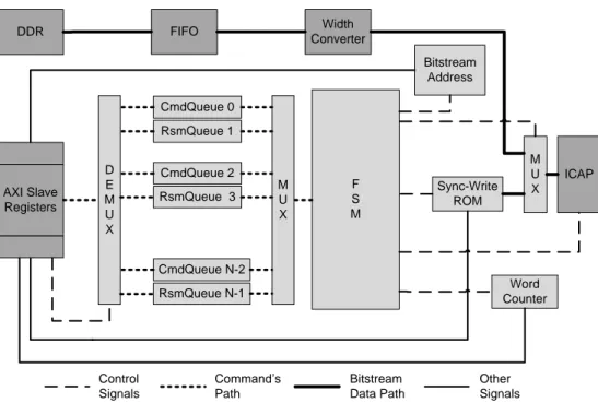
4.1.3 Preemptive Reconfiguration Controller . . . 46
Status Register . . . 52
Word Counter . . . 53
Bitstream Address . . . 53
Command’s Length Register . . . 53
Time-stamp Register . . . 53
Input Demux Control Register . . . 53
Command Register . . . 53
Current/Last-ran Command Register . . . 53
4.1.4 Hardware/Software Integration . . . 55
4.2 Memory Protection and Budgeting Unit . . . 56
4.2.1 Hardware Design and Functionalities . . . 58
Control Register . . . 61
Budget Register . . . 61
Budget Period Register . . . 62
Priority Register . . . 62
Memory Buffer Base Address Register . . . 62
Memory Buffer Offset Register . . . 62
Memory Buffer Mux Register . . . 62
Status Register . . . 62
Budget Counter Register . . . 63
4.2.2 Software Interface . . . 63
5 Analysis 65 5.1 Worst-Case Latency Analysis of Preemptive Reconfiguration . . . 65
5.1.1 Overhead for Preempting an Ongoing Reconfiguration . . . 66
5.1.2 Reconfiguration Delay of Preempted Reconfigurations . . . 69
Guaranteeing Minimum Reconfiguration Progress under Pre-emptions . . . 71
5.2 Worst-Case Analysis of the Budgeting Approach . . . 73
6 Experimental Evaluation 76 6.1 Evaluation of Preemptive Partial Reconfiguration . . . 77
6.1.1 Resource Utilization . . . 79
6.1.2 Maximum Observed Execution Time . . . 81
6.2 Evaluation of Memory Protection and Budgeting Unit . . . 84
Hardware System Description . . . 85
Resource Utilization . . . 86
Software Description . . . 86
6.2.1 Evaluation’s Results . . . 89
Baseline Performance Experiments . . . 89
Reservation Experiments . . . 90
7 Conclusions 94
List of Figures
1.1 Trend of reconfiguration throughput. . . 6
2.1 Generalized example of an FPGA architecture. . . 12
2.2 AXI channel architecture. . . 21
2.3 Sequence of operation performed in a partial bitstream. . . 23
2.4 Bitstream’s packet types. . . 24
2.5 Structure of a partial bitstream. . . 26
3.1 Scheduling problems in a multi-tasking system with non-preemptive resources. . . 32
3.2 Multi-master configuration of a communication bus . . . 34
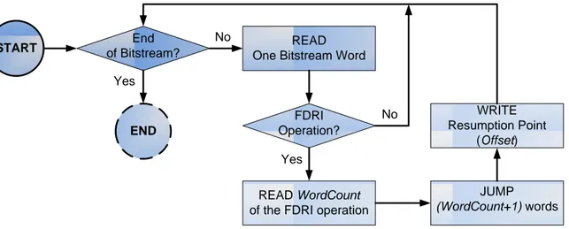
4.1 Position of Simple resumption points and Per-Frame resumption points. 39 4.2 Algorithm to find Simple resumption points. . . 40
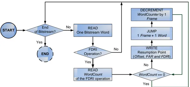
4.3 Algorithm to find Per-Frame resumption points. . . 42
4.4 Detailed structure of Data Chunk #0. . . 43
4.5 Block diagram of the custom Reconfiguration Controller . . . 47
4.6 Command’s format for the Reconfiguration Controller. . . 49
4.7 Data structure for two bitstreams with three resumption points each . . 54
4.8 Command sequence to resume a reconfiguration from Trivial, Simple and Per-Frame resumption points. . . 56
4.9 Memory Protection and Budgeting Unit placement. . . 57
4.10 Memory Protection and Budgeting Unit interface organization. . . 58
4.11 Internal block diagram of the Memory Protection and Budgeting Unit. . 60
5.1 Worst-case Execution time to preempt a reconfiguration. . . 69
5.2 Reconfigurable delay plot. . . 72
5.3 Typical data communication chain. . . 74
6.1 Block design of the evaluation system for preemptive reconfiguration. . 78
6.2 Priority inversion experiment. . . 82
6.4 Preemption experiment. . . 83
6.5 Block design of the evaluation system for MPBUs. . . 87
6.6 Baseline bandwidth of hardware modules and AXI bus. . . 91
List of Tables
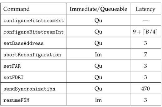
4.1 Reconfiguration Controller Commands. . . 51
4.2 Reconfiguration controller register map. . . 52
4.3 Memory Protection and Budgeting Unit register map. . . 61
6.1 Resource utilizaion of Reconfigurable Controller. . . 80
6.2 Maximum Observed Execution Time and Mean Executon Time compari-son. . . 84
6.3 Resource utilizaion of MPBU, MPBU controller and the evaluation desing. 88 6.4 Baseline values for tasks and memory thorughput. . . 90
Chapter 1
Introduction
1.1
The Heterogeneous, Real-Time Computing Era
Real-time systems are ubiquitous in our everyday life, e.g., in safety-critical domains such as automotive, avionics, or the rapidly growing domain of smart/autonomous machines (e.g., robotics or automated driving). In contrast to general-purpose com-puting systems, the correctness of a real-time system depends not only on the results of its computations, but also on the time at which outputs are produced. Delivering a result after a predetermined deadline may lead to malfunctions that can jeopardize the entire system. Therefore, for many safety-critical systems it is essential to guarantee that all time-sensitive computations are able to complete their execution within their deadlines.
To improve the performance of real-time systems, modern embedded platforms comprise hardware accelerators that speed up the tasks’ most compute-intensive parts.
Current computer architectures are evolving towards heterogeneous platforms con-sisting of hybrid computational devices that may include processors of different types and field programmable gate arrays (FPGAs). In particular, the reprogrammable
capa-bilities of FPGAs, their increasing capacity, and their suitability for signal processing have made them attractive in several application domains as alternatives to application specific integrated circuits (ASICs) [1]. Xilinx [2] provided an analysis of recent progress in field programmable logic, highlighting that FPGAs have become bigger (comprising several million gates and up to a million bits of on-chip memory), faster (allowing system clock rates up to 200 MHz and I/O speed of up to 800 Mbits/second), more versatile (featuring dedicated carry structures to support adders, accumulators and counters), and cheaper, in terms of cost per logic gate.
A recent trend in the design of real-time embedded systems is to integrate FPGAs that are reconfigured with different accelerators at runtime, to cope with dynamic workloads, like in signal processing or computer vision applications [3, 4, 5, 6, 7]. For instance, platforms like the Xilinx Zynq or Altera SoC combine general-purpose CPUs with an FPGA on a single chip to enable the development of application-specific accelerators that can run on the FPGA in parallel with the software executing on the CPU. Low-latency channels enable communication between accelerators and software.
In addition, the possibility of reconfiguring specific portions of the FPGA at speeds of 400 MB/s enables the adoption of runtime virtualization techniques to share the FPGA among multiple tasks in different time windows, so extending the number of functions that can be accelerated. Such a virtualization technique for the FPGA has been proven to be effective to achieve a significant speedup in real-time applications [8, 6]. Virtualization is generally realized using partial FPGA reconfiguration, where parts of the FPGA are reconfigured while the remaining configuration remains fully functional.
1.2
FPGAs and Dynamic Partial Reconfiguration
FPGAs are in demand for their inherent rapid-prototyping and reconfiguration capabilities. The reconfigurable computing [9] is an interesting alternative to ASICs and general-purpose processors for implementing embedded systems, since it offers the flexibility of software processors and the efficiency and throughput of hardware co-processors.
Modern FPGA chips allow dynamic partial reconfiguration capabilities, enabling the user to reconfigure a portion of the FPGA dynamically (at runtime), while the remainder of the device continues to operate [10]. This is especially valuable in mission-critical systems that cannot be disrupted while some subsystems are being redefined. In this context, mission-critical functions could continue to meet external interface re-quirements while other reconfiguration regions are reprogrammed to provide different functionality.
Partial reconfiguration is also useful in systems where multiple functions share the same FPGA resources. In such systems, one section of the FPGA continues to operate, while other sections are reconfigured to provide new functionality. Such an interesting capability opens a new scheduling dimension for applications running on heteroge-neous platforms. As in multitasking, where multiple applications share the processors by switching contexts between software processes, dynamic partial reconfiguration en-ables the possibility of interleaving multiple functions implemented as programmable logic on an FPGA recurrently shared by different processing components.
Partially reconfigurable FPGAs have many advantages over its non-reconfigurable counterparts. To list a few, a partially reconfigurable system can be re-synthesized after careful considerations resulting in the decrease of design time and consequently reducing the time-to-market. In the same way, parts of such systems can be altered
without having to shut down or even halt the system in its entirety, which undoubtedly enhances the system customizability and maintainability. Reconfigurable systems also allow the implementation of adaptive embedded systems incorporating self-optimization, self-organization of the system setup and self-adaptation to unpredictable changes in the environment [11]. In addition, the possibility of reconfiguring specific portions of the FPGA enables the adoption of runtime virtualization techniques to share the FPGA among multiple tasks in different time windows, so extending the number of functions that can be accelerated thus virtually extending the dimension of the FPGA. Such a virtualization technique for the FPGA has been proven to be effective to achieve a significant speedup in real-time applications [8, 6].
Although the partial reconfigurability of FPGAs offer new possibilities from the application perspectives, yet they pose many design challenges for today’s demanding applications. Of the few challenges currently being researched on in this field, some are related to reconfiguration time [12], dynamic allocation and placement of hardware tasks in reconfigurable regions [13], design and development of an on-line scheduler responsible for scheduling real-time tasks to reconfigurable regions [14] [15].
One of the major limitations when dealing with partial FPGA reconfiguration is that the reconfiguration port can only perform one reconfiguration at a time. This means that when multiple tasks issue simultaneous requests to reconfigure different portions of the FPGA fabric, such requests must be serialized according to a given scheduling algorithm. In current implementations, the reconfiguration port of the FPGA does not allow preemptions; that is, once a reconfiguration process is started, it can either be completed or aborted. In other words, if a high-priority task issues a reconfiguration request while the reconfiguration port is already occupied by a lower-priority task, the high-priority task has to wait until the current reconfiguration is completed, unless the current reconfiguration is aborted to be restarted later from the beginning (see
Chap-ter 3). Unfortunately, considering the relatively long reconfiguration delays of current platforms1, e.g., compared to context switching, both such solutions are not suitable for
real-time applications. In fact, while non-preemptive reconfigurations introduce long delays in high-priority tasks (a phenomenon known as priority inversion [16]), aborting them may introduce unbounded delays in low-priority tasks (a phenomenon known as starvation). Both problems can be avoided by making the reconfiguration process preemptive, allowing it to be interrupted at any time and resumed at a later time from the point of interruption. Such a feature is not yet available in today’s platforms.
Despite this limitation, there is a clear evolution trend showing that reconfiguration times are progressively decreasing. Liu et al. [17] designed a smart reconfiguration peripheral interface, based on the Xilinx internal configuration access port (ICAP) port [18], that is able to approach a throughput of 400 MB/s. Also, Duhem et al. [19] designed a fast reconfiguration interface by over-clocking the ICAP port up to 200 MHz, corresponding to a throughput of 800 MB/s. An overview of the trend of reconfiguration times (obtained by comparing the theoretical maximum throughput calculated from platforms’ datasheets) is shown in Figure 1.1, based on the study conducted by Pagani et al. [20]. For this reason, it is plausible to expect that such a trend will continue in the upcoming years, thus making dynamic partial reconfiguration a relevant direction to be explored.
Although reconfiguration times are not negligible, FPGAs allow hardware acceler-ation of a wide class of algorithms with a significant speedup factor [21, 22] over the corresponding sequential software implementation. In the case study analyzed in the work by Biondi et al. [6], a speedup factor up to 15x has been measured for an image
1For example: on the Xilinx Zynq-7010 platform which currently is the lower-end in terms of
reconfigurable resources, a maximum reconfiguration bandwidth of 400 MB/s is supported, however, reconfiguring 25% of the total resources still takes more than 2 milliseconds.
2000 2001 2002 2003 2004 2005 2006 2007 2008 2009 2010 2011 2012 2013 2014 2015 2016 100 300 500 700 900 Virtex II Virtex II Pro Virtex 4 Virtex 5 Virtex 6 Virtex 7 Virtex UltraScale Virtex UltraScale+ Year Theoretical Throughput (MB/s)
Figure 1.1: Trend of reconfiguration throughput.
processing filter implemented on the Zynq-7010 platform, which can reach a through-put of 145 MB/s for the dynamic partial reconfiguration, allowing to reconfigure an FPGA area containing about 25% of the total resources in less than 3 milliseconds.
1.3
Memory Protection and Bus Predictability
Other challenges of integrating partially reconfigurable FPGAs in real-time systems, reside in the system bus unpredictability. Real-time systems must be correct not only in the correctness and accuracy of calculations but also in the execution time. In particular, all the operation should be finished before deadlines [23].
Real-time systems can be classified into hard real-time systems and soft real-time systems according to the type of constraints applied on tasks. Tasks with a hard-deadline belongs to hard real-time systems where tasks are required to finish their execution strictly before the deadline or fatal mistakes would happen. On the other side, the violation of timing constraints in soft real-time system just leads to system
delay [24, 25].
Real-time tasks are required to fulfill two main requirements: timeliness of sponses which demand tasks to quickly respond a request, and predictability of re-sponse time which requires the task computation time to be computable [26].
Therefore, real-time systems which integrate FPGAs as accelerators have to comply with those requirements too. Software tasks could require hardware acceleration to speed-up their computation thus reducing the computation time and meeting their deadlines. In particular, systems integrating system-on-chips2(SoCs) or simple FPGAs
where custom accelerators are loaded at run-time inside the FPGA, may violate real-time requirements due to the unpredictability of the communication medium between hardware and software sides.
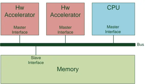
In fact, usually in those systems hardware accelerators require minimum interaction with the software side and perform massive computations on data which have to be read from the main memory or written to it. Moreover, as the main memory and the hardware and software sides connect on the same communication medium, a shared memoryapproach is the most common and straightforward method to provide communication between them: the software side shares with the hardware, part of the memory where both have full access.
In case of hardware accelerators that produce high traffic on the communication bus may happen that the bus is not able to accept more requests making other software tasks, which required hardware acceleration, miss their deadlines. Moreover, as the software can not control each bus transaction of an hardware accelerator, otherwise the computational speed-up will drastically decrease, mis-designed accelerators could perform illegal memory accesses corrupting the main memory.
2SoC FPGAs consist of processor, peripherals, and memory interfaces with the FPGA fabric using a
The same problems regarding the enhancement of application predictability and memory protection, have been addressed in pure software environments by the work of Cucinotta et al. [27]. They tackle the problem of providing Quality of Service guarantees to virtualized applications, focusing on computing and networking guarantees. They propose a mechanism for providing temporal isolation based on a CPU real time scheduling strategy allowing not only to have control over the individual virtual machine throughput, but also on the activation latency and response-time by which virtualized software components react to external events.
Moreover, the work by Liang et al. [26] shows a high-speed and time-predictable bus architecture called RTBus, where high-performance AXI protocol is employed. They developed a real-time bus arbitration algorithm to accurately calculate the bus access time for master devices.
This thesis presents the first solution for achieving preemptive partial reconfigu-ration of hardware accelerator’s reconfigureconfigu-ration onto an FPGA, preventing problems caused by a non-preemptable reconfiguration port shared among multiple tasks need-ing hardware acceleration. Moreover, it addresses the problems of memory protection and bus predictability by showing a solution to prevent hardware accelerators from choking the communication bus or performing illegal memory accesses, making the communication more predictable and allowing for more precise analysis.
Chapter 2 gives the required background on FPGAs. In particular, it present a general overview regarding FPGA’s architecture and features, focusing on the most commonly used communication bus (the advanced extensible interface - AXI) and deeply explaining the dynamic partial reconfiguration feature.
resource, i.e., the reconfiguration port, and a possible solution using preemptable partial reconfiguration. Furthermore, possible communication problems between hardware and software sides are presented. Eventually, the main contributions of this work are shown.
Chapter 4presents a real implementation of preemptive partial reconfiguration, focusing on finding valid resumption points for preempted reconfigurations inside Xilinx’s partial bitstreams. Moreover, the same chapter describes the implementation of a memory protection and bus budgeting unit that aims at avoiding illegal memory transactions and performs bus’ bandwidth budgeting for hardware accelerators. It also describes the software interface that has been realized to correctly use the developed hardware IPs for preemptive partial reconfiguration, memory protection and bus budgeting.
Furthermore, Chapter 5 determines worst-case bounds on the latency overhead that a higher-priority task experiences, when preempting a lower-priority task. It also determines an upper bound on the reconfiguration delay for reconfiguration requests from the lower-priority task for a given worst-case interval of reconfiguration pre-emptions and discuss under which circumstances preemption guarantees a minimum progress for these reconfigurations. Chapter 5 ends explaining what would be required to realize a worst-case analysis of a typical communication chain between CPU and FPGA and shows the limitations due to the lack of a detailed, public documentation of ARM and Xilinx IPs.
Eventually, Chapter 6 shows the performed evaluation of preemptive partial recon-figuration and bus’s bandwith budgeting on a real hardware platform integrating a Xilinx Zynq-7000 SoC.
Chapter 2
Background
In order to fully understand what has been done in this work, it is first necessary to present tools and technological solutions that have been used explaining their advantages and disadvantages. Therefore, this chapter introduces field-programmable gate arrays (FPGAs) (see Section 2.1) describing their general architecture and showing how nowadays systems can benefit from integrating an FPGA in their solutions.
Moreover, Section 2.2 describes the Advanced eXtensible Interface (AXI) which is the most common communication medium used by FPGAs.
Eventually, the chapter ends with the description of a particular feature of Xilinx’s FPGAs: dynamic partial reconfiguration. In particular, Section 2.3 introduce the par-tial reconfiguration feature describing its functioning and showing how the FPGA configuration file can be decoded for preemptive partial reconfiguration.
2.1
Field Programmable Gate Arrays
A field-programmable gate array (FPGA) is an integrated circuit designed to be configured by the user after manufacturing. Previously, as it was for application specific
integrated circuits (ASICs), FPGAs were configured using circuit diagrams but this method is increasingly rare as it is inconvenient and error prone for large designs. Nowadays the FPGA is generally configured using a hardware description language (HDL) that is a specialized computer language used to describe the structure and behavior of electronic circuits, and most commonly, digital logic circuits. HDLs were created to implement register-transfer level (RTL) abstraction, a model of the data flow and timing of a circuit [28], and enable a precise, formal description of an electronic circuit that allows for its automated analysis and simulation.
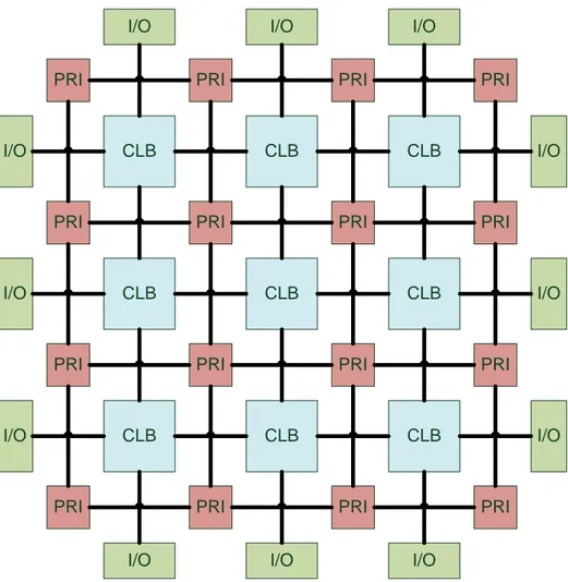
Architecture FPGAs have become one of the key digital circuit implementation media over the last decade. They are heterogeneous compute platforms that include RAMs, DSPs, look-up tables (LUTs) and an array of configurable logic blocks (CLBs) that are connected to each other through programmable routing interconnections (PRIs). A CLB is the basic component of an FPGA which provides the basic functionalities, logic and storage capabilities. Commercial vendors like Xilinx and Altera use LUT-based CLBs to provide basic resources and functionality. Figure 2.1 shows a generalized structure of an FPGA where CLBs are arranged in a two-dimensional grid and are interconnected by a PRI blocks. PRIs enable parallelism and pipelining of applications across the entire platform as all of these compute resources can be used simultaneously.
Contemporary FPGAs have large resources of logic gates and RAM blocks to im-plement complex digital computations. Some FPGAs have analog features in addition to digital functions. The most common analog feature is programmable slew rate on each output pin, allowing the user to set low rates on lightly loaded pins that would otherwise have unwanted oscillation, and to set higher rates on heavily loaded pins on high-speed channels that would otherwise run too slowly. Also common are quartz-crystal oscillators, on-chip resistance-capacitance oscillators, and phase-locked
CLB CLB CLB CLB CLB CLB CLB CLB CLB I/O I/O I/O I/O I/O I/O
I/O I/O I/O
I/O I/O I/O
PRI PRI PRI PRI PRI PRI PRI PRI PRI PRI PRI PRI PRI PRI PRI PRI
Figure 2.1: Generalized example of an FPGA architecture where configurable logic blocks (CLBs) are arranged in a two-dimensional grid and are interconnected by programmable routing interconnection (PRIs). PRIs also connect input/output (I/O) blocks with the internal configurable logic.
loops with embedded voltage-controlled oscillators used for clock generation and management and for high-speed communication interfaces.
A crucial part of FPGA’s creation lies in their architecture, which governs the nature of their programmable logic functionality and their programmable interconnect. Therefore, the architecture and especially the interconnect network has a dramatic effect on the quality of the final device’s speed performance, area efficiency, and power consumption.
The routing interconnect consists of programmable switches and wires which are used to build the required connection. As FPGAs claim to be a candidate to implement any type of digital circuits, their routing interconnect has to be very powerful and flexible in order to accommodate different circuits and their routing demands.
Different digital circuits require different routing networks but it is possible to define two types of routing: local routing and global routing. These routing methods connect logic blocks through the entire chip (global routing) or sections of it (local routing) with small propagation delay. Moreover, modern FPGA have specific routing resources to correctly route clock signals through the whole FPGA with the smallest possible propagation delay [29].
Advantages and Disadvantages The main advantage of FPGAs, i.e., flexibility, is also the major cause of its draw back. Flexible nature of FPGAs makes them significantly larger, slower, and more power consuming than their ASIC counterparts. These dis-advantages arise largely because of the programmable routing interconnect of FPGAs which comprises of almost 90% of total area of FPGAs.
Despite these disadvantages, FPGAs present a compelling alternative for digital system implementation due to their less time to market and low volume cost.
conventional ASIC implementations [30]:
• Easy upgrade. In contrast to traditional computer chips, FPGAs are completely configurable and functionalities can be upgraded at any time.
• Long-term maintenance. FPGAs enable independency from component manufac-turers and distributors, since FPGA chips can be reprogrammed to include new functionalities or upgrade the existing ones. Moreover, newer FPGAs support dynamic partial reconfiguration allowing to reconfigure only a portion of them while the rest of the logic continues to operate.
• Short time to market. The development of hardware prototypes is significantly shorter, since ideas and concepts can be verified in hardware without going through the long fabrication process of custom ASIC design. Moreover, the growing availability of high-level software tools decreases the learning curve with layers of abstraction and often offers valuable pre-built functions for advanced control and signal processing.
• Efficiency. Systems can be customized for the designated task.
• Cost. The silicon programmability removes fabrication costs and lead times for assembly. Because system requirements often change over time, the cost of making incremental changes to FPGA designs is negligible compared to the one of redesigning an ASIC.
• High performance. Taking advantage of hardware parallelism, FPGAs exceed the computing power of digital signal processors (DSPs) by accomplishing more operations per clock cycle. Also, controlling inputs and outputs at the hardware level provides faster response times and specialized functionality to closely match application requirements.
• Real-time applications. In contrast to software activities running in real-time operat-ing systems, FPGAs provide a more deterministic behavior, minimizoperat-ing reliability concerns with true parallel execution and deterministic dedicated hardware.
2.1.1
Softcores and System-on-Chip
Traditionally, FPGAs have been used only for application specific hardware designs. However, as their capacity and complexity increased with the advance in VSLI1
tech-nology, more complicated circuits and systems became possible. Vendors as Xilinx and Altera started providing general purpose softcores (also called softprocessors) solutions which enable to synthesize a programmable processor using the FPGA logic along with other IP blocks allowing users to develop more sophisticated systems.
General purpose softcores allows for quick prototyping of architectures where the advantages of both software and hardware design methodologies are mixed together. They offer designers tremendous flexibility during the design process, allowing full configuration of the processor to meet system’s constraints [31]. Moreover, a softcore-based design outperforms the traditional hardware-softcore-based design in terms of rapid prototyping, debugging capabilities and development time and cost while, compared to a purely software-based design is much more flexible for a hardware extension that replaces the critical kernel of the application.
It is well known that designs based on general purpose softcores lack in terms of performances and power consumption but the previously mentioned advantages, flexi-bility and scalaflexi-bility, allow it to be competitive against traditional methodologies [32]. In the early 1990s, the term ASIP has emerged denoting processors with an ap-plication specific instruction set 2 and as FPGAs provide resources to build custom
1Very Large Scale Integration
hardware modules, it is possible to build custom softcores, similar to ASIPs to fulfill application-specific requirements. Unfortunately, ASIP approach assumes that cus-tomizations are undertaken during design-time with little or no adaptation possible during run-time [34]. It is indeed hard or even impossible to predict the performance or other design criteria accurately during design time. Consequently, the more critical design decisions are fixed during design time, the less flexible an embedded processor can react to non predictable application behaviors [35].
Reconfigurable computing [36, 37, 38] i.e., FPGAs featuring dynamic partial re-configuration, may address this problem by enabling dynamic adaptivity through partial reconfiguration of the FPGA [35, 39, 40]. In fact, Bauer et al. in [34] combine the paradigms of extensible processor design and dynamic re-configuration in order to address dynamic changes of application’s characteristics due to switching to different operation modes or changes in design constraints (e.g., systems runs out of energy). Besides the approach of targeting full computational tasks in reconfigurable hard-ware [39] and the research for CPU-attached reconfigurable systems mainly focused on design-time predefined reconfiguration decisions. This is not suitable when com-putational requirements/constraints change during run time and are unpredictable during design time. Vassiliadis et al. present the Molen Processor which couples reconfigurable hardware to a base processor via a dual-port register file and an arbiter for shared memory [41]. In Vassiliadis et al. approach, the run-time reconfiguration is explicitly predetermined by additional instructions. The OneChip98 project [42] uses a Reconfigurable Functional Unit (RFU) that is coupled to the host processor and that obtains its speedup mainly from streaming applications. Eventually, Hauck et al. show that separating reconfigurable logic from the host processor, current custom computing systems suffer from a significant communication bottleneck. Therefore they designed Chimaera [43], a system that overcomes the communication bottleneck by integrating
reconfigurable logic into the host processor itself.
Besides general purpose and custom softcores, newer FPGAs exploit the System-on-Chip (SoC) technology which consists of the integration of multiple silicon die inside the same package. Those SoC FPGAs embed a more powerful, single or multi-core hard-processor which primarily differs from a softcore in the integration method: the hard-processor is directly integrated on a silicon die and connected to the FPGA die through an high-performance communication bridge.
Therefore, SoC FPGAs consist of a processor, peripherals, and memory interfaces with the FPGA fabric using a high-bandwidth interconnect backbone. It combines the performance and power savings of hard intellectual property with the flexibility of programmable logic. In particular, SoC FPGAs allow to reduce system power, cost, and board size by integrating discrete processors and digital signal processing (DSP) functions into a single FPGA and improving system performance via high-bandwidth interconnect between the processor and the programmable fabric.
Using a SoC FPGA and exploiting hardware acceleration allows meeting real-time constraints in applications where even high-end PCs usually fail. He et al. [44] present an FPGA-based SoC implementation of an efficient and robust face detection algorithm [45] that uses a cascaded Artificial Neural Network classification scheme based on AdaBoost-trained Haar features [46, 47]. They designed a face detection system which can detect faces at speeds of roughly two orders of magnitude (100×) higher than the corresponding software implementation running on a 2.4GHz CPU. Moreover, the work by Oetken et al. [48] proposes an FPGA-based SoC architecture with support for dynamic runtime reconfiguration in a smart camera case study. They implemented a reconfigurable design with support for free module placement and an enhanced memory access method for high-speed communication with an external memory.
2.2
Advanced eXtensible Interface (AXI)
Together with the introduction of soft-cores and SoCs and their increase in compu-tational power, the communication efficiency between cores and the FPGA has become a botleneck which limits the performance of systems based on those solutions [49][50]. Thanks to the flexibility of FPGAs, it is possible to implement with the internal logic a communication medium which allows the communication between soft/hard cores and hardware IPs integrated in the configurable fabric. Therefore, a standard bus architecture has been introduced in such devices in order to realize an efficient, flexible and powerful communication bus.
The Advanced eXtensible Interface (AXI) protocol is used by many SoCs and FPGAs today and is part of the ARM Advanced Microcontroller Bus Architecture (AMBA) specification [51]. The AMBA 4 AXI protocol builds on many benefits of the AMBA 3.0 AHB standard by greatly extending the performance and flexibility of the on-chip bus [52][53][54]. The AXI protocol provides the communication rules that different modules on a chip needs to abide by to communicate with each other. It is based on a handshake-like procedure before all transmissions and allows provides an effective medium for transfers of data between the existing components on the chip.
The main specifications of the protocol are summarized below:
• Before transmission of any control signals, addresses or data, both master and slave must extend their “hand” for a handshake via ready and valid signals.
• Separate phases exist for transmission of control signals, addresses and data. • Separate channels exist for transmission of control signals, addresses and data. • Burst type communication allows for continuous transfer of data.
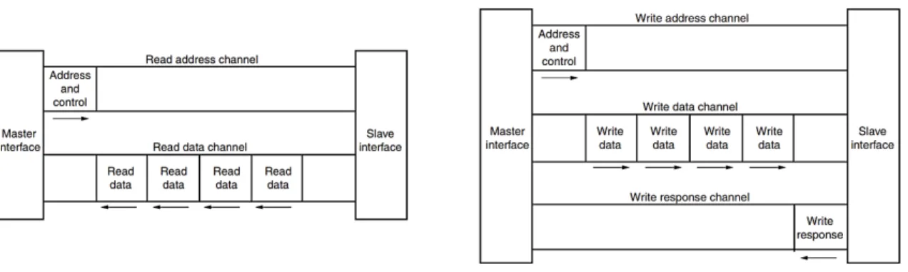
In particular, the interface works by establishing communication between master and slave devices. Between these two devices, five separate channels exist: Read Address, Write Address, Read Data, Write Data, and Write Response. Each channel has its own unique signals as well as similar signals existing among all five. The valid and ready signals exist for each channel as they allow for the handshake process to occur for each channel. For transmitting any signal (control signals, addresses or data) the relevant channel source provides an active valid signal and the same channel’s destination must provide an active ready signal. After both signals are active, transmission may occur on that channel. As stated above, the transmission of control signals, addresses or data, are done in separate phases, therefore an address must always be transferred before the handshake process can occur for the corresponding data transfer. In the case of writing information, the response channel is used at the completion of the data transfer.
Furthermore, there are additional options that the protocol provides which in-crease its complexity, such as burst transfer, quality of services (QoS) and protections. These options are simply extra signals existing on the different channels that allow for additional functionality.
2.2.1
AXI4 Interface
The AXI bus is especially prevalent in Xilinx’s Zynq devices, providing the inter-face between the processing system and programmable logic sections of the chip. In particular, Xilinx adopted the AXI4 version included in the AMBA 4.0 release. There are three types of AXI4 interfaces:
• AXI4 for high-performance memory-mapped requirements. It allows bursts of up to 256 data transfer cycles with just a single address phase.
• AXI4-Lite a subset of AXI4 for simple, low-throughput memory-mapped commu-nication. It is a single transaction memory mapped interface, has a small logic footprint and is a simple interface to work with.
• AXI4-Stream for high-speed streaming data. It removes the requirement for an address phase altogether and allows unlimited data burst size. AXI4-Stream inter-faces and transfers do not have address phases and are therefore not considered to be memory-mapped.
Xilinx adopted the Advanced eXtensible Interface (AXI) protocol for Intellectual Property (IP) interconnection and as a communication medium between cores and FPGA inside SoCs. AXI4 provides improvements and benefits to productivity, flexibility, and availability. Indeed improves productivity by standardizing on the AXI interface, enhances flexibility providing the right protocol for the specific application and increase availability by moving to an industry-standard.
AXI4 The AXI specifications describe an interface between a single AXI master and a single AXI slave, representing IP cores that exchange information with each other. Memory mapped AXI masters and slaves can be connected together using a structure called an Interconnect block. The Xilinx AXI Interconnect IP contains AXI-compliant master and slave interfaces, and can be used to route transactions between one or more AXI masters and slaves [51].
Both AXI4 and AXI4-Lite interfaces consist of five different channels: Read/Write Address Channel, Read/Write Data Channel and a Write Response Channel. Data can move in both directions between the master and slave simultaneously, and data transfer sizes can vary. As shown in Figure 2.2, AXI4 provides separate data and address connections for reads and writes, which allows simultaneous, bidirectional
Figure 2.2: AXI channel architecture. The organization of the read channel on the left side and of the write channel on right side.
data transfer. AXI4 requires a single address and then bursts up to 256 words of data. The AXI4 protocol describes a variety of options that allow AXI4-compliant systems to achieve very high data throughput. Some of these features, in addition to bursting, are: data upsizing and downsizing, multiple outstanding addresses, and out-of-order transaction processing.
AXI4-Stream The AXI4-Stream protocol defines a single channel for transmission of streaming data. The AXI4-Stream channel is modeled after the write data channel of the AXI4. Unlike AXI4, AXI4-Stream interfaces can burst an unlimited amount of data and transfers cannot be reordered.
2.3
Dynamic Partial Reconfiguration
Reconfiguring an FPGA is more complex than a simple transfer of the configuration data from main memory to the configuration memory of the FPGA. Especially when reconfiguring an FPGA partially, it needs to be ensured that the FPGA remains in a consistent state and the not-reconfigured parts remain functional all the time. A
partial bitstreamcontains all the information for the area that should be reconfigured, e.g., the address in the configuration memory that corresponds to the area of the FPGA where the design should be placed. The state of the FPGA is controlled by a finite state machine (FSM) that is part of the reconfiguration port. This FSM executes operationsthat are part of the bitstream besides the configuration data. Section 2.3.1 reports the information about the reconfiguration port and bitstreams that are openly available for Xilinx FPGAs [55] while Section 2.3.2 presents an approach to decode partial bitstreams and define a common structure that can be referred to when detailing preemptive reconfiguration. Such a structure is not openly available for Xiling FPGAs, hence it was part of this work to analyze the bitstream format in order to enable reconfiguration preemption and determine at what points reconfiguration of a bitstream can be preempted and resumed, as well as additional steps necessary to achieve this.
2.3.1
Xilinx Bitstreams and Reconfiguration Port
One of the contributions of this work, focuses on the reconfiguration port of Xilinx FPGAs, called Internal Configuration Access Port (ICAP). The information contained in the bitstreams for these FPGAs can be divided into two categories: operations executed by the reconfiguration port FSM and the actual configuration data that is transferred to the FPGA configuration memory. The smallest addressable segments of the con-figuration memory are called frames, and all operations act upon one or more frames. In Xilinx 7 Series FPGAs, each frame consists of 101 32-bit words [55]. The relevant operations for preemptive reconfiguration that are executed by the reconfiguration port FSM are summarized in the following.
Figure 2.3 shows the chronological sequence of the most relevant operations per-formed by partial bitstreams (a more detailed description can be found in Section 2.3.2).
Time Bus Width Auto-Detection Sync Word ID Code Check Shutdown Operation Set Control Registers Write Operation Config. Data Startup Operation Reset Operation Desync. Operation
Figure 2.3: Generic sequence of operations performed in a partial bitstream. White blocks are operations common to all partial bitstreams; gray blocks are specific oper-ations that depend both on the size and physical position of the reconfigurable area inside the FPGA and on the used FPGA device. These gray blocks constitute the largest part of the partial bitstream.
Partial bitstreams start with a Bus Width Auto-Detection operation that is used to auto-matically detect the word width that is sent to the reconfiguration port (1, 2 or 4 bytes are possible values). After that, the Synchronization Word initializes the reconfiguration port to accept configuration data, followed by the ID Code Check, which ensures that the bitstream target device matches the FPGA that is being reconfigured. The Shutdown Operationsafely shuts the area that is going to be reconfigured down and the Set Control Register Operationconfigures the available reconfiguration features. Write Operations transfer the actual configuration data, specifying the starting frame address and the amount of words (multiples of whole frames) to write.
After all configuration data has been loaded into the FPGA configuration memory, a Reset Operation is performed to initialize the logic inside the reconfigured region. Partial bitstreams end with a Startup Operation, where the device activates I/Os and the logic belonging to the reconfigured area, and a Desynchronization Operation that de-synchronizes the reconfiguration port (inverse to the Synchronization Word). After de-synchronization, the reconfiguration port ignores any following data on its inputs until the next synchronization.
• No-Operation. Decoded by the state machine without producing any actions. Since each operation is executed by the reconfiguration port FSM, each operation has a defined latency. This operation is used, when required, to introduce clock-cycles delays in order to wait for the completion of the running operation.
• Null Operation. This is a write operation that writes zeros to a specific FPGA register. Some operation as the Shutdown Operation and the Startup Operation need to be activated after being issued to the reconfiguration port FSM. The activation is done by a Null operation.
Each operation can be sent to the reconfiguration port in packets of two possible formats: ‘Type 1’ or ‘Type 2’. Type 1 packets are used when small amount of data words (to be read or written) are required by the operation. Type 2 packets are used to write long segments of data into the FPGA configuration memory. The address within the configuration memory needs to be supplied by a preceding Type 1 packet [55].
Header
Type Opcode Register Address Reserved Word Count [31:29] [28:27] [26:13] [12:11] [10:0]
Header
Type Opcode Word Count
[31:29] [28:27] [26:0]
Packet Type 1 Packet Type 2
Figure 2.4: The FPGA bitstream consists of two packet types: Type 1 and Type 2. The Type 1 packet is used for register reads and writes; the Type 2 packet, which must follow a Type 1 packet, is used to write long blocks. No address is presented here because it uses the previous Type 1 packet address.
As Figure 2.4 shows, both packet types have a Word Count field that contains the exact number of data words following the actual operation. It instructs the reconfigura-tion port FSM to directly write that amount of words to the configurareconfigura-tion registers or memory instead of decoding them.
Two FPGA-internal registers are central for the purpose of preemptive reconfigura-tion:
• Frame Address Register (FAR). It contains the address of the next frame in config-uration memory to be written.
• Frame Data Input Register (FDRI). It contains the number of data frames that have to be written to the FPGA configuration memory, starting from the frame address specified by the FAR register.
These registers are the reconfiguration state that needs to be restored when a reconfigu-ration is resumed.
The information summarized in this section has been gathered from openly-available Xilinx documentation [55], while the information in the following section were gathered by manually decoding partial and full bitstreams.
2.3.2
Decoding Partial Bitstreams
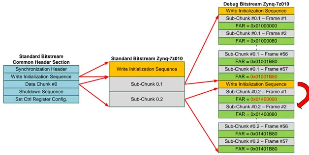
As mentioned in Section 2.3, there is no openly-documented structure of partial bitstreams provided by Xilinx. Such a structure is required for preemptive partial reconfiguration to determine points in the bitstream at which reconfiguration can safely be preempted and resumed. Therefore, a general structure for partial bitstreams is defined in the following, based on information gathered from decoding numerous bitstreams. There are two types of bitstreams that have been utilized to obtain the required information: standard bitstreams and debug bitstreams. Standard bitstreams configure multiple frames after a single write to the FAR and the FDRI registers, which increment automatically at the end of each frame. Debug bitstreams configure each frame individually, writing the FAR and the FDRI after each frame, and thus providing information about FPGA-specific configuration memory addressing.
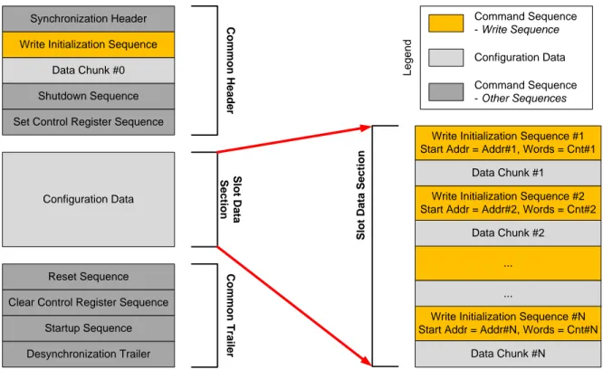
With information gathered by decoding both bitstream types, it has been possible to group operations in partial bitstreams into sequences that fulfill specific purposes. Each operation sequence can optionally contain configuration data organized in data chunks. Moreover, sequences in the bitstream have been grouped into sections (consisting of one or more sequences). Configuration data within a sequence of operations contains the description of the hardware that will be reconfigured inside the pre-defined reconfig-urable area, called reconfigreconfig-urable slot, inside the FPGA. The resulting general structure of sections for partial bitstreams in Xilinx 7 series FPGA is shown in Figure 2.5.
Synchronization Header
Write Initialization Sequence
Data Chunk #0
Shutdown Sequence
Set Control Register Sequence
Configuration Data
Reset Sequence
Clear Control Register Sequence
Startup Sequence C o m m o n H e a d e r S lo t D a ta S e c tio n C o m m o n T ra ile r ... ...
Write Initialization Sequence #N Start Addr = Addr#N, Words = Cnt#N
Data Chunk #N S lo t D a ta S e c ti o n
Write Initialization Sequence #1 Start Addr = Addr#1, Words = Cnt#1
Data Chunk #1 Write Initialization Sequence #2 Start Addr = Addr#2, Words = Cnt#2
Data Chunk #2 Command Sequence - Other Sequences Configuration Data Command Sequence - Write Sequence L e g e n d Desynchronization Trailer
Figure 2.5: Structure of a partial bitstream. The left hand side shows a partial bitstream where three main sections are identified: Common Header, Reconfigurable Slot Data Section, and Common Trailer. Darker sections are common to all partial bitstreams, while the Configuration Data section depends on the area that is reconfigured. The right hand side shows the structure of the Reconfigurable Slot Data Section.
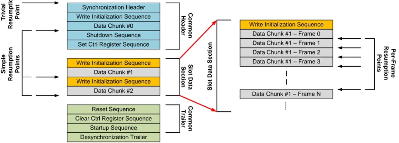
A partial bitstream can be structured into three main sections: Common Header, Reconfigurable Slot Data Section, and Common Trailer.
Common Header This first section is common to all partial bitstreams targeting the same FPGA and it is the only device-specific section. Its main function is to synchronize the reconfiguration port and prepare the device to receive the bitstream. It consists of the following four sequences: Synchronization Header, Write Initialization followed by its data chunk (which contains the data used to initialize special configurable blocks inside the FPGA), Shutdown and Set Control Register. These sequences are made of operations that initialize the reconfiguration port to receive data (Synchronization Word), set its bus width (Bus Width Auto-Detection), and perform the ID code check (ID Code Check). Furthermore, during the Write Initialization sequence, an FPGA-specific number of frames is sent to the configuration memory to configure particular resources called CFG CLB used to define which part of the FPGA itself will be reset or reconfigured [56]. This section ends with a Shutdown sequence, that safely disables the area that is going to be reconfigured, and a Set Control Register sequence which configures the FPGA device [55].
Reconfigurable Slot Data Section This section of the bitstream depends on the slot that is reconfigured. It contains the slot’s configuration data which describe the user-logic that will be written to the FPGA configuration memory. Configuration data is divided into an even number of data chunks consisting of numerous frames to be written into the configuration memory.
Common Trailer The last section is common to all partial bitstreams targeting the same FPGA. The function of this section is to reset the programmed logic and to
de-synchronize the reconfiguration port. Four main sequences can be identified: Reset, Clear Control Register, Startup and De-Synchronization Trailer. These sequences consist of operations used to initialize and activate the reconfigured logic and safely de-synchronize the reconfiguration port.
As explained in Section 2.3, partial bitstreams contain information for the area to be reconfigured and operations that control the reconfiguration FSM. Therefore, to enable preemptable reconfiguration, the knowledge of partial bitstream structures is essential, because a reconfiguration can be aborted at any time but can only be resumed from specific points in the bitstream. Section 4.1.1 explains which are the point in the bitstream where reconfigurations can be safely resumed.
This chapter presented all basic information necessary to fully understand this thesis. The following chapter explains the problems that have been considered as motivations of this work and the contribution to solve those problems.
Chapter 3
Motivations and Contributions
When exploiting FPGAs with Dynamic Partial Reconfiguration in real-time embedded systems, four main issues arise:
• provide worst-case response time bounds of computations consisting of software tasks and hardware accelerated functions;
• provide a method to avoid scheduling problems due to the use of a single, non-preemptive reconfiguration port;
• protect the system from malicious hardware accelerators that may possibly dis-rupt the whole application;
• enhance the bus predictability in order to provide more precise worst-case re-sponse time bounds.
Although several works have been done to analyze the timing behavior of real-time applications using FPGAs, most of them did not consider Dynamic Partial Reconfigura-tion capabilities at a job level. Only the work by Biondi et Al. [6] addresses the problem
of providing worst-case response time bounds and proposes a new computing frame-work for enabling a timing analysis of real-time activities that make use of hardware accelerators developed through programmable FPGAs with Dynamic Partial Recon-figuration capabilities. They use the developed framework to derive a response-time analysis and verify the schedulability of a real-time task set under given constraints and assumptions. Although the analysis is based on a generic model, the proposed framework has been conceived to account for several real-world constraints present on today’s platforms and has been practically validated on a real FPGA platform, showing that it can actually be supported by state-of-the-art technologies.
Furthermore, as explained in Chapter 1, Dynamic Partial Reconfiguration enables modifying parts of the logic configured on the FPGA while the remaining logic remains functional and it uses a single dedicated and non-preemptive reconfiguration port to write configuration data into the FPGA’s configuration memory. Therefore, only one reconfiguration at a time can be performed thus in a multi-tasking system where multiple tasks can request reconfigurations, the reconfiguration port is a contended resource.
Eventually, as hardware accelerators aim at unburdening the software side from compute-intensive tasks, there is the need to make hardware and software communicate in a fast, safe and reliable way.
Therefore, the purpose of this thesis is to provide the tools to make FPGAs integra-tion in real-time systems safer, avoiding malicious hardware accelerators to compro-mise the the whole application, more predictable, allowing for a more precise analysis of worst-case execution bounds, and more performing exploiting Dynamic Partial Reconfiguration and enabling reconfiguration preemptions.
3.1
Scheduling Problems
When a task issues a reconfiguration request (in this thesis is considered the model used and detailed in [6]), it self-suspends to wait for the reconfiguration to be completed, allowing the other tasks to execute on the CPU. Consider, for instance, a single-core system running two tasks, τ1 and τ2, with τ1 having higher priority than τ2. The
following three approaches can be adopted for managing reconfiguration requests:
a) Configure-to-completion: an active reconfiguration can not be preempted or aborted once started, but occupies the reconfiguration port until completed. This case is shown in Figure 3.1a, where τ2starts executing and takes control over the
reconfiguration port. When τ1 starts executing and requests a reconfiguration,
it must wait for τ2 to complete its reconfiguration, i.e., tasks are not executed
according to their priority order (priority inversion).
b) Abort: the reconfiguration process can not be suspended and resumed, but it can be aborted. Every time a reconfiguration was aborted, it needs to be restarted from the beginning. While this policy avoids priority inversion, it can lead to starvation of τ2, as shown in Figure 3.1b. τ2 starts executing and takes
control over the reconfiguration port, but its reconfiguration is aborted once τ1
requests a reconfiguration. When higher-priority reconfiguration requests abort
τ2’s reconfiguration frequently, then τ2suffers from starvation.
c) Preemptive reconfiguration: the reconfiguration requested by a task can be pre-empted in favor of another priority reconfiguration. When the higher-priority reconfiguration is completed, the suspended reconfiguration is resumed from the last valid point (where it is safe to resume the reconfiguration) already passed at the time it was suspended. As shown in Figure 3.1c, τ2starts executing
τ1 τ2 Reconfig. Interface 100% 100% Priority Inversion! 100%
SW Execution Reconfig. Request
Task Start/Stop Suspension HW Reconfig. HW Execution Hardware Execution
(a) Configure-to-completion leads to priority inver-sion: When an active reconfiguration can not be stopped, then τ1has to wait for τ2to complete its
reconfiguration even if τ1has a higher priority.
Reconfig. Interface 60% 100% τ2 Starves! 100% 40% ... Restart τ2 Reconfig.
SW Execution Reconfig. Request
Task Start/Stop Suspension HW Reconfig. Hardware Execution HW Execution τ1 τ2
(b) Abort leads to starvation: τ1 repeatedly
re-quests reconfigurations, aborting τ2’s
reconfigura-tion (that needs to be restarted from the beginning).
Reconfig.
Interface 60% 100% +30% 100% +10%
Resume τ2
SW Execution Reconfig. Request
Task Start/Stop Suspension HW Reconfig. HW Execution Hardware Execution τ1 τ2
(c) Preemptive reconfiguration solves priority inversion and starvation: Lower-priority reconfigurations can be preempted by a higher-priority task. The preempted reconfiguration can be resumed afterwards.
Figure 3.1: Multi-tasking systems can experience priority inversion and starvation problems due to a non-preemptive shared resource. Those problems are solved in this work for reconfigurations, by making the shared reconfiguration port preemptive.