IEEE TRANSACTIONS ON ELECTRON DEVICES, VOL. 54, NO. 4, APRIL 2007 879
Thermal Maps of GaAs P-HEMT: A Novel System Based on the Photocurrent Spectral Analysis
Andrea Reale, Aldo Di Carlo, Marco Peroni, Claudio Lanzieri, and S. Lavagna
Abstract—In this brief, we present a novel noninvasive method for spa-tially resolved thermal measurement of HEMT devices based on micropho-toconductance analysis. This approach is used to obtain the temperature distribution in the active regions of a GaAs P-HEMT. Through 1-D and 2-D thermal maps, we are able to measure the temperature inside each single channel, and owing to the improved spatial resolution of the developed technique, it is possible to observe the hottest region of the device which is placed at the drain side of the gate. Moreover, the resolution of the temperature measurements allows to define a local thermal resistance which is not uniform over the device due to the mutual heating between the channels.
Index Terms—Device heating, P-HEMT, spatially resolved photocon-ductance, thermal resistance.
I. INTRODUCTION
In transistor devices designed for high-power applications, the temperature of the active region is a very important parameter for the output power performance, since output current can be limited by channel heating effects [1]. Moreover, heating aspects are very impor-tant in terms of failure rate which, in devices like HEMTs, is mainly determined by the operating temperature of the channel [2]. Thermal management of high-power devices represents a critical aspect in device design. A detailed knowledge of self-heating effects and an accurate study of the power dissipation are thus needed, as well as the optimization of the geometrical layout and of the substrate mounting technology.
Several measurement techniques of device temperature are com-monly used: electrical dc method [3], IR techniques [4], liquid crystal techniques [5], Raman spectroscopy [6], cathodoluminescence [7], and photoluminescence spectroscopy [8]. Many of these methods do not allow the exact evaluation of the channel temperature, since some of these techniques (such as [4] and [5]) are able to measure only the surface temperature of the device, while some other techniques (such as [7] and [8]) may be affected by carrier diffusion phenomena that tend to smear out the knowledge of temperature distribution. Some others (such as [6]) are able to achieve an in-plane x−y accuracy slightly higher than our technique; however, this technique is based on the measurement of the optical phonon frequency of the GaN layer, and thus, it provides an averaged temperature information across the transversal growth direction due to the optical response of all the bulk GaN materials to the laser radiation. Recently, we have presented an efficient simple noninvasive method [9]–[11] of evaluating the actual channel temperature of FET devices based on the measurement of the photocurrent spectrum. The advantage of this method consists of the capability of measuring directly the temperature of the HEMT Manuscript received August 7, 2006; revised December 27, 2006. The review of this brief was arranged by Editor M. Anwar.
A. Reale and A. Di Carlo are with the Electronic Engineering De-partment, University of Rome Tor Vergata, 00133 Rome, Italy (e-mail: [email protected]; [email protected]).
M. Peroni, C. Lanzieri, and S. Lavagna are with the Department of GaAs, SELEX Sistemi Integrati, 00133 Rome, Italy (e-mail: [email protected]; [email protected]; [email protected]).
Color versions of one or more of the figures in this brief are available online at http://ieeexplore.ieee.org.
Digital Object Identifier 10.1109/TED.2007.891868
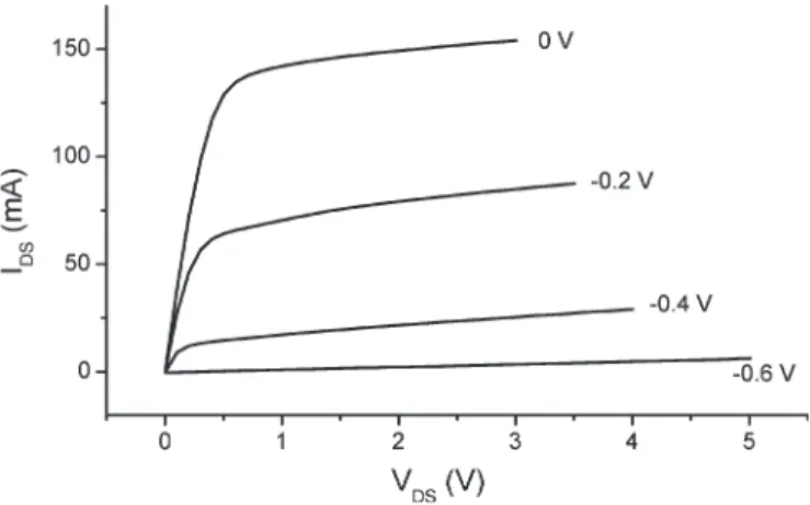
Fig. 1. I–V characteristics of the P-HEMT device. Pinch-off occurs at VGS=−0.6 V.
channel, even if this is well below the surface due to the fact that the collection efficiency of the channel is much higher. Thus, the photocurrent spectra are mainly related to the channel conditions. Moreover, carrier diffusion after photoexcitation does not affect the maximum achievable resolution.
In our previous works, we reported the photocurrent thermal mea-surements of HEMTs by uniform direct illumination [9]–[11]. In this brief, we extend the method to a spatially resolved photoconductance setup, where we focus the light through a single-mode fiber-optic system. The use of a fiber as exciting source allows us to estimate the temperature on an area of the order of fiber mode field diameter (less than 5 µm). The actual achievable resolution depends on the mode field diameter of the fiber we use (typically around 3 µm) and on the distance between the facet of the fiber and the surface of the device.
II. GaAs P-HEMT DEVICES
GaAs power P-HEMT devices have been fabricated by SELEX Sistemi Integrati S.p.A. on GaAs/AlGaAs/InGaAs heterostructures epitaxially grown on semi-insulating GaAs substrates. The manufac-turing process involves ohmic contact formation obtained by metal deposition of Au/Ge/Ni and subsequent rapid thermal annealing, ac-tive device isolation by ion implantation, gate recess wet etching, Schottky barrier metallization (Ti/Al) for gate contact formation, and surface passivation by plasma enhanced chemical vapour deposition silicon nitride. Finally, the substrate is thinned down to 100 µm, and via holes are realized through the backside to connect all the source pads. Measured devices have 10× 100 µm total gate periph-ery, drain-to-source distance of 5 µm, gate pitch of 30 µm, and gate length of 0.6 µm. The devices have been then placed in a 70MIL package and bonded by using silver epoxy. Current–voltage (I–V ) characteristics are shown in Fig. 1. The main RF parameters at 5 GHz are output power of 29.7± 0.1 dBm, linear gain of 14.6 ± 0.4 dB, and power-added efficiency of 56 ± 1% for VDS= 9 V,
IDS= 180 mA.
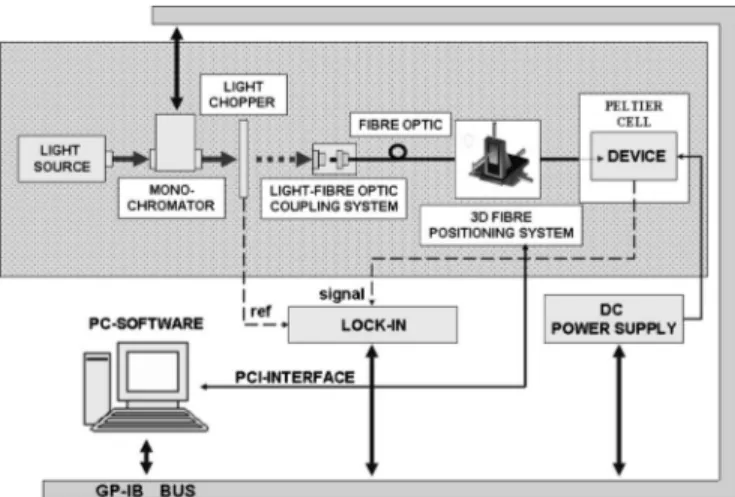
III. SPATIALLYRESOLVEDPHOTOCURRENTSETUP In order to obtain a spatially resolved photocurrent spectrum, we realized the setup shown in Fig. 2. The light emitted from a halogen lamp is dispersed by a monochromator, choppered and focused into a single-mode (cutoff wavelength of 370 nm, mode field diameter of 3.2 µm) fiber optic. The end of the fiber is mounted on a 3-D motorized 0018-9383/$25.00 © 2007 IEEE
880 IEEE TRANSACTIONS ON ELECTRON DEVICES, VOL. 54, NO. 4, APRIL 2007
Fig. 2. Spatially resolved photocurrent setup.
positioning system in order to focus the spot which comes from the fiber on the device-channel region.
The minimum increment along the x- and y-axes of each motor is 50 nm. The position of the light spot is monitored by optical mi-croscopy, which allows also the control of the fiber-channel distance. This fundamental parameter affects the effective spatial resolution, which can be greater or equal to the mode field diameter of the fiber.
The spatially resolved analysis requires a coherent detection via lock-in techniques of the photocurrent induced on the device. A voltage supply is used to bias the device during the power-dissipation measurements. A Peltier plate is used to fix the temperature (TP) of
the device carrier. The whole setup is remotely controlled by computer through the dedicated Labview virtual instrument.
IV. THERMALMAP OFGaAs P-HEMT
Thermal device performance can be evaluated in terms of the static thermal resistance obtained from the channel temperature as a function of the dissipated power.
In order to calculate the channel temperature, a thermal calibration is necessary. The device is biased with low dissipated-power condition (VGS= 0 V, VDS= 0.1 V, IDS= 40 mA). Then, the temperature of
the system is varied via Peltier cell. An increase of TPcauses the red
shift of photocurrent spectra due to the temperature dependence of the band gap.
We define λTHas the wavelength that corresponds to a particular
interpolated value of normalized photocurrent spectrum which repre-sents the edge of absorption spectrum (Fig. 3). In the following, we will consider as threshold wavelength the one which corresponds to the 70% of the maximum photocurrent. Other criteria can be used to define the adsorption edge, but we checked, and this does not change the final results (thermal maps). Calibration provides the relation between the temperature and the wavelength. In the temperature range considered in this brief (20 ◦C–100 ◦C), we found the following calibration expression: TCH [K] = (λTH− 363.86 [nm])/0.286 [nm/K], where
TCHis the temperature of the channel of the device. The accuracy of
the temperature measurement depends mainly on the uncertainty in the intensity of the photocurrent spectrum (the uncertainty in the spectral position is less than 1 Å) and on the slope of the spectrum at the 0.7 threshold. Each value of the photocurrent at any given wavelength is averaged through the use of the lock-in detection, with a root-mean-square error ∆I less than 2% of the maximum intensity detected in the whole photocurrent spectrum. The typical slope is α = 0.075 nm−1. The resulting uncertainty in the threshold wavelength is ∆λTH=
Fig. 3. Shift of the absorption edge of the photocurrent spectra of a GaAs P-HEMT occurring when the external temperature changes (VGS= 0 V,
VDS= 0.1 V, IDS= 40 mA).
Fig. 4. Linear profile of the temperature of nine channels at different dc power-dissipation conditions: 1) WDS= 256 mW with VGS= 0 V and
VDS= 1.8 V, and 2) WDS= 518 mW with VGS= 0 V and VDS= 3.5 V.
1/α· ∆I = 0.266 nm. This corresponds to a temperature uncertainty of 0.9◦C, according to the aforementioned calibration law.
It is possible to make a thermal calibration on a single point of the device, just focusing the spot at the desired position along one of the channels. We checked, however, that the calibration law is independent on the spot position, since it is only related to the intrinsic properties of the semiconductor material.
For each coordinate (x, y), a photocurrent spectrum is acquired. In this way, we get a λTH for every point, and through the
ther-mal calibration law, we determine the actual channel temperature TCH(x, y). A 1-D scan of the device is performed moving the light
spot along the channel direction. Fig. 4 shows the temperature distri-bution along the channels of the device at two different dc dissipated powers. Fig. 5 represents the details of the 1-D temperature distribution of two channels. These measurements have been performed with TP= 25◦C.
For each channel, the photocurrent spectra are collected over a region which results form the spatial convolution between the mode field diameter of the fiber and the real length of the channel. For this
IEEE TRANSACTIONS ON ELECTRON DEVICES, VOL. 54, NO. 4, APRIL 2007 881
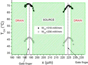
Fig. 5. Particular details of channel temperature in two adjacent channels: It can be observed that the zones between the gate and the drain have a major temperature.
Fig. 6. Two-dimensional temperature map of two GaAs P-HEMT channels (third and fourth of Fig. 5) at WDS= 256 mW with VGS= 0 V and
VDS= 1.8 V.
reason, the measurements shown in Figs. 4 and 5 slightly extend over the drain and source metallizations.
This technique allows us to profile the temperature variations be-tween the source and the drain. Fig. 5 clearly shows an asymme-try in the channel temperature, since the channel is hotter toward the gate–drain region. Such behavior is more evident at the higher dissipated power. This asymmetry within the device channel can be explained with the positioning of the hottest spot in correspondence with the higher electric field zone, located at the drain side of the gate junction, as well known from several reported simulations [12] and measured [13] data.
Two-dimensional temperature maps can be obtained in a similar way by scanning the surface of the HEMT in both x- and y-axes. At each scanning point, a full photocurrent spectrum is recorded, and local temperature is extracted via the calibration equation. Fig. 6 shows the interpolated data measured with constant steps along x- and y-directions (∆x = 0.5 µm and ∆y = 10 µm). The real time control of the software provides to exclude measurements at regions covered by metallization in order to reduce the measurement time.
Fig. 7. One-millimeter GaAs P-HEMT power device.
It can be seen that the temperature is greatest in the center of the channel and toward the drain region. Moreover, the heat distribution along the channel is not perfectly symmetrical. The lower region is hotter than the upper region which is in the proximity of via holes. The layout of the device is shown in Fig. 7.
V. THERMALRESISTANCE
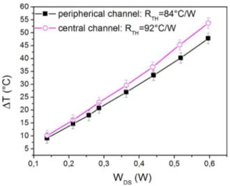
In the previous section, we have shown the thermal maps for a given dc bias. However, we can fix the measurement point and record the temperature variation as a function of the dc bias (i.e., the power dissipated in the device). These measurements have been performed for two reference channels (channels 5 and 10) with the light spot focused at the center of the channel. We found, in the bias range considered in this brief, a linear relation between the channel temperature and the dissipated power.
The usual concept of thermal resistance describes macroscopically the process of heating transfer, while the physical parameter that determines how, on a microscopic scale, the temperature distribution is related to the power dissipated in the device is the thermal con-ducibility. If one is interested to summarize the information of a local temperature distribution among the different channels of the device for a given dissipated power WDS, one can define a local thermal
resistance RTHfor any given active region of the device (not covered
by metallization) according to the following definition: RTH(x, y) =
∆TCH(x, y)
∆WDS
where (x, y) is any arbitrary position inside the channel, WDS= VDS·
IDS is the dc power dissipated within each channel, and ∆TCH=
TCH− TP. We observed that the thermal resistance changes from
channel to channel. In this case, a central channel (channel 5) has a thermal resistance RTH= 92 ◦C/W, while a peripherical one
(channel 10) presents RTH= 84◦C/W, as shown in Fig. 8. In this
way, we explain the temperature differences shown in Fig. 4, where the central channels are hotter than the peripherical ones. In this way, temperature disuniformities between the different channels of the device can be more easily ascribed to the effect of the geometrical layout and of the packaging of the device.
VI. CONCLUSION
We have presented a new technique for the spatially resolved mea-surement of the temperature in HEMT device through the micropho-tocurrent technique where the light is focused on the channel through
882 IEEE TRANSACTIONS ON ELECTRON DEVICES, VOL. 54, NO. 4, APRIL 2007
Fig. 8. Heating of channel 5 compared with channel 10. The central channel has an RTHgreater than the peripherical one.
a UV-single-mode fiber optic. This technique has been applied to mea-sure the 1-D and 2-D temperature distributions of GaAs P-HEMTs. We have been able to determine the temperature in each single point of the device channels and even to determine the asymmetry of temperature distribution between the source and the drain.
We have measured the thermal resistance in each single point of the device. The thermal resistance is a local property of the channel and depends on the device layout and package.
ACKNOWLEDGMENT
The authors would like to thank P. Mencherini and D. Angelilli for the assistance in the photocurrent measurements.
REFERENCES
[1] J. V. Dilorenzo and W. R. Wisseman, “GaAs power MESFET’s: De-sign, fabrication, and performance,” IEEE Trans. Microw. Theory Tech., vol. MTT-27, no. 5, pp. 367–378, May 1979.
[2] W.-C. Liu, K.-H. Yu, R.-C. Liu, K.-W. Lin, K.-P. Lin, C.-H. Yen, C.-C. Cheng, and K.-B. Thei, “Investigation of temperature-dependent characteristics of an n+-InGaAs/n-GaAs composite doped channel HFET,” IEEE Trans. Electron Devices, vol. 48, no. 12, pp. 2677–2683, Dec. 2001.
[3] D. B. Estreich, “A DC technique for determining GaAs MESFET thermal resistance,” IEEE Trans. Compon., Hybrids, Manuf. Technol., vol. 12, no. 4, pp. 675–679, Dec. 1989. [see also IEEE Trans. on Components, Packaging, and Manufacturing Technology, Part A, B, C].
[4] H. C. Huang, F. N. Sechi, and L. S. Napoli, “Thermal resistance of GaAs power FETs,” in Proc. 6th Biennial Cornell Elect. Eng. Conf., 1977, pp. 297–303.
[5] E. M. Fleuren, “A very sensitive, simple analysis technique using nemaic liquid crystals,” in Proc. 25th Int. Reliab. Phys. Symp., San Diego, CA, 1987, vol. 25, p. 369.
[6] M. Kuball, J. M. Hayes, M. J. Uren, I. Martin, J. C. H. Birbeck, R. S. Balmer, and B. T. Hughes, “Measurement of temperature in active high-power AlGaN/GaN HFETS using Raman spectroscopy,” IEEE Elec-tron Device Lett., vol. 23, no. 1, pp. 7–9, Jan. 2002.
[7] H. M. Kim, J. S. Yoon, S. H. Lee, J. E. Oh, W. S. Lee, K. I. Chun, K. W. Chung, H. W. Chung, and T. W. Kang, “New technique for the thermal resistance measurement of power field effect transistors using cathodoluminescence,” Jpn. J. Appl. Phys., vol. 39, no. 11A, pp. L1087– L1089, 2000.
[8] J. P. Landesman, B. Depret, A. Fily, J. Nagle, and P. Braun, “Local channel temperature measurements on pseudomorphic high electron mobility tran-sistors by photoluminescence spectroscopy,” Appl. Phys. Lett., vol. 72, no. 11, pp. 1338–1340, Mar. 1998.
[9] D. Savian, A. Di Carlo, R. Lugli, M. Peroni, C. Cetronio, C. Lanzieri, G. Meneghesso, and E. Zanoni, “Channel temperature measurement of
PHEMT by means of optical probes,” Electron. Lett., vol. 39, no. 2, pp. 247–248, Jan. 2003.
[10] P. Regoliosi, A. Di Carlo, A. Reale, P. Lugli, M. Peroni, C. Lanzieri, and A. Cetronio, “Thermal resistance measurement of GaAs MESFETs by means of photocurrent spectrum analysis and comparison with simu-lations,” Semicond. Sci. Technol., vol. 20, no. 2, pp. 135–139, Feb. 2005. [11] P. Regoliosi, A. Reale, A. Di Carlo, P. Romanini, M. Peroni, C. Lanzieri,
A. Angelici, M. Pirola, and G. Ghione, “Experimental validation of GaN HEMTs thermal management by using photocurrent measure-ments,” IEEE Trans. Electron Devices, vol. 53, no. 2, pp. 182–188, Feb. 2006.
[12] G. Ghione and C. U. Naldi, “High-resolution self-consistent ther-mal modelling of multi-gate power GaAs MESFETs,” in IEDM Tech. Dig., Dec. 3–6, 1989, pp. 147–150. Digital Object Identifier 10.1109/ IEDM.1989.74248.
[13] J. P. Landesman, E. Martin, and P. Braun, “Temperature distribution in power GaAs field effect transistors using spatially resolved photolumi-nescence mapping,” in Proc. 7th Int. Symp. Phys. and Failure Anal. Integr. Circuits, Jul. 5–9, 1999, pp. 185–190.
Concave-Suspended High-Q Solenoid Inductors With an RFIC-Compatible Bulk-Micromachining Technology
Lei Gu and Xinxin Li
Abstract—Presented in this brief is a concave-suspended solenoid induc-tor that can be post-CMOS integrated into a low-resistivity silicon sub-strate using a novel radio frequency integrated circuit (RFIC)-compatible micromachining technology. The three-mask processes include photoresist spray coating, XeF2gaseous etching and copper electroplating, etc. The
fabricated 11.5-turn inductor is measured with 2.96-nH inductance at 5.35 GHz, where the peak Q-factor is as high as about 45. Even with a compact layout (50% area occupation saved), the 8.5-turn inductor is still measured with 2.78 nH and peak Q of about 28 at 4.90 GHz. Both finite element simulation and shock testing results show that the suspended inductor is almost free of influence from environmental vi-bration and shock. Featuring high-Q performance and robust properties, the RFIC-compatible inductors are promising for high-performance RFIC applications.
Index Terms—Bulk micromachining, Q-factor, radio frequency inte-grated circuit (RFIC), solenoid inductors.
I. INTRODUCTION
On-chip integrated high-Q inductor is a key passive component in radio frequency integrated circuits (RFICs) such as voltage-controlled oscillators, low-noise amplifiers, filters, and impedance matching net-works [1]. The microinductors can be categorized into planar spiral inductors [2]–[10] and solenoid inductors [11]–[16]. Many efforts have been focused on 2-D spiral inductors due to the good integration ca-pability in standard silicon substrates. However, the aluminum planar spiral inductors generally exhibit a low Q-factor due to severe sub-strate loss and ohmic loss. In order to reduce the subsub-strate loss and the metal resistance, efforts have been made on fabricating high-Q spiral inductors, such as using porous silicon substrate [4], plastic substrate
Manuscript received July 12, 2006; revised December 13, 2006. This re-search is supported by Chinese 973 Project (2006CB300405). The review of this brief was arranged by Editor C.-Y. Lu.
The authors are with the State Key Laboratory of Transducer Technology, Shanghai Institute of Microsystem and Information Technology, Chinese Acad-emy of Sciences, Shanghai 200050, China, and they are also with the Graduate University of Chinese Academy of Sciences, Beijing 100049, China (e-mail: [email protected]).
Digital Object Identifier 10.1109/TED.2007.892362