87
Number
2021
Publication Year
2021-05-12T15:43:17Z
Acceptance in
OA@INAF
Advanced Techniques for VNA Characterization of
Millimetre-Wave Orthomode Transducers (OMTs)
Title
NAVARRINI, Alessandro; NESTI, Renzo
Authors
O.A. Cagliari
Affiliation of first
author
http://hdl.handle.net/20.500.12386/30957;
http://dx.doi.org/10.20371/INAF/TechRep/87
Handle
1
Advanced Techniques for VNA Characterization of
Millimetre-Wave Orthomode Transducers (OMTs)
1
Alessandro Navarrini and
2Renzo Nesti
1
INAF-Astronomical Observatory of Cagliari, Selargius, Italy 2
INAF-Astrophysical Observatory of Arcetri, Florence, Italy
Abstract
We report on advanced techniques for the characterization of millimeter-wave orthomode transducers (OMTs). These techniques include standard mm-wave frequency-domain VNA (Vector Network Analyser) measurement and time-domain methods, which can be applied to remove the effects of the waveguide transitions necessary to access the OMT ports and excite the desired modes. First, we present the main parameters of the OMT by defining its general S-matrix and discuss the different methods that allow characterizing the insertion loss, the reflection, the cross-polarization and the isolation of the device. Advantages and disadvantages of each method are presented and compared between them. We provide a list of waveguide components necessary in the various OMT test setups (adapters, loads, quarter-wave and longer waveguide sections, feed-horn, etc.). Different OMT configurations, with distinct orientation of the waveguide input and outputs are discussed. Alternative characterization methods of the OMT parameters are presented and the associated setups discussed.
Although the presented techniques refer to the characterization of a specific configuration of a W-band (3 mm wavelength) OMT, the described method can be applied to other OMT configurations and frequency ranges (from microwave to THz frequencies), therefore having a general validity.
Introduction
An Orthomode Transducer (OMT) is a passive device operating in a dual mode [1]: in receiver mode, it separates two orthogonal linearly polarized signals at its common input port to two independent physical ports at its output; in transmitter mode, it combines two independent signals at its two input ports into two separate polarizations at the common output port. In the two operating modes, input/output port/ports are exchanged. Here we focus on the receiver mode, being most of the discussion valid also in transmitting mode. The polarization separation is realized over a given frequency range. An OMT has three physical ports, but exhibits properties of a four-port device, because the input common port, usually a waveguide with a square or circular cross-section, provides two electrical ports that correspond to the independent orthogonal polarized signals. Various OMT designs exist. A selection of references that describe OMTs operating at millimetre and sub-millimeter wavelengths is given in [2]-[24].
Fig. 1. Schematic diagram of an OMT showing the common input with the two electrical ports, Port 1 and Port 2, associated respectively to VP and HP signals, as well as the two independent physical ports at the device outputs, associated to output port VP (Port 3) and output port HP (Port 4).
2
The schematic diagram of an OMT, a four-electrical-port device, is shown in Fig. 1. Electrical ports 1 and 2 are associated to the two orthogonally incident polarizations at the input of the device, a circular or square waveguide. They share the same physical port. Port 1 signal is defined here as the “Vertical Polarization” and is represented by a vertical E-field vector VP, while Port 2 signal is defined as the “Horizontal Polarization” and is represented by a horizontal E-field vector HP.
Ideal OMT and definition of OMT parameters
In an ideal OMT, the signal VP at Port 1 is fully coupled to the VP output port, Port 3, while the signal HP at Port 2 is fully coupled to the HP output port, Port 4. In addition, the VP and HP signals at the common ports, Port 1 and Port 2, are perfectly matched (no reflection). Similarly, the output ports VP and HP, respectively at Port 3 and Port 4, are perfectly matched. There should be zero coupling between the input VP signal (at Port 1) and the HP output port signal (Port 4) and between the input HP signal (at Port 2) and the output VP port signal (at Port3). Furthermore, when the OMT inputs at Port 1 and Port 2 are matched, the coupling between signals at Port 3 and Port 4 should be zero. The S-parameter matrix [25]-[27] of a four-port device is given in (1), while the one of an ideal OMT is given in (2):
𝑆 = [
𝑆
11𝑆
12𝑆
13𝑆
14𝑆
21𝑆
22𝑆
23𝑆
24𝑆
31𝑆
32𝑆
33𝑆
34𝑆
41𝑆
42𝑆
43𝑆
44] (1)
𝑆 = [
𝑆
11𝑆
12𝑆
13𝑆
14𝑆
21𝑆
22𝑆
23𝑆
24𝑆
31𝑆
32𝑆
33𝑆
34𝑆
41𝑆
42𝑆
43𝑆
44] = [
0
0
1 ∙ 𝑒
𝑖𝜃130
0
0
0
1 ∙ 𝑒
𝑖𝜃241 ∙ 𝑒
𝑖𝜃310
0
0
0
1 ∙ 𝑒
𝑖𝜃420
0
] (2)
In general, the elements Sij of the 4×4 matrix have frequency-dependent complex values, which in the
ideal OMT take the values indicated on the right side of eq. (2), where only the amplitudes of elements S31, S42, S13 and S24 are unitary (on a linear scale). The phases of each of the Sij are also indicated for
the non-zero elements (31, 42, 13, and 24).
An OMT is passive device that contains only reciprocal materials, and therefore has properties of a reciprocal network. A reciprocal network is one in which the transmission of a signal between any two ports does not depend on the direction of propagation, i.e. input and output ports are interchangeable. In S-parameter terms, this means Sij = Sji for any i≠j1, i.e. S12 = S21 , S13 = S31 , etc... A consequence of
this property is that any reciprocal network, including any OMT, has a symmetric S-parameter matrix, meaning that all values along the lower-left to upper-right diagonal of eq. (1) and (2) are equal. In particular, for an ideal OMT we have 31=13, 42=24.
The main parameters that characterize the performance of an OMT are the following: I. The Insertion Loss, IL, of the two polarization channels;
1 Most passive networks such as cables, attenuators, power dividers, and couplers are reciprocal. The
only case where a passive device is not reciprocal would be when it contains anisotropic materials, which have different electrical properties (such as relative dielectric constant) depending on the direction of signal propagation. One example of an anisotropic material is ferrite, which is used in circulators and isolators for the specific purpose of making these nonreciprocal devices. Transistors and other two-port active devices are typically nonreciprocal, since S12 ≠ S21 in most cases.
3
II. The Input Return Loss, IRL, of the two input polarization channels; III. The Output Return Loss, ORL;
IV. The Cross-Polarization, XP;
V. The Isolation, ISO, between the output ports.
The Insertion Losses, IL, are associated to the signal losses through the OMT from Port 1 to the corresponding output Port 3 (IL31), and from Port 2 to the corresponding Port 4 (IL42); they are defined
as follows:
𝐼𝐿31= −20 𝑙𝑜𝑔10|𝑆31| 𝑑𝐵 (3)
𝐼𝐿42= −20 𝑙𝑜𝑔10|𝑆42| 𝑑𝐵 (4)
In the ideal OMT, the IL is 0 dB (unitary, in linear scale) for both orthogonal polarization channels (𝐼𝐿31= 𝐼𝐿42= 0 𝑑𝐵), i.e. the device is lossless. Note that by definition the insertion loss of a passive
device is a non-negative number (always 0 dB), unlike the transmission loss, which is always non-positive (≤ 0 dB). See for example [25]-[27] (the signs of the transmission loss and insertion loss are opposite when expressed in dB).
By definition, the insertion loss IL31, associated to the transmission from Port 1 and Port 3, is to be
measured with all other ports (Port 2 and Port 4) terminated with a matched load. Similarly, the insertion loss IL42, associated to the transmission from Port 2 and Port 4, is to be measured with all other ports
(Port 1 and Port 3) terminated with a matched load.
As an OMT is a passive reciprocal network, we have IL31=IL13 (S31=S13) and IL42=IL24 (S42=S24), where
the insertion losses IL13 andIL24 are associated to the signal losses through the OMT, respectively from
Port 3 output to Port 1 input and from Port 4 output to Port 2 input. Here, 𝐼𝐿13= −20 𝑙𝑜𝑔10|𝑆13| and
𝐼𝐿24= −20 𝑙𝑜𝑔10|𝑆24|, which are defined similarly to eq. (3) and (4).
The Input Return Loss of the OMT, IRL, is associated to the ratio of the reflected to incident power at the input of the device. Input Return Loss is defined separately for each electrical input, i.e. |S11| or |S22|:
𝐼𝑅𝐿11= −20 𝑙𝑜𝑔10|𝑆11| 𝑑𝐵 (5)
𝐼𝑅𝐿22= −20 𝑙𝑜𝑔10|𝑆22| 𝑑𝐵 (6)
In the ideal OMT, the IRL is infinite when expressed in dB (0, in linear scale) for both orthogonal polarization channels (𝐼𝑅𝐿11= 𝐼𝑅𝐿22= 𝑑𝐵). Note that by definition the return loss of an OMT is a
non-negative number (always 0 dB), unlike the reflection, which is always non-positive (≤ 0 dB), see for example [25]-[27] (the signs of the transmission loss and insertion loss are opposite when expressed in dB).
By definition, the input return loss IRL11, associated to the reflection from Port 1, is to be measured with
all other ports (Port 2, Port 3 and Port 4) terminated with a matched load. Similarly, the input return loss IRL22, associated to the reflection from Port 2, is to be measured with all other ports (Port 1, Port 3
and Port 4) terminated with a matched load.
The Output Return Loss of the OMT, ORL, is associated to the ratio of the reflected to incident power at the output of the device and defined as follows:
𝑂𝑅𝐿33= −20 𝑙𝑜𝑔10|𝑆33| 𝑑𝐵 (7)
4
By definition, the output return loss ORL33, associated to the reflection from Port 3, is to be measured
with all other ports (Port 1, Port 2 and Port 4) terminated with a matched load. Similarly, the output return loss ORL44, associated to the reflection from Port 4, is to be measured with all other ports (Port 1,
Port 2 and Port 3) terminated with a matched load.
The OMT cross-polarization, XP, referred to in some places as “Crosstalk” or “Polarization Isolation,” represents the ability of the OMT to keep uncoupled the two polarization channels, avoiding any energy leakage from one channel to the other. It is measured from the input port to the uncoupled output port, i.e. S41 or S32. The cross-polarization is associated to the signal transmission to the unwanted
output port and defined as:
𝑋𝑃41 = −20 𝑙𝑜𝑔10|𝑆41| 𝑑𝐵 (9)
𝑋𝑃32= −20 𝑙𝑜𝑔10|𝑆32| 𝑑𝐵 (10)
By definition, the cross-polarization XP41 associated to the transmission between Port 1 and Port 4 is to
be measured with Port 2 and Port 3 terminated into a matched load. Similarly, the cross-polarization
XP32 associated to the transmission between Port 3 and Port 2 is to be measured with Port 1 and Port 4 terminated into a matched load.
The Isolation between the output ports, or more simply the Isolation, ISO, is a measure of a signal’s inability to be converted to the other orthogonal polarization within the OMT and coming out from an output port when incident at the other one. The Isolation is associated to the signal transmission from Port 3 and Port 4, and similarly from Port 4 to Port 3. It is defined as follows:
𝐼𝑆𝑂43= −20 𝑙𝑜𝑔10|𝑆43| 𝑑𝐵 (11)
𝐼𝑆𝑂34= −20 𝑙𝑜𝑔10|𝑆34| 𝑑𝐵 (12)
By definition, the Isolation ISO43 associated to the transmission between Port 4 and Port 3 is to be
measured with Port 1 and Port 2 terminated into a matched load. Similarly, the Isolation ISO34 associated
to the transmission between Port 3 and Port 4 is to be measured with Port 1 and Port 2 terminated into a matched load. As an OMT is a passive reciprocal network, we have: ISO43=ISO34 (as S43=S34).
We note that all Sij elements of the OMT S-matrix are defined in Eqs. (3) - (12), except for elements S12
and S21, which represent the coupling between the VP signal at Port 1 and the HP signal at Port 2, i.e.
the cross-reflection at the input port (or common port isolation). The amplitude of these matrix elements should be zero in an ideal OMT.
Real OMT
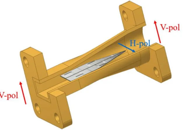
At its input and output ports, any real OMT has finite return loss (non-zero reflection) as well as a finite coupling between Ports 1 and 4 and between Ports 2 and 3, i.e. a finite cross-polarization level. In addition, the coupling between Port 3 and Port 4, the output Isolation, is finite (non-zero coupling). In modern radio-astronomy receivers, typical requirements of the OMT are a high cross-polarization discrimination between the orthogonal signals (XP>30 dB,) low insertion loss (a few tenths of a decibel), and a good match of all electrical ports (return loss above 20 dB) over bandwidths of 30% or wider. An example of the specifications of the reverse-coupler W-band OMT [8], shown in Fig. 2, is given in Table 1.
OMTs for millimeter and sub-millimeter wavelengths are typically based on waveguide structures. The OMT input common port could be either a square or a circular waveguide, while the two outputs adopt rectangular waveguides, mostly standard. While the OMT waveguide outputs are chosen to operate in single-mode (TE10) across the design band, the input waveguide necessarily allows propagation of
multiple modes: at least the two orthogonal modes TE10 and TE01, associated to Pol 1 and Pol 2,
propagate in a OMTs with square waveguide input. Similarly, at least the two orthogonal modes TE11
associated to Pol 1 and Pol 2, propagate in OMTs with circular waveguide input. Higher order modes might also propagate in the square or circular waveguide common port, at least in the higher part of the
5
Fig. 2: Photos of the reverse-coupler W-band OMT with waveguide test transitions, see reference [8] for more details. The OMT has a square waveguide input (2.54×2.54 mm2), a WR10 waveguide output and an oval
waveguide output matched to WR10. Standard UG387 flanges are used at all ports.
Parameter Associated parameter
Specification
Frequency range - 84-116 GHz
Insertion Loss of polarization signal VP from Port 1 to output Port 3, 𝐼𝐿31 |S31| <0.5 dB
Insertion Loss of polarization signal HP from Port 2 to output Port 4, 𝐼𝐿42 |S42| <0.5 dB
Input Return Loss of polarization signal VP at Port 1, 𝐼𝑅𝐿11 |S11| >20 dB
Input Return Loss of polarization signal HP at Port 2, 𝐼𝑅𝐿22 |S22| >20 dB
Output Return Loss of polarization signal VP at Port 3, 𝑂𝑅𝐿33 |S33| >20 dB
Output Return Loss of polarization signal HP at Port 4, 𝑂𝑅𝐿44 |S44| >20 dB
Cross-polarization of polarization signal VP from Port 1 to output Port 4, 𝑋𝑃41 |S41| >30 dB
Cross-polarization of polarization signal HP from Port 2 to output Port3, 𝑋𝑃32 |S32| >30 dB
Isolation between Port 3 and Port 4, ISO43 |S43| >30 dB
Isolation between Port 4 and Port 3, ISO34 |S34| >30 dB
Table 1: OMT Specification to be met at the physical temperature of 293 K. The OMT operating temperature is 20 K.
bandwidth: the TE11 and TM11 modes in the square waveguide, the TM01 mode (single polarization) and
the two polarizations of the TE21 mode in the circular waveguide. However, OMTs are generally
designed to avoid the excitation of higher order modes to avoid unwanted difficult-to-control effects and mode conversion. This is achieved mostly by adopting symmetry properties in the geometry of the OMT waveguide structure. As a consequence, broadband OMT design requires in general a high degree of symmetry of its 3D internal structure. Misalignments or tolerance errors in the mechanical construction of the OMT can lead to the excitation of the unwanted higher order modes. This is more critical for high-frequency OMTs, as the requirements on mechanical fabrication and alignment tolerances are more stringent. Typically, mechanical tolerances of less of about one percent of the wavelength are required: for example, about ±10 µm are required for OMTs operating around 3 mm band (100 GHz) and about ±5 µm for those operating around the 1.3 mm band (230 GHz).
Here, we assume that only two orthogonal modes can propagate in the common OMT square or circular waveguide input, and that the 4×4 S-parameter matrix given in Eq. (1), provides a full and accurate representation of the OMT performance. In particular, we ignore the effects of possible higher order modes that could potentially propagate in the common OMT arm. If excited, those modes should be taken into account and an S-matrix with more than four ports be defined (and properly measured). For example, if four modes propagate in the input OMT common port, a six-port S-matrix would be required to correctly represent the OMT properties (assuming the OMT outputs are single-mode).
OMT characterization methods
We assume the OMT adopts a circular waveguide input and two rectangular waveguide outputs with standard UG387 waveguide flanges. Specifically, a 2.93 mm diameter input waveguide port (Port 1 and Port 2 of Fig. 1) and two WR10 output waveguides (Port 3 and Port 4) are adopted for the W-band
6
(3 mm band) OMT, to which we will refer below. The characterization methods we will describe for this OMT can be adapted and extended to other OMT designs and for other bands.
Waveguide transitions, waveguide parts with constant waveguide cross-section, 90° waveguide bends and twists are required for these tests. Here, we remind that the physical length of such parts is associated to their electrical properties and in particular, that the guided wavelength g of a wave propagating in waveguide is frequency-dependent and related to the propagation constant through the following:
𝛽() =2 𝜋
𝑔() (13) where is the frequency and:
𝑔()=
√1−( 𝑐)
(14)
with c being the cut-off wavelength of the mode under consideration (c=2 a for the TE10 mode in
rectangular waveguide, a being the waveguide wider size and c=(π/p′) D for the TE11 mode in
circular waveguide, and D being the waveguide diameter and p′ ≈ 1.841 the first zero of the first-order first-kind Bessel function derivative J1′).
For example, at the central frequency of the 70-116 GHz band, 93 GHz, the value of the propagation constant in WR10 waveguide of the fundamental TE10 mode is (93 GHz)=1506 1/m, corresponding
to a g(93 GHz)=4.17 mm. In a circular waveguide with diameter of 2.93 mm, the propagation constant
of the fundamental TE11 mode at 93 GHz is (93 GHz)=1489 1/m, corresponding to a
g(93 GHz)=4.21 mm.
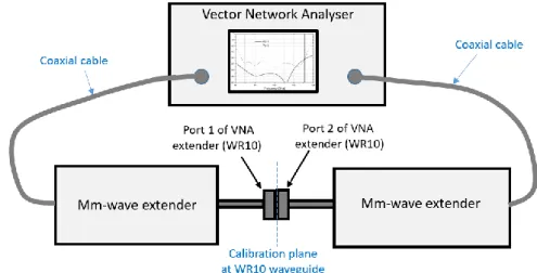
Required test equipment
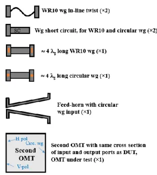
The following hardware is required to perform a full testing of the W-band OMT, i.e. the complete characterization of the S-matrix in eq (1), using the various characterization methods that will be described in the following subsections. A schematic diagram for each of them is shown in Fig. 3.
7
Fig. 3: Schematic representation of the waveguide test equipment required for full test of the OMT using the various characterization methods. It is assumed that the OMT has a circular waveguide input port, whose test requires adoption of circular waveguide parts: quarter-wave long and 4 g long circular waveguide parts,
WR10-to-circular waveguide transition, and feed-horn with circular waveguide input. In case the OMT has a square waveguide, the equivalent parts in square waveguide (rather than circular waveguide) are required. If the OMT has custom flanges, rather than standard UG387 flanges, suitable transitions between flanges with constant waveguide cross-section are needed (see bottom left). Rectangular waveguide twists and E- and H–plane bends are also required for connection to the VNA. If available, a second OMT can be used for additional tests of the OMT (bottom right).
Only a subset of the equipment listed below is required for a specific characterization method: 1. A Vector Network Analyser (VNA) with WR10 extenders operating across the full OMT
band, assumed to include the standard 75-110 GHz band. For this OMT example, the frequency band of the VNA should cover 70-116 GHz. We name it “VNA”;
2. Two WR10-to-2.93 mm circular waveguide transitions (with UG387 flange at both ends). We name them “WR10-to-circ” transition. The single transition will be approximately 3 to 4 guided wavelengths long (3-4 g) at the central frequency, and might be similar to the one
shown in Fig. 4. These two transitions will be tested back-to-back and calibrated out when necessary (see further down for details).
3. Two waveguide short circuits (with UG387 flange), i.e. a flat metal surface, with high-electrical conductivity, orthogonal to the waveguide propagation direction. The flatness and orthogonality requirement allows avoiding excitation of higher order modes and should allow perfect reflection of the incoming waves with no RF leakage and negligible electrical losses at the interface plane of the waveguide to which it is attached. We name the waveguide short “WG SC”. Note that the waveguide short circuits will be used both as a termination for the 2.93 mm diameter circular waveguide and for the WR10 rectangular waveguide;
4. One WR10 quarter-wave long rectangular waveguide section. This is usually part of the WR10 calibration kit of the VNA (for TRL or other calibration methods). The length of the quarter-wave section is approximately 1.0 mm for the TE10 mode at the central frequency of
W-band (g/4). This length must not be a given exact value, but must be known with high
8
5. One 2.93 mm diameter quarter-wave long circular waveguide section. The length of the quarter-wave section is approximately 1.0 mm for the TE11 circular waveguide mode at the
central frequency of W-band. This length must not be a given exact value, but must be known with high accuracy as it will be used in the calibration process;
6. One 2.93 mm diameter circular waveguide section with length of at least 4 guided wavelengths, i.e. at least 16 mm long. The length value does not need to be very precise. This waveguide section will be used for time domain VNA test of the OMT to more accurately separate the reflections from feed and OMT and determine the correct time-gating position that allows removal of the feed-horn reflection effect. Note that in higher frequency OMTs (such as ALMA Band 6, 211-275 GHz, or ALMA Band 8, 385-500 GHz) the 4 guided wavelengths section length may not be practical, given the flange to flange length consideration. For mechanical construction reason, the 4 guided wavelengths is a lower bound for the length of the waveguide section at sub-mm waves;
7. One well-matched load in circular waveguide. This is a conical absorber, with electrical length of approximately 3-4 g, mounted inside a circular waveguide with the same diameter
as the input waveguide of the OMT (2.93 mm in this specific case);
8. One well-matched feed-horn, with 2.93 mm output waveguide connected to the OMT input common port circular waveguide (with 2.93 mm diameter). With “well-matched” we intend a feed with input reflection possibly 10 dB lower (better) than the OMT, i.e. if the OMT has -20 dB reflection, then the well-matched feed will have -30 dB reflection (worst case). 9. One second OMT, with cross-section of input and output waveguide identical to the OMT
under test. Ideally, the second OMT is a copy of the OMT to be tested, so that the performances of the two units are ideally identical and can be more easily accounted for in the estimated performance of the single device.
Fig. 4: 3D sketch of one circular-to-rectangular transition (associated to the first symbol on top of Fig. 4). Two of these transitions, connected back-to-back, are used in one of the OMT testing methods. In this example, the rectangular waveguide is WR10 (2.54×1.27 mm2) the circular waveguide diameter is 2.93 mm and the transition
is 15 mm, about 3.6 g(93 GHz) of the rectangular waveguide TE10 mode. The input reflection is less than -30 dB
across 70-116 GHz.
Considerations on circular waveguide-to-rectangular waveguide transition
The goal of a transition between rectangular and circular waveguide (item 2 of the above list,
WR10-to-circ) is to transform the E-field of the TE10 mode injected from the WR10 waveguide of the VNA
extender into a pure TE11 mode at the 2.93 mm diameter circular waveguide output of the transition,
whose polarization is parallel to the one of the TE10 mode in WR10. In a real situation, the mechanical
fabrication and misalignment errors will cause the excitation of the unwanted orthogonal TE11 mode at
the circular waveguide transition output, i.e. the transition will have a finite cross-polarization level. In particular, due to the unavoidable fabrication imperfections, a real WR10-to-circ transition might produce at its output an orthogonal TE11 mode with a non-zero phase difference relationship with the
9
transition to be elliptically polarized, as shown on the left panel in Fig. 5. However, our experience with real transitions fabricated in W-band shows that the cross-polarization effects associated with the phase shift between the two orthogonal TE11 modes, i.e. the elliptical polarization component (minor axis of
the polarization ellipses) is typically negligible with respect to the amplitude of the orthogonal TE11
mode, i.e. to the linear polarization part: The signal at the output of the circular waveguide is linearly polarized and has an E-field polarization at a small angle to the input E-field excitation at the WR10 input, as shown on the right panel in Fig. 5. In the linear polarization case, the excitation of the cross-polarization component, in principle, can be corrected by a relative rotation between the contact flanges: full correction at a particular frequency or optimized to minimum cross-polarization contamination over the full bandwidth. In the elliptical polarization case, the full correction is not achievable and it is only possible to correct by relative flange rotation up to the minimum cross-polarization contamination associated with the level of the minor axis of the polarization ellipsis.
Fig. 5: Sketch of the electric-field orientation injected at the OMT circular waveguide input. The ideal polarization orientation of the E-field vector associated to the TE11 mode is represented by the “H-pol” vector (in blue), while
the actual orientation is depicted with “Injected pol” (in red). The left panel refers to the general case of the elliptical cross-polarization, while the right panel refers to the case of linear cross-polarization. The slight angle between the two vectors on the right panel (here exaggerated for better clarity) is due to the cross-polarization of the adapter, assumed to generate linear cross-pol (and negligible elliptical cross-pol). In addition, the minor axis of the polarization ellipsis on the left panel has been exaggerated for clarity.
The cross-polarization level of the circular-to-rectangular transitions that we have tested in W-band through their back-to-back cross connection is typically of order -30 dB, i.e. of the same level (or worse) of the OMT cross-polarization. In this respect, circular-to-waveguide transitions for mm and sub-mm wave are usually not suitable for a standalone direct test of the OMT cross-polarization level. An alternative and complementary test method of the cross-polarization is often necessary for accurate characterization. This is based on the short circuited OMT input that will be discussed further down. When the OMT is tested with the circular waveguide-to-rectangular waveguide transition at its input, the port associated to the orthogonal mode is not properly terminated into a matched load since it presents a reactive load. In particular, the OMT circular waveguide input will have an unmatched Port 2 when measuring S31 or S41, and an unmatched Port 1 when measuring S42 or S32.
The following considerations are valid in all measurements that require the use of the adapter at the OMT input, i.e. the insertion losses S31 and S42 and the cross-polarizations S41 and S32. The error is
mainly due to a combination of the OMT return loss and of the adapter cross-polarization, which corresponds to the signal fully reflected back from the port associated to the orthogonal mode (Port 2 when S31 measurement is considered). Typical OMT and adapter performance lead to an estimate of
10
this error contribution of about -50 dB, assuming the OMT has a reflection coefficient of -20 dB (magnitudes of S11 and S22) and the adapter has a cross-polarization of about -30 dB:
1) Error in insertion loss measure with adapter. Let us consider the example of S31
measurement. When measuring the S31 scattering parameter (see Fig. 1), Port 2 is not matched,
as ideally required, and the |S22| reflection is not 0. Therefore, there is an error associated to this
measurement of the OMT with the adapter, i.e. the estimated -50 dB error, as previously discussed, minus the cross-polarization (in dB), resulting in a typical value of -80 dB in total. This reflected signal combines with the S31 parameter under measurement and is clearly a
negligible error in the measurement of the insertion loss S31, which is expected to be of few
tenths of a dB.
A similar reasoning holds also for S42.
2) Error in cross-polarization measure with adapter. Let us consider the example of S41 measurement. When measuring the cross-polarization associated to the S41 scattering parameter
(see Fig. 1), Port 2 is not matched, as ideally required, and the |S22| reflection is not 0. Therefore,
the same error of -50 dB previously estimated in the insertion loss measure also holds in this case. However, this error combines differently to the output signal as it is associated to the S42
parameter, which is close to few-tenths of a dB. Thus, we expect a level of -50 dB at Port 4 due to this error, to be compared with S41 parameter that is of the order of about -30 dB, typical.
Thus, this effect is not negligible as in the previous case of the insertion loss measure. A similar reasoning holds also for S32.
To avoid the error associated with the improper termination of the orthogonal mode of the OMT in measuring the insertion loss and cross-polarization, a second OMT can be used. The second OMT can be connected with its common port to the common port of the OMT under test. Let us assume the two OMTs have identical input waveguide cross-sections and similar performance. Thus, connecting the two OMTs back-to-back, the two orthogonal modes at the input of the OMT under test (Port 1 and Port 2 of Fig. 1) are both terminated to a matched load (with return loss equal to the input return loss of the second OMT), so that both modes can be independently excited, while simultaneously providing a good match.
Calibration procedures
The TRL (Thru-Reflect-Line) calibration technique2 is adopted. The TRL calibration relies only on the
characteristic impedance of a short transmission line. From two sets of two-port measurements that differ by this short length of transmission line and two reflection measurements, the full 10-term error model can be determined. Many different names have been given to this overall approach - Self Calibration, Thru-Short-Delay, Thru-Reflect-Line, Thru-Reflect-Match, Reflect-Line, Line-Reflect-Match, and others. These techniques are all variations of the same basic approach. Advanced forms are TRM, LRM, LRL and LRRL.
The TRL has some advantages over the other commonly used calibration technique, the SOLT, which is based on Short, Open, Load, and known-Thru standards with 12-term error model:
- The use of standards that are easy to fabricate and have simpler definitions than SOLT; - The need of only transmission lines and high-reflect standards;
- Minimum requirement of impedance and approximate electrical length of line standards; - Reflect standards can be any high-reflection standards like shorts or opens;
- Load not required; capacitance and inductance terms not required;
- Potential for more accurate calibration (depends on quality of transmission line).
2 See for example the Keysight application note
11
The TRL refers to the three basic steps in the calibration process (see also Fig. 6):
THRU - connection of port 1 and port 2 of the VNA ports extender, directly or with a short length of transmission line;
REFLECT - connect identical one-port high reflection coefficient devices to each port. This is achieved by connecting the waveguide short circuit “WG SC” to both VNA ports;
LINE - insert a short length of transmission line between port 1 and 2 (different line lengths are required for the THRU and LINE). This is achieved by connecting the quarter-wave waveguide between the reference plane of the calibration: a) a quarter-wave WR10 waveguide section between the two WR10 ports of the VNA extender, when the calibration plane reference is at the WR10 VNA ports; b) a quarter-wave 2.93 mm diameter waveguide section between the 2.93 mm diameter waveguide sections of the WR10-to-circular transition “WR10-to-circ”, when the calibration plane reference is at the circular waveguide port.
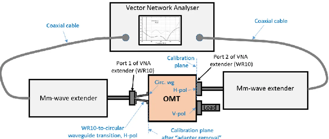
Adapter removal
As it will be clarified in the next section, one of the OMT measurement methods requires the insertion of a circular-to-rectangular waveguide transition at the OMT input. The effect of this transition can be calibrated out using the adapter removal method. Adapter Removal is a technique used to remove any adapter characteristics from the calibration plane. For example, the Keysight E5071C VNA (and similar commercial VNAs from other companies like Rohde&Schwartz or Anritzu) uses the following adapter removal process to remove adapter characteristics:
- Perform calibration with the adapter in use;
- Remove the adapter from the port and measure Open, Short, and Load values to determine the adapter’s characteristics;
- Remove the obtained adapter characteristics from the error coefficients in a de-embedding fashion.
Two TRL calibrations shall be performed:
a) Without adapter: one standard calibration at the WR10 waveguides of the VNA extender, without waveguide transition (without adapter), as shown in Fig. 6;
Fig. 6. Setup for calibration at the WR10 waveguide extenders, THRU measurement. The REFLECT measurement requires the insertion of waveguide short circuits at the two WR10 VNA extender ports. The LINE measurement require the insertion of a quarter-wave waveguide between the two WR10 VNA extender ports.
b) With adapter: one calibration with two 2.93 mm diameter circular-to-WR10 waveguide transitions connected back-to-back (Thru), as shown in Fig. 7. In this case, the calibration is
12
made in 2.93 mm diameter circular waveguide, at the interface plane between the two transitions. This TRL calibration requires the insertion of the quarter-wave circular cross-section line between the two back-to-back transitions (Line) and the insertion of the two short circuits in circular waveguide (Reflect). The adapters do not need to be identical. Their effects are saved and stored in the VNA during calibration. The effects of one of the two adapters can be removed from the OMT measurements.
Fig. 7. Setup for calibration at the circular waveguide: two WR10-to-circular waveguide transitions (adapters) are connected back-to-back with the WR10 waveguides of the mm-wave extenders parallel to each other, i.e. oriented to excite the two parallel polarization channels.
We note that when the adapter is in place, i.e. when the 2.93 mm diameter circular waveguide-to-WR10 waveguide is attached to the 2.93 mm diameter waveguide OMT input port, the orthogonal polarization of the TE11 mode in circular waveguide is not terminated into a matched load, as it would be required
for S-parameter characterization. This polarization propagates into a cavity that presents a frequency-dependent total reflection as it is in cut-off and cannot propagate through the WR10 waveguide. The orthogonal polarization is excited by very small mechanical asymmetries inside the adapters that are very hard to control and produces spikes in the bandwidth at regular stepped frequencies where calibration will thus fail. This effect can be mitigated by using thin sheet of lossy material inside the adapter, placed orthogonally to the work polarization, dumping down the resonances of the orthogonal polarization up to acceptable levels for a very good calibration. An example of this adapter with thin sheet of lossy metal parallel to the H-pol is shown in Fig. 8. The sheet also produces loss in the work polarization signal, V-pol, but it has no effect since it is taken into account in the calibration.
Fig. 8. Example of circular waveguide to rectangular waveguide transition with thin sheet of lossy material placed orthogonally to the E-field of the TE10 mode propagating in rectangular waveguide (V-pol). The orthogonal
13
OMT port access and additional waveguide parts
The waveguide components required to test the OMT depend on its design, in particular on the positioning of the two output waveguide ports with respect to the input waveguide port. In fact, different configurations for the positioning of the OMT output ports exist. A non-exhaustive list of examples is given below:
a) The two waveguide outputs are in line with the input waveguide, and have their E-planes parallel to each other (the E-field vectors of the fundamental TE10 modes in rectangular
waveguide are parallel), i.e. the two outputs are on the same face of the OMT block, opposite to the OMT waveguide input. This is usually required when the OMT is part of an array, to benefit integration of the receiver components. An example of this configuration is given in [17];
b) Same as previous, but with the H-planes of the output waveguides that are parallel;
c) The two waveguide outputs are in line with the input waveguide, and have their E-planes orthogonal to each other on the same OMT block face (similar to the two previous cases, but with output waveguide orientations at 90° to each other);
d) The two waveguide outputs are orthogonal (not in line) to the waveguide input: the two outputs are located on opposite sides of the OMT block faces, and the input is orthogonal to both of them (T-shape configuration). The orientation of the E-planes of the output waveguides (on opposite OMT block faces) are parallel;
e) Same as previous point, but with orthogonal orientation of the E-planes of the output waveguides (on opposite OMT block faces);
f) The two waveguide outputs are orthogonal (not in line) to the waveguide input, and they are also orthogonal to each other, i.e. the three access ports are located on three different and orthogonal faces of the OMT block. An example of this OMT configuration is given in [4]. g) One of the two OMT waveguide outputs is in-line with the input, while the second output is
orthogonal to the input (see for example Fig. 2 and [8]).
Depending on the OMT design, to access the input and output ports of the OMT and connect them to the VNA ports of the extenders, the adoption of different waveguide parts, like 90° twists, bends and straight waveguides is required. When possible, the VNA extension heads might be rotated by 90° around the axis of the WR10 waveguide to avoid using waveguide twists. The coaxial cables that connect the VNA to the extenders allow some degree of freedom in moving and positioning the extenders. All waveguide parts required to access the OMT ports have to be calibrated out. Care must be taken to verify that the calibration is not affected by movement of the cables and extenders. In the following, we assume that the OMT configuration is as in a) of the above list, i.e. the two output waveguides are on the same OMT block face, opposite to the input waveguide access port face, and their E-fields are parallel. No twists are required in this case. In addition, we assume that standard UG387 flanges, rather than custom flanges, are used. The waveguide bends (E-plane and H-plane) and waveguide twists will not be represented in the schematics of the measurement setups that will be discussed in the following Figs. 11-18.
Time-domain method and time gating
Time domain gating is a powerful feature in a VNA that mathematically removes the unwanted responses in time domain, by identifying the mismatches along the line under test. The function performs time domain transformation using a Fourier Transform, allows operating on the signal in the time domain and applies reverse transformation back to the frequency domain. This function is used to remove the mismatch effects of the adapters from the frequency response, if the useful signal and the mismatch signal are separable in time domain. The function involves two types of time domain gating, as shown in Fig. 9:
14
a) Bandpass – removes the response outside the gate span; b) Notch – removes the response inside the gate.
To optimize the performance with time domain gating requires to adopt windowing in frequency domain. The rectangular window shape in frequency domain leads to spurious sidelobes, due to sharp signal changes at the limits of the measurement bandwidth. Various window shapes are offered on VNAs to reduce the sidelobes (for example on Keysight VNAs shape options are maximum, wide, normal and minimum). The “minimum” window has the shape close to rectangular. The “maximum” window has a more smoothed shape. From minimum to maximum window shape, the sidelobe level increases and the gate resolution decreases. The choice of the window shape is always a trade-off between the gate resolution and the level of spurious sidelobes. Time gating and frequency windowing procedures require a lot of care in their application since they alter the levels and the spectral content of the signal. Scaling and renormalization are also required procedures and most often they are automated on the software running on the VNAs and transparent to the operator.
An example of application of gating in time domain, adapted from a Keysight application note [28], is given in Fig. 10. Here, the effects of the “Environment”, including the reflection from the metal plate, are removed by time gate bandpass to keep the reflection of the adapter and the horn.
Fig. 9. Sketch of filter responses in time domain based on “Bandpass” filter (left) or “Notch” filter (right). The original time domain responses are on top, the filtered outputs are given at the bottom.
15
Fig. 10. Time domain VNA technique to filter out undesired responses from the measurement. Top: schematic of test setup with VNA extender connected to a horn antenna through adapter and long circular waveguide. A metal plate reflects back part of the energy. Bottom: screenshot of VNA output showing the time-domain response and the time gate bandpass filter set to remove the effects of the environment.
Methods for measurements of the OMT Insertion Loss
The insertion losses of the OMT, defined by eqs. (3) and (4), can be measured using the three different methods a), b), and c) listed below:
a) With a 2.93 mm diameter circular waveguide-to-WR10 waveguide transition connected between the OMT circular input and Port 1 of the WR10 waveguide of the VNA extender, as shown in Fig. 11. Port 2 of the VNA extender is connected to the coupled polarization WR10 output of the OMT, while the uncoupled OMT WR10 output is terminated into a matched load. The effects of the circular transition are removed using the adapter removal calibration method described previously. We note that this setup can also be used for measurement of the input return loss, as explained further down.
Fig. 11. Setup for measurement of the OMT Insertion Loss with a WR10-to-circular waveguide transition (adapter). The block diagram refers to the measurement of the IL of H-polarization, associated to S31.
16
b) With a short circuit (SC) at the circular waveguide input of the OMT, as illustrated on the left panel in Fig. 12. This requires two measurements: one with the SC directly connected to the input common port of the OMT, another with the SC and OMT connected through a quarter-wave circular quarter-waveguide. The VNA extender ports are connected to the OMT quarter-waveguide outputs. Both measurements provide a total reflection of the signals from the short-circuited OMT. If we use the symbol 𝑆̅̅̅̅ (“overline S𝑖𝑗 ij”) to indicate the reflection coefficients measured
by the VNA in the setup in Fig. 12 (see right panel) and the symbol Sij to indicate the scattering
parameters of the OMT, as defined in (2), by neglecting the cross-polarization terms of both the OMT and the SC and the loss of the SC, we have:
{𝑆̅̅̅̅ ≅ 𝑆11 33− 𝑆31𝑆13⁄(1 + 𝑆11) 𝑆22
̅̅̅̅ ≅ 𝑆44− 𝑆42𝑆24⁄(1 + 𝑆22)
(15)
The derivation of eq. (15) is discussed in Appendix A. If the amplitudes of the transmissions (|S13| = | S31|, |S14| = | S41|) are assumed predominant with respect to the amplitude of the
reflections (|S11|, | S22|, |S33| and |S44|), we have that the VNA measured reflection coefficients
are the square of the OMT transmission parameters: {|𝑆̅̅̅̅| ≅ |𝑆11 31|
2
|𝑆̅̅̅̅| ≅ |𝑆22 42|2
(16)
When expressed in dB scale in terms of losses, we have: {𝐼𝑅𝐿̅̅̅̅̅̅̅ = −20 𝑙𝑜𝑔11 10|𝑆̅̅̅̅| ≅ −20 𝑙𝑜𝑔11 10 |𝑆31| 2= 2 (−20 𝑙𝑜𝑔 10|𝑆31|) = 2 𝐼𝐿31 𝐼𝑅𝐿22 ̅̅̅̅̅̅̅̅ = −20 𝑙𝑜𝑔10|𝑆̅̅̅̅| ≅ −20 𝑙𝑜𝑔22 10 |𝑆42|2= 2 (− 20 𝑙𝑜𝑔10|𝑆42|) = 2 𝐼𝐿42
(17)
that is the measured input return loss of each polarization is two times the insertion loss of the associated polarization channel (when expressed in dB scale).
It is expected that the |𝑆̅̅̅̅| and the |𝑆11 ̅̅̅̅| levels are both of order of few tenths of a dB (negative 22
values), i.e. close to 1 if expressed in linear value. However, the measurement will be affected by the presence of several spikes across the band, associated to the excitation of higher order modes that are trapped inside the OMT, whose magnitude might be greater than a few tenths of a dB. These spikes are not due to a real increase of the OMT insertion loss and are removed by the second measurement with quarter wave offset short circuit, which causes a shift in frequency of all non-real spikes. In conclusion, the insertion loss of both OMT polarization channels are simultaneously obtained after removal of the spikes from the two setups (with short circuit and offset short circuit at the OMT input).
We note that the setup of Fig. 12 allows also estimating the OMT cross-polarization, as it will be explained in section “Methods for measurements of the OMT Cross-polarization”.
17
Fig. 12. Left: Setup for measurement of the OMT Insertion Losses with a short circuit (SC) at the circular waveguide input. The measured reflection coefficient at each of the ports, divided by 2, provides an estimate of the respective ILs (associated to S31 and S42). This same setup can also be used for
characterizing the OMT cross-polarization (associated to S32 and S41). Right: S-parameter
representation and definition of scattering parameters of OMT (S-matrix with parameter Sij, neglecting
the cross-polarization terms) and of S-parameters measured from the mm-wave extender (S-matrix with parameter 𝑆̅̅̅̅). 𝑖𝑗
c) With a second OMT connected to the circular waveguide input of the OMT under test, i.e. two OMTs back-to-back, as illustrated in Fig. 13. If the OMT under test and the second OMT have identical dimensions of the input and output ports and have similar performance, their insertion loss can be obtained dividing by two the insertion loss of the two combined OMTs. If the performance of the two OMT are different, the insertion loss of the OMT under test can be obtained by subtracting the insertion loss of the second OMT, measured with one of the two previously indicated methods3. The advantage of this method over the one described at point a)
(Fig. 11) is that the second polarization channel at the input of the OMT under test (Pol H, if referring to the example of Pol V measurement of Fig. 13) is correctly terminated. However, we have seen that the error made in measuring the insertion loss with adapter in negligible.
3 In case three OMTs are available (OMT1, OMT2 and OMT3), it is possible to pair them in three possible
combinations (OMT1 with OMT2, OMT1 with OMT3, and OMT2 with OMT3). The measurement of each pair provides the total insertion losses of the pair (insertion loss of two OMTs combined), which results from the combination of the insertion losses of the individual OMTs. By measuring the total insertion losses of the three OMT pairs it is possible to derive the insertion losses of the three individual OMTs (system of three equations with three unknowns).
18
Fig. 13. Setup for measurement of the OMT Insertion Loss using a second OMT. The setup refers to the measure of Pol V insertion loss (associated to S42).
Methods for measurements of the OMT Input Return Loss
The OMT input return loss, defined by eqs. (5) and (6), can be measured using the two different methods listed below:
a) With a 2.93 mm diameter circular waveguide-to-WR10 waveguide transition connected between the OMT circular input and Port 1 of the WR10 waveguide of the VNA extender. The setup is the same one used for the insertion loss, shown in Fig. 11. The coupled polarization output of the OMT can be connected with the Port 2 of the VNA or with a matched load. The uncoupled OMT output is terminated into a matched load. The effects of the circular transition are removed using the adapter removal calibration method described previously. The measurement is repeated to characterize the return loss of both channels, after rotation of 90° around its axis of the circular waveguide-to-WR10 waveguide transition (together with the VNA extender block) at the OMT input or, better, by 90° rotating the OMT around its axis and leaving untouched the VNA port 1 extender and the transition, with major benefits in keeping the calibration accuracy (and after swapping, accordingly, the load and the VNA Port 2 at the output ports).
b) Using the VNA time-domain method. In the setup, the OMT circular waveguide input is connected to the VNA extender WR10 port 1 through a 2.93 mm diameter circular waveguide-to-WR10 waveguide transition. This is cascaded with a 4 g circular waveguide, see Fig. 14.
The circular waveguide section allows the reflection from the transition to be more accurately separated from the one of the OMT and the time gating bandpass filter more precisely be applied. In this case, the adapter removal has not to be applied since the adapter effect is filtered out by the time gating technique. The loss of both the adapter and the circular waveguide section has most often negligible influence (few tenths of a dB) on the return loss but, if high accuracy is required, it has to be characterized and taken into account in the measurement (the effect of the loss is to improve the return loss by twice the loss of the adapter plus the waveguide section). VNA extender WR10 port 2 is connected to the coupled polarization output port while the uncloupled port is terminated (as before, the VNA port 2 can be replaced with a matched load).
19
Fig. 14. Setup for measurement of the OMT Input Return Loss (associated to S11 and S22) with a 4g
long circular waveguide connected at the OMT input. Time-gating is used in time-domain to remove the reflections from the WR10-to-circular waveguide transition connected to the OMT input. The 4g long
circular waveguide section allows a more precise determination of the reflection peaks due to the test transition. The setup refers to the measure of both IRLs. Port 2 of the mm-wave VNA extender can be replaced by a waveguide matched load.
Methods for measurements of the OMT Output Return Loss
The OMT output return loss, defined by eqs. (7) and (8), can be measured using the three different methods a), b), and c) listed below. While method a) and b) provide a good estimate of the OMT ORL in most cases, method c) can be used when a more accurate measurement is required, for OMT with very good expected return loss of the order or greater than 30 dB:
a) With a circular waveguide matched load attached to the 2.93 mm diameter circular waveguide of the OMT, and with OMT Port 3 and Port 4 connected to the WR10 ports of the VNA extender (respectively Port 2 and Port 1). The setup is shown on the left of Fig. 15. The matched load is commonly fabricated using a conical shaped lossy material inside a circular waveguide. The measurement accuracy relies on the quality of the conical load, which is expected to be better than -30 dB across the full band.
20
Fig. 15. Left: Setup for measurement of the OMT Output Return Loss (associated to S33 and S44) with a
circular waveguide load connected at the OMT input. The conical load provides a good match for both polarization channel and the return losses are measured for both outputs with a single setup. Right: a similar setup adopting a well-matched feed-horn in place of the circular waveguide load. The feed-horn must be terminated into an external absorber (not represented). These two setups can also be used to measure the OMT isolation.
b) With a well-matched feed-horn attached to the 2.93 mm diameter circular waveguide of the OMT, and with Port 3 and Port 4 connected to the WR10 ports of the VNA. The setup is shown on the right of Fig. 15. The measurement relies on the quality of the feed-horn, which is expected to be better than 30 dB return loss across the full band.
An alternative to this configuration, which adopts the feed-horn, is to leave the OMT circular waveguide open, radiating to free space (or also faced to external absorbers). In fact, the two orthogonal TE11 circular waveguide modes in circular waveguide are well-matched across the
upper part of the operating band. For example, the maximum reflection over 70-116 GHz of an open 2.93 mm waveguide is in the range -22 to -37 dB (the highest reflection, -22 dB, is at the lowest frequency of 70 GHz. The reflection is below -30 dB above 80 GHz). This is as good as most feed-horns. However, the matching of the circular open ended waveguide strongly depends on the circular diameter and on frequency, so that this should be evaluated case by case. An open square waveguide could also quite-well matched as the circular one. For example, a 2.54×2.54 mm2 square waveguide has a reflection in the range -30 to -20 dB across
70-116 GHz (the highest reflection, -20 dB, is at the lowest frequency of 70 GHz. The reflection is below -25 dB above 75 GHz). For a comparison, the maximum reflection over 70-116 GHz of an open WR10 waveguide is in the range -10.5 to -14 dB.
c) If the return loss of the circular waveguide conical load or of the feed-horn (or opened circular waveguide) used in the previously described setups of Fig. 15 is of the same order as the OMT expected ORL, and a more accurate characterization of the OMT ORL is required, then a time domain method can be used. The test setup, making use of an added 4 g long circular
21
waveguide section connected to the OMT input, is shown in Fig. 16. The circular waveguide section is opened on external absorbers, reproducing a matched load. The effects of the open-ended circular waveguide can be removed with time gating and the ORL of the OMT be measured simultaneously for both output waveguides of the OMT.
Fig. 16. Setup for measurement of the output return losses of the OMT (associated with S33 and S44) using the
time domain method. The effects of the reflection at the opening of the circular waveguide are more easily separated from the contribution of the OMT internal structure using a 4 g long circular waveguide section
connected to the OMT input. The effects of the opened circular waveguide are thus better removed by time gating. This setup can also be used to measure the OMT isolation.
Methods for measurements of the OMT Cross-polarization
The OMT cross-polarization, defined by eqs. (9) and (10), can be measured using the three different methods a), b), and c) listed below:
a) With a 2.93 mm diameter circular waveguide-to-WR10 waveguide transition connected between the OMT circular input and Port 1 of the WR10 waveguide of the VNA extender, as shown in Fig. 17. Port 2 of the VNA extender is connected to the uncoupled polarization WR10 output of the OMT, while the coupled OMT WR10 polarization output is terminated into a matched load. The return loss and insertion loss effects of the circular transition are removed using the adapter removal calibration method described previously, although their effect can be neglected in this case. The setup is similar to the one described in Fig. 11 for measuring the OMT insertion loss, but with mm-wave extender Port 2 and load swapped at the OMT output ports. The main limitation of this method is the finite cross-polarization of the adapter itself, which is often of the same order of magnitude than the one of the OMT, as previously described.
22
If the elliptical cross-polarization effects of the rectangular-to-circular waveguide transition are negligible, while its linearly polarized cross-polarization effect are not, the polarization injected by the adapter into the OMT circular waveguide is linear but not orthogonal (i.e. not exactly 90° rotated) to the coupled polarization channel, as shown on the right panel in Fig. 5, where we assume the H-polarization is the coupled one. If a centring ring is used as the primary alignment mechanism (type IEEE 1785-2b, see ref. [29]) at the OMT circular input, or if the alignment dowel pins can be removed from the input UG387 flange, then it should be possible to rotate the OMT with respect to the adapter in order to determine a minimum of transmission between the VNA ports. The minimum is obtained when the injected polarization is aligned with the H-pol, i.e. when the electric fields are parallel. In that configuration, the measured transmission is the cross-polarization of the OMT, as the cross-polarization effects of the adapter have been removed.
Fig. 17. Top: Setup for measurement of the OMT cross-polarization with a WR10-to-circular waveguide adapter. In the represented setup, the adapter is rotated to excite the H-polarization of the OMT circular waveguide and refers to the measure of S41. The transmission from the OMT input to the uncoupled
V-polarization output provides the cross-V-polarization of the OMT in case the adapter is ideal, i.e. it does not contribute to the cross-polarization and reflection.
b) With a short circuit (SC) at the OMT circular waveguide input, as illustrated in the setup of Fig. 12 (left panel). The cross-polarization of the OMT can be estimated by measuring the transmission between the two OMT rectangular waveguide outputs when the device input is terminated into a short circuit. The signal injected from one of the OMT output waveguides, for example H-pol at Port 4 of OMT of Fig. 12 (VNA Port 1), travels through the internal OMT waveguide circuitry; only a small fraction of that signal is directly coupled to the other OMT waveguide output (Port 3 of OMT, V-pol) through the internal OMT structure. This fraction of the directly coupled signal is the OMT isolation, which is typically very small, of the same order of the cross-polarization value or lower. Therefore, the wave from the H-pol of the OMT rectangular waveguide output is almost fully directed towards the short-circuited OMT input, where it is reflected back with the same polarization state by the short circuit. This is equivalent at injecting the polarization signal directly from the circular waveguide input port (except for the small difference due to the device insertion loss). Therefore, the signal level measured at the other OMT rectangular port (OMT Port 3, V-pol, i.e. Port 2 of VNA extender) provides an estimate of the OMT cross-polarization, because it is equivalent at measuring the signal coupling between Pol-H channel at the OMT common port and at its rectangular waveguide output V-Pol (OMT Port 3). If the quality of the short circuit connected to the OMT circular
23
waveguide input is high (negligible electrical losses and negligible generation of spurious modes), and if the OMT isolation is much greater (much better) than the cross-polarization, this method provides an accurate measure of the OMT cross-polarization value.
c) With a second OMT connected to the circular waveguide input of the OMT under test, as illustrated in Fig. 18. If the OMTs are identical and have identical polarization, the cross-pol level of the single unit is up to 6 dB lower than the measured value of the combined OMTs (6 dB being the worst case, when the waves combine in-phase and the cross-polarization level is much lower than the insertion loss). If the pol of the two OMTs are different, the cross-pol of the unit under test can be derived after subtraction of the cross-cross-polarization of the second OMT, tested using one of the two previously described methods.
Fig. 18. Setup for measurement of the OMT cross-polarization using a second OMT. The setup refers to the measure of Pol V cross-polarization (associated to S42).
Methods for measurements of the OMT Isolation
The OMT isolation, defined by eqs. (11) and (12), can be measured using the same setups presented in Figs. 15 and 16 for the output return loss, using the three methods described in that section “Methods for measurements of the OMT Output Return Loss”. The isolation is associated to the coupling between the two OMT waveguide outputs (transmission between them) when the OMT circular waveguide input is terminated with a matched load. An accurate measure of the isolation can be obtained with the methods described in a) and b) of that section, by using the S21, S12 readouts of the VNAs (S11 and S22
give the OMT ORL). For most OMTs, an accurate isolation measure is simply obtained by letting the OMT circular waveguide radiate towards external absorbers. The contribution of the reflection from opened circular waveguide to the isolation, the measured transmission in this case, is negligible, of less than 30 dB lower than the OMT cross-polarization.
24
Appendix A
Derivation of equation (15)
In Fig. A1, an OMT, characterized by the scattering matrix
𝑆 = [ 𝑆11 𝑆12 𝑆13 𝑆14 𝑆21 𝑆22 𝑆23 𝑆24 𝑆31 𝑆32 𝑆33 𝑆34 𝑆41 𝑆42 𝑆43 𝑆44 ]
(A1)
is loaded at its common port by a reflective device, that we assume to present two different complex value reflectance’s, ρ1 and ρ2, loading the two electrical input ports, port 1 and port 2.
Fig. A1. Schematic representation of an OMT and definition of incident and reflected waves, with common port (port 1, and port 2) loaded with two different loads characterized by complex reflectance’s (ρ1 and ρ2).
If we indicate with ai and bi, i = 1,...4, the wave amplitudes, respectively, incident and reflected at the
OMT electrical ports, we have for ports 1 and 2: {𝑎𝑎1 = 𝜌1𝑏1
2= 𝜌2𝑏2
(A2)
We can use a matrix notation for (A2) as:
𝒂 = 𝜌𝒃
(A3) Where: 𝒂 = [𝑎𝑎1 2],
𝒃 = [ 𝑏1 𝑏2]
(A4)
are the amplitudes of the wave vectors at electrical ports 1, 2 and where: 𝜌 = [𝜌01 𝜌0
2]
(A5)
is the reflectance matrix at electrical ports 1, 2.
By definition of the scattering matrices, when port 4 is matched (a4= 0), we can write the reflected wave
amplitude bi, i = 1, 2, 3, as:
{𝑏3= 𝑆33𝑎3+ 𝒔3𝑎
𝑇 𝒂
𝒃 = 𝑠𝒂 + 𝒔𝑏3𝑎3
(A6)
where the two new vectors:
𝒔3𝑎= [𝑆𝑆31
32],
𝒔𝑏3= [
𝑆13
𝑆23]
(A7)
and the new matrix:
S
3
4
1
2
a
4a
3b
4b
3a
2a
1b
2b
1ρ
1ρ
225 𝑠 = [𝑆𝑆11 𝑆12
21 𝑆22]
(A8)
are defined as a function of the OMT scattering parameters. In eq. A6, the superscript “T” indicates the transpose of the matrix, i.e. the operator that switches the row and column indices of the matrix by transforming a column vector in a row vector (and vice-versa). Substituting (A3) in the second equation of (A6) we have:
(𝜌−1− 𝑠) 𝒂 = 𝒔𝑏3𝑎3
(A9)
where 𝜌−1 indicates the inverse of the reflectance matrix 𝜌. Solving for a in (A9) and substituting in
the first of (A6):
𝑏3= 𝑆33𝑎3+ 𝒔3𝑎𝑇 (𝜌−1− 𝑠) −1
𝒔𝑏3𝑎3
(A10)
Dividing all members in (A10) by a3, we have at the left side of (A10) the 𝑆̅33 reflection coefficient
term of the OMT with electrical ports 1 and 2 loaded, as in Fig. A1, by reflectance ρ1 and ρ2:
𝑆̅̅̅̅ = 𝑆33 33+ 𝒔3𝑎𝑇 (𝜌−1− 𝑠) −1 𝒔𝑏3 = 𝑆33+ [𝑆31 𝑆32] [ 1 𝜌1− 𝑆11 𝑆12 𝑆21 1 𝜌2− 𝑆22 ] −1 [𝑆𝑆13 23]
(A11)
Analogously, when port 3 is terminated (a3= 0) we can write the reflected wave amplitude bi, i = 1, 2, 4,
as:
{𝑏4= 𝑆4𝑎4+ 𝒔4𝑎
𝑇 𝒂
𝒃 = 𝑠𝒂 + 𝒔𝑏4𝑎4
(A12)
where two new vectors:
𝒔4𝑎= [
𝑆41
𝑆42],
𝒔𝑏4= [
𝑆14
𝑆24]
(A13)
and the same matrix as defined in (A8) are used. Substituting (A3) in the second of (A12) we have:
(𝜌−1− 𝑠) 𝒂 = 𝒔𝑏4𝑎4
(A14)
and solving for a in (A14) and substituting in the first of (A12) we have: 𝑏4= 𝑆44𝑎4+ 𝒔4𝑎𝑇 (𝜌−1− 𝑠)
−1
𝒔𝑏4𝑎4
(A15)
Dividing all members in (A15) by a4, we have at the left side of (A15) the 𝑆̅44 reflection coefficient
term of the OMT with electrical ports 1 and 2 loaded, as in Fig. A1, by reflectance ρ1 and ρ2:
𝑆̅̅̅̅ = 𝑆44 44+ 𝒔4𝑎𝑇 (𝜌−1− 𝑠) −1 𝒔𝑏4 = 𝑆44+ [𝑆41 𝑆42] [ 1 𝜌1− 𝑆11 𝑆12 𝑆21 1 𝜌2− 𝑆22 ] −1 [𝑆𝑆14 24]
(A16)
Equations (A11) and (A16) are a more general form of (15). If we neglect the cross-polarization terms of both the OMT (𝑆32= 𝑆23 = 𝑆41= 𝑆14= 𝑆21= 𝑆12= 0) and the SC (the off-diagonal terms in (A5)
are assumed zero) and the loss of the SC (𝜌1= 𝜌2= −1) we have that (A11) and (A16) become

![Fig. 2: Photos of the reverse-coupler W-band OMT with waveguide test transitions, see reference [8] for more details](https://thumb-eu.123doks.com/thumbv2/123dokorg/8095630.124759/6.892.111.781.111.308/fig-photos-reverse-coupler-waveguide-transitions-reference-details.webp)