Autore:
Filippo Costa ______________
Relatori: Presidente del Corso: Prof. Agostino Monorchio ______________ Prof. Marco Raugi _____________ Prof. Giuliano Manara ______________ Prof. Paolo Nepa ______________Analysis and Modeling of High-Impedance
Surfaces for the Design of Electromagnetic
Absorbers and Antennas
Anno 2010
UNIVERSITÀ DI PISA
Scuola di Dottorato in Ingegneria “Leonardo da Vinci”
Corso di Dottorato di Ricerca in
Applied Electromagnetism in electrical and biomedical
engineering, electronics, smart sensors, nano‐technologies
SSD ING‐INF/02Analysis and Modeling of High‐Impedance Surfaces for the Design of Electromagnetic Absorbers and Antennas Dipartimento di Ingegneria dell’Informazione Università di Pisa Copyright © Filippo Costa, 2010 Manuscript Accepted on January 19, 2010
If a man will begin with certainties,
he shall end in doubts,
but if he will content to begin with doubts,
he shall end in certainties.
Francis Bacon (1562 – 1626)
Truth is ever to be found in simplicity,
and not in the multiplicity
and confusion of things
Isaac Newton (1643 – 1727)
Abstract
High‐impedance surfaces (HIS) are resonant cavities synthesized by printing a periodic frequency selective surface (FSS) on the top of a grounded dielectric slab. The use of such metasurfaces allows to achieve remarkable improvements in the performance of several microwave devices.
The first part of the thesis is dedicated to the modeling of high‐impedance surfaces and frequency selective surfaces which constitute the key element of the HIS structures. A model for analyzing frequency selective surfaces is first introduced and then employed also in the analysis of high‐impedance surfaces. The circuital approach is also employed to derive a new definition of the bandwidth of the metasurfaces.
High‐impedance surfaces are employed in the design of low‐profile antennas and ultra‐thin electromagnetic absorbers. In the latter case thin high‐impedance surfaces are used to replace the typical quarter‐wavelength grounded dielectric slab making the absorbing structure much thinner. Most part of this thesis is dedicated to this issue and in particular the physical mechanisms leading to the absorption of electromagnetic waves are studied by the aforementioned transmission line model. Different designs based on resistive frequency selective surfaces for synthesize thin, wideband and lightweight absorbers with enhanced performances with respect to the available solution are proposed and analyzed. Other techniques as the use of vias as instrument to enlarge the operating bandwidth for oblique incidence and the use of the HIS boundary in place of the electrical one in classical commercial absorbers are proposed.
High‐impedance surfaces are also employed as ground plane for make an horizontal dipole to radiate efficiently. In this configuration, the interaction between the wire antenna and the high‐impedance surface excites complex waves and generates different resonant phenomena that require a rigorous analysis. The problem is thoroughly analyzed by breaking up the problem in two different contributions depending on the surface waves that are allowed to propagate in the HIS structure and important design rules are derived. The validity of the homogeneization models for approximating the finite antenna structure is also addressed. The last part of the thesis deals with the so‐called Fabry‐Perot antenna in
which high‐impedance surfaces are used to strongly reduce the height of this antenna which typically is equal to a half wavelength. In particular the thesis describes an active structure which is able to work as a tunable high‐gain antenna over a wide band.
The presented theoretical work is supported by several experimental demonstrations.
Sommario
Le Superfici ad alta Impedenza (HIS) sono cavità risonanti sintetizzate stampando una superficie selettiva in frequenza periodica su un substrato dielettrico con back metallico. L’uso di queste nuove superfici (metasuperfici) permette di conseguire importanti miglioramenti nelle prestazioni di numerosi dispositivi a microonde.
La prima parte della tesi è dedicata alla modellizzazione di superfici ad alta impedenza e superfici selettive in frequenza le quali costituiscono l’elemento chiave delle HIS. Un modello per le superfici selettive in frequenza è inizialmente introdotto e poi in seguito impiegato anche nell’analisi di superfici ad alta impedenza. L’approccio circuitale è inoltre impiegato per derivare una nuova definizione della banda delle cosiddette metasuperfici.
Le superfici ad alta impedenza sono impiegate sia per progettare antenne sia assorbitori elettromagnetici ultra‐sottili. Nel caso degli assorbitori, la superfici ad alta impedenza sono impiegate al fine di sostituire il tipico strato di dielettrico con back metallico pari ad un quarto di lunghezza d’onda in modo tale da realizzare una struttura molto più sottile. Parte della tesi è dedicata all’argomento degli assorbitori ed in particolare sono studiati, attraverso il sovra menzionato modello a linea di trasmissione, i meccanismi fisici alla base dell’assorbimento delle onde elettromagnetiche. Diversi design di assorbitori resistivi sono analizzati con la finalità di sintetizzare sia strutture a banda stretta sia strutture a banda larga con prestazioni molto migliorate rispetto alle soluzioni esistenti. Sono state inoltre analizzate tecniche progettuali che vedono l’impiego di vias metalliche per migliorare l’assorbimento ad incidenza obliqua per la polarizzazione TM e l’impiego di superfici ad alta impedenza da usare in luogo del back metallico in assorbitori di Salisbury convenzionali.
Le superfici ad alta impedenza sono inoltre impiegate nella realizzazione di antenne come piano di massa in modo tale da permettere ad un dipolo posto orizzontalmente alla superficie di irradiare efficientemente. In questa configurazione, l’interazione tra l’antenna e la superficie HIS da luogo ad onde complesse le quali generano differenti fenomeni risonanti. Tale problema è analizzato rigorosamente
scomponendolo in due diversi contributi a seconda delle onde superficiali che sono supportate dalla struttura. Tale analisi ha permesso di ricavare interessanti regole di progettazione della struttura. Inoltre è analizzata la validità dei modelli basati sull’omogeneizzazione per approssimare la struttura radiante finita. L’ultima parte della tesi è dedicata alle cosiddette antenne Fabry‐Perot nelle quali le superfici ad alta impedenza sono impiegate al fine di ridurne l’altezza che tipicamente è pari a mezza lunghezza d’onda. In particolare nella tesi è analizzata una struttura attiva in grado di lavorare come un’antenna ad alto guadagno tunabile su una larga banda. Il lavoro teorico presentato è inoltre validato attraverso numerose dimostrazioni sperimentali.
ix
Contents
1 INTRODUCTION AND OUTLINE ... 1 1.1 Overview ... 1 1.2 Frequency Selective Surfaces ... 2 1.2.1 FSS model ... 3 1.3 HighImpedance Surfaces ... 3 1.3.1 Analysis of HIS Bandwidth ... 4 1.4 Applications: Electromagnetic Absorbers ... 4 1.4.1 Thin absorbers based on resistively loaded HIS ... 5 1.4.2 Salisbury screen with reactive ground plane ... 6 1.5 Applications: Antennas ... 7 1.5.1 Lowprofile antennas ... 9 1.5.2 Active FabryPerot Antennas ... 102 FREQUENCY SELECTIVE SURFACES ... 11
2.1 Historical notes ... 11 2.2 Analysis of FSS ... 12 2.3 Modeling of FSS – Literature Review ... 13 2.4 Thesis contribution: FSS lumped model ... 14 2.4.1 Freestanding single resonant FSS... 17 2.4.2 Physical meaning of the lumped parameters ... 22 2.4.3 Loaded single resonant FSS ... 23 2.4.4 Double resonant FSS ... 25 2.5 Generalization of the Lumped Model ... 27 2.5.1 Cell periodicity ... 27 2.5.2 Dielectric effect ... 28 2.5.3 Oblique incidence ... 31 2.5.4 Validation of the model ... 32
Contents x 3.1 Overview ... 37 3.2 Modeling of HIS without vias ... 39 3.2.1 Averaged approach ... 40 3.2.2 Thesis contribution: Semianalytical approach for HIS comprising arbitrary FSS elements ... 41 3.3 Thesis contribution: Bandwidth of highimpedance surfaces... 46 3.4 HIS with vias ... 53 3.4.1 Experimental verification of the absence of spatial dispersion in Mushroom structures ... 55 3.5 Surface waves on HIS ... 58 4 APPLICATIONS: ELECTROMAGNETIC ABSORBERS ... 63 4.1 Literature review ... 63 4.2 Thesis contribution: Thin electromagnetic absorbers with resistively loaded HIS ... 65 4.2.1 Relation between lumped circuit resistance R and FSS surface resistance RS ... 67 4.2.2 Narrow band configuration ... 70 4.2.3 Oblique incidence with and without vias ... 71 4.2.4 Wideband configuration ... 74 4.2.5 Experimental Verification ... 78 4.3 Thesis contribution: Salisbury screen with reactive ground plane 80 4.3.1 Numerical results ... 82 4.3.2 Experimental results ... 85 4.3.3 Active configuration ... 87
5 APPLICATIONS: LOWPROFILE ANTENNAS ... 91
5.1 Literature review ... 91 5.2 Overview of the proposed analysis ... 92 5.3 Thesis contribution: Antenna properties within the TM zone... 93 5.3.1 Short dipole on grounded dielectric slab ... 93 5.3.2 Short dipole on highimpedance surface ... 95 5.3.3 Effect of vias ... 97 5.4 Thesis contribution: Antenna properties within the TE zone ... 100 5.5 Thesis contribution: Homogenized approximation of finitesize HIS in lowprofile antenna design ... 105
xi Contents
5.5.1 Results ... 108
5.6 Thesis contribution: A practical design ... 113
5.7 Thesis contribution: Active configuration ... 114
5.7.1 Steering properties ... 117
6 APPLICATIONS: FABRYPEROT (LEAKY WAVE) ANTENNAS ... 121
6.1 Overview ... 121 6.2 Literature review ... 122 6.3 Transmission line model ... 123 6.4 Thesis contribution: Tunable and steerable design ... 127 6.4.1 Effect of the angular dependence of the FSS impedance on the radiation pattern ... 130 7 CONCLUSION ... 133 REFERENCES ... 137 LIST OF PUBBLICATIONS ... 147
xiii
Preface
This thesis summarizes the activities developed during the my Doctoral course. The work has been mainly developed at the Department of Information Engineering of the University of Pisa under the supervision of Professors Agostino Monorchio and Giuliano Manara. Part of the work has been developed at the Department of Radio Science and Engineering of TKK Helsinki University of Technology under the supervision of Professors Sergei Tretyakov and Constantin Simovski.I want to thank all my supervisors for the opportunity to develop free research activity. Especially, I want to express my gratitude to Professor Agostino Monorchio for his precious guidance and for his confidence in my capabilities. I want also thank Professor Sergei Tretyakov for the kind hospitality in his department and in his a highly recognized research group. The stimulating discussions we have had together with Olli, Constantin and the other colleagues have shaped my approach to research. During the months I have spent in Finland I have found a great atmosphere and really nice colleagues. I would like to thank Olli (Luukkonen) for his kindness and his hospitality, Pekka (Alitalo) and Antti (Karinainen), the other colleagues of the Sergei’s group, for their nice coffees and the time we enjoyed together, Tero, Aleksi, Juho and all the other colleagues I have met during my staying.
Part of the work in Italy have been developed in collaboration with my colleagues Simone (Genovesi), Giacomo (Bianconi), Claudio (Amabile), Enrico (Prati) and Salvatore (Talarico) who I thank for their valuable contribution. I also thank all the former and present colleagues of the Microwave and Radiation Laboratory for the time enjoyed together. I mention their names hoping not forgetting anyone: Prof. Paolo Nepa, Gianni (Tiberi), Andrea (Serra), Alice (Pellegrini), Stefano (Bertini), Alessandro (Corucci), Eugenio (Lucente), Sara (Mugnaini), Anda (Guraliuc), Alessio (Brizzi), Chiara (Pelletti), Andrea (Cacciamano), Alessandro (Rogovich), Nunzia (Fontana), Alice (Buffi), Roberto (Caso), Marco (De Gregorio), Davide (Bianchi), Pierpaolo (Usai), Luigi (Avagliano), Giuseppe (Vastante).
Preface xiv
I cannot forget to acknowledge all my friends out from the ‘electromagnetic world’ who gave me the opportunity to spend nice days during these years. ArDo, Cecca & Moncy my friends of always who represent a milestone in my life. A big thank goes also to Luca, Novella, Alba, Sabrina, Cristina, Valentina, Silvia, Simone, Galo, Ludo, Sergio, Donatella, Nicola, Martina and all other friends of mine with whom I have shared my time during these years.
The most heartfelt gratitude goes to my parents Ottavio e Norma, my grandparents Flora and Fernando, to my brother Stefano and to Rossella for the support during the whole course of my studies (Grazie!). Deep‐felt thanks also go to Orazio, Brunella, Monica and Andrea.
Finally, my dearest thank is to my sweat girlfriend Elisa for her love, her support and her high regard for my capabilities.
Acronyms List
AMC Artificial Magnetic Conductor EBG Electromagnetic band‐gap EMC Electromagnetic Compatibility FBR Front to Back Ratio FEM Finite Element Method FDTD Finite Difference Time Domain FSS Frequency Selective Surface IEM Integral Equation Method HIS High‐impedance Surface HFSS High‐Frequency Structure Simulator MoM Methods of Moments PCB Printed Circuit Board PEC Perfect Electric Conductor PMC Perfect Magnetic Conductor RAM Radar Absorbing Material TE Transverse Electric TL Transmission Line TM Transverse Magnetic
1
1 I
NTRODUCTION AND
O
UTLINE
1.1 Overview
High‐Impedance Surfaces (HIS) are thin resonant cavities synthesized by printing a periodic Frequency Selective Surface (FSS) on the top of a grounded dielectric slab. HIS structures have been presented in literature for the first time in 1999 [1]. Since the publication of this seminal paper, the interest in the high‐impedance surfaces has increased tremendously in the electromagnetic community and a large number of papers has been devoted to the analysis and modeling of such novel structures [2]‐ [16]. The use these surfaces is relevant in microwave area mainly in the design of ultra‐thin electromagnetic absorbers [64]‐[90], low‐profile antennas [91]‐[101], Fabry‐Perot or Leaky wave antennas [102]‐[118], to mitigate the Simultaneous Switching Noise (SSN) in PCB circuit [130], [131] and many other applications [132]. High impedance surfaces are sometimes included in the field of metamaterials [18] for their exotic properties and in particular they are referred to as metasurfaces [19]. The main characteristic of a high‐impedance surface is to have a reflection coefficient of +1, when illuminated with a plane wave, instead of the typical ‐1 of a conventional Perfectly Electric Conducting (PEC) surface. Moreover, these periodic structures are able to block the propagation of surfaces waves through the introduction of a metallic connections (vias) between the FSS and the ground plane; in this configuration they
2 Chapter 1 – Introduction and Outline are called Electromagnetic Bandgap Surfaces (EBG). A 3D sketch of the HIS with an without the presence of vias is shown in Fig. 1.1 together with its typical reflection phase coefficient at normal incidence. -180 -135 -90 -45 0 45 90 135 180 Frequency Ref le c ti o n c o ef fi c ien t p h ase [ d e g ] HIS band (a) (b) Fig. 1.1 – 3D sketch of a high‐impedance surface (a). Phase of the reflection coefficient in correspondence with the resonance. Being a high‐impedance surface composed by a frequency selective surface placed at a proper distance from an PEC ground plane, its properties are highly dependent on the properties of the FSS. The first part of the thesis is therefore dedicated to the analysis and the modeling of such structures.
1.2 Frequency Selective Surfaces
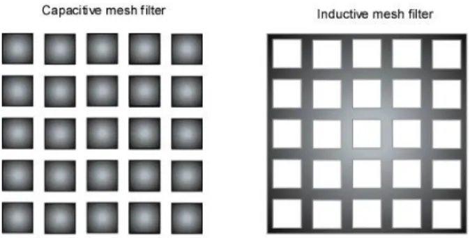
Frequency selective surfaces are printed bidimensional periodic structures able to filter electromagnetic signals with different characteristic depending on geometry, repetition period of unit cells and on the characteristic of surrounding dielectric layers [20]. Frequency selective surfaces are commonly separated in capacitive or inductive geometries if they are realized by repeating a metallic unit cell or if they are composed by periodic holes in a metal plate respectively. An inductive FSS operates like a pass‐ band filter, whereas a capacitive FSS behaves similarly to a stop‐band filter.
Frequency selective surfaces, differently from high impedance surfaces, have a long history and their properties have been largely investigated by researchers [21]‐[49]. For this reason, particular attention is dedicated to a review of the material currently available on this topic. Subsequently an equivalent circuit method for modeling the response of such periodic filter is proposed [50], [51].
1.2 Frequency Selective Surfaces 3
Fig. 1.2 ‐ Layout of capacitive and inductive frequency selective surfaces and their equivalent circuit
representation.
1.2.1 FSS model
A circuit approach for the analysis of frequency selective surfaces is proposed. The analysis is based on the hypothesis that the response of a single resonant FSS element can be represented by a simple series or parallel LC circuit if the FSS is respectively capacitive or inductive. After a single full‐wave simulation, it is possible to obtain the impedance of the freestanding FSS and then calculating the values of the equivalent capacitances and inductances. In absence of losses the FSS impedance results purely imaginary while in presence of losses a series resistance is added in the circuit. The design parameters such as repetition period of the unit cell, angle of incidence of the impinging wave, properties of the supporting dielectric layers influence the values of the computed FSS inductances and capacitances and, for this reason, the model here presented introduces simple relations that matches the mentioned variations. Differently from other approaches, the circuit model here proposed is valid for every kind of FSS element and in presence of thin supporting dielectrics.
1.3 HighImpedance Surfaces
The circuit analysis of the FSS, providing good physical insights into the design properties of the electromagnetic structure, results of vital importance in the analysis of high‐impedance surfaces. By means of the equivalent transmission line approach, the general theory of high‐impedance surfaces and their properties in presence of surface waves are presented in the third chapter [1]‐[16]. As is well known, a high‐
4 Chapter 1 – Introduction and Outline impedance surface can be interpreted as a reactive surface whose input impedance is equal to the parallel connection of the capacitive impedance given by the frequency selective surface and the inductive impedance of a grounded dielectric slab. This parallel connection generates a distributed resonant circuit that creates, at the resonance, a high inductive input impedance in a reduced thickness. For an impinging plane wave, this surface mimics the Perfect Magnetic boundary condition (PMC) within a small frequency range and, for this reason, it is often referred to as Artificial Magnetic Conductors (AMC). It is therefore evident that the bandwidth of this metasurface is one of the key feature of the structure. Even if these surfaces have been employed for almost ten years, it is sometimes unclear how to choose the shape of the frequency selective surface on the top of the grounded slab in order to achieve the largest possible bandwidth.
1.3.1 Analysis of HIS Bandwidth
The issue of the bandwidth of high‐impedance surfaces is treated in the third chapter through a transmission line analysis [17] based on the circuit representation of the FSS previously described. It is shown that the conventional approach that approximates the high‐impedance surface as a parallel connection between the inductance given by the grounded dielectric substrate and the capacitance of the FSS may induce inaccurate results in the determination of the operating bandwidth of the structure. Indeed, in order to derive a more complete model and to provide a more accurate estimate of the operating bandwidth, it is also necessary to consider the series inductance of the FSS. The explicit expression for defining the bandwidth of a high‐impedance surface is obtained and it is shown that the reduction of the FSS inductance results the best choice for achieving wide operating bandwidth in correspondence of a given frequency.
1.4 Applications: Electromagnetic Absorbers
As mentioned above, the peculiar properties characterizing a high‐impedance surface, allow to employ the surface in different application in microwave area. Based on the theoretical analysis introduced in the two initial chapters, the thesis analyzes the
1.4 Applications: Electromagnetic Absorbers 5 application of HIS in the design of electromagnetic absorbers [52]‐[90]. In the last years, high‐impedance surfaces have been employed to improve the performances of the classical electromagnetic absorbing structures [70]‐[90]. Thin narrow band absorbers employing metallic FSS loaded with a large number of lumped resistors have been repeatedly proposed [75]‐[80]. Loaded HIS surfaces can be also employed to synthesize thin and wideband absorbers [81]‐[86]. Here, resistive frequency selective surfaces are employed to synthesize the absorber [87], [88]. A theoretic discussion about the absorbing principle is presented through a circuit model. Moreover a methodology to enhance the absorption properties of the thin narrow‐ band absorbers at oblique incidence is then presented and discussed [89], [90]. Finally high‐impedance surfaces are used to replace the perfect electric backing plane of the classical Salisbury screen absorber [72], [73].
1.4.1 Thin absorbers based on resistively loaded HIS
The absorber comprises a resistively loaded high‐impedance surface [87]. Losses in the structure are introduced by printing the periodic pattern through resistive inks and hence avoiding the typical soldering of a large number of lumped resistors. The novel absorber can be employed for synthesizing both thin narrowband and wideband absorbers that strongly outperform the conventional Salisbury and Jaumann configurations. The use of resistive patterns provides a dramatically simpler, more lightweight and cheaper structure with respect to the classical design. Both a theoretical discussion and practical realizations of the structure are reported. The effect of the surface resistance of the FSS and dielectric substrate characteristics on the input impedance of the absorber is discussed by means of a circuit model. It is shown that the optimum value of surface resistance is affected both by substrate parameters (thickness and permittivity) and by FSS element shape. By the equivalent circuit model, the working principles of both narrowband and wideband absorbing structures are addressed and the best‐suited FSS element for achieving the most wideband absorption is derived. Finally, practical designs of the thin absorbing structures and their experimental validation are presented. A 3D sketch of the absorbing structure is reported in Fig. 1.3.
6 Chapter 1 – Introduction and Outline
Fig. 1.3 Layout of the absorbing structure based on resistive frequency selective surfaces.
The theory of ultra‐thin narrow band absorbers is also treated by a transmission line model based on an averaged approximation of the frequency selective surface [89]. The analysis methodology works pretty well when the FSS is composed by an array of patches with a repetition period sufficiently smaller than the wavelength and it allows also to model the presence of metal connection between the patch array and the ground plane. The array of wires, generated by the presence of periodic vias in the HIS, can be modeled through the quasi‐static theory of wire medium since the presence of the FSS on the top of the wires avoids the spatial dispersion in the wire array [12]. The wire medium introduces a plasma resonance [144] in the HIS response and it can be exploited to enhance the performance of practical devices as for instance electromagnetic absorbing materials. It is shown that the presence of the vias influences the oblique incidence TM absorption, and when properly designed, it results in a bandwidth enlargement and higher absorption performance. A layout of the absorbing structure is shown in Fig. 1.4.
Fig. 1.4 – Layout of the oblique incident improved absorbing structure.
1.4.2 Salisbury screen with reactive ground plane
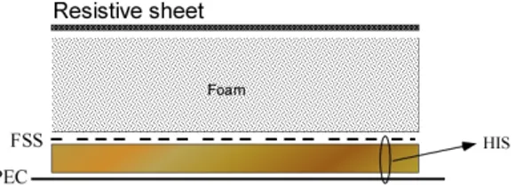
A further interesting application of high‐impedance surfaces as backing plane in conventional Salisbury‐type electromagnetic absorbers is described [72], [73]. The
1.4 Applications: Electromagnetic Absorbers 7 novel design comprises a single resistive sheet mounted at a fixed distance from a reactive HIS structure. The high‐impedance surface acts as an artificial magnetic conductor at lower frequencies, while responding as a perfect electric conductor at higher frequencies. The presence of the new ground plane allows to recover the Salisbury functions in the upper band, while operating as a λ/10 absorber in the low frequency regime. When the high‐impedance surface acts as a PEC plane, the Salisbury screen works in the conventional way. Conversely, when the composite layer (composed by the first grounded dielectric layer, the FSS and the second dielectric) behaves as a high‐impedance surface the resistive sheet is again mounted over a magnetic wall and it causes an additional resonant absorption peak. A layout of the absorbing structure is shown in Fig. 1.5.
Fig. 1.5 – Layout of the absorbing structure based on reactive ground plane.
1.5 Applications: Antennas
The two final chapters of the thesis are focalized on the use of high‐impedance surfaces in the design of two different types of antenna. The former design is composed by an horizontal small dipole antenna placed in close proximity of a high‐ impedance surface [1]. In this design, the use of high‐impedance surfaces allows to overcome the fundamental limitation concerning the distance between the antenna and the ground plane imposed by horizontal wire antennas over an electric ground plane. The optimal distance for the antenna on the PEC is in fact a quarter wavelength, high radiation resistance being the figure of merit. If the separation is reduced, the image currents on the ground plane eventually cancel out all radiation from the antenna. A sketch of the dipole antenna on the top of the high‐impedance surface is reported in Fig. 1.6. The thesis investigates both theoretically and from a practical
8 Chapter 1 – Introduction and Outline point of view the properties of such antennas. Despite the large amount of work published on this topic [91]‐[101], the theory of such device is still unclear. Simple image principles, based on a schematization of the HIS as a perfect magnetic conductor, are often used both to explain and model the structure. The reflection phase of infinite high‐impedance surface at normal incidence is also often employed in modelization tools that neglects both the strong angular dependence of HIS input impedance and the finite size of a real structure.
Fig. 1.6 – Layout of the analyzed antenna.
In the latter case, high‐impedance surfaces are employed in the design of the so‐called Fabry‐Perot or Leaky wave antennas [104]‐[118]. Fabry‐Perot antennas have been presented in literature by Trentini in 1956 but their performance have been improved in the last five years with the use of high‐impedance surfaces [104]. A Fabry‐Perot antenna is usually realized by placing a highly reflective dielectric or a frequency selective surface at a proper distance from a ground plane [105]. The cavity, excited by a low gain antenna, transforms an omnidirectional field distribution into a highly directive one. In the case of a metallic ground plane, the cavity height equals λ/2. Fig. 1.7 – Layout of the high directive sub‐wavelength Fabry‐Perot antenna. However, it has been demonstrated that when the metallic plate is replaced by a high‐ impedance surface, the reflection phase of this ground plane can be properly chosen
1.5 Applications: Antennas 9 leading to a sub‐wavelength design [122]‐[125]. A sketch of the Fabry‐Perot antenna with the HIS structure in place of an electric ground plane is reported in Fig. 1.7.
1.5.1 Lowprofile antennas
It is shown in the thesis that a finite antenna system is characterized by two radiating mechanisms: the first one is the classical resonance of the HIS‐based antenna system, and the second one is due to the propagation of TE surface waves in a finite structure [102]. The propagation of TE surface waves cause additional resonances on the s11 profile dependent on the size of the HIS structure. Depending on the size of the HIS, these resonances can be exploited to widen the operating band of the antenna. The dimension of the backing plane is of crucial importance on the radiation properties of the antenna and it is demonstrated which is the actual relation between the radiation pattern of the antenna and the size of the high‐impedance surface. The shape of the radiation patterns of the antenna is analyzed both before the HIS resonance and in the range where TE surface wave are propagating. Before the HIS resonance, the only propagating surface wave results a TM wave and it is demonstrated that the shape of the radiation patterns is univocally determined by the size of the structure [103]. The introduction of the frequency selective surface leads to a HIS resonance in the input impedance resulting in the antenna matching and in the onset of TE surface waves after the mentioned resonance. It is shown that the shape of the radiation patterns, independently of the FSS unit element shape, remains rotationally symmetric and wide‐beam up to the first TE surface wave resonance and it deteriorates after that. The presence of vias in the HIS is also analyzed. It is commonly accepted that the use of EBG materials prevents the diffraction of surface waves at the edges of the finite structure reducing the grazing radiation, the back radiation (or the front to back ratio) and the coupling with other antennas. Here it is shown that the presence of vias in the high‐impedance surface, that allows to block the propagation of surface waves, does not improve the goodness of the radiation pattern and deteriorates the matching of the radiating element. The theoretical analysis of the low‐profile antenna is supported by experimental validations on ad‐hoc prototypes.The modeling of the low‐profile antenna is finally addressed. A benchmark antenna structure is analyzed by a full‐wave code and the results are compared with numerical
10 Chapter 1 – Introduction and Outline simulations of the same antenna in which the actual finite‐size high‐impedance surface is replaced by an impedance boundary of the same size. The surface impedance of the boundary is either defined assuming plane‐wave normal incidence or considering a partially homogenized structure composed by a grounded dielectric slab and a homogenized layer representing the frequency selective surface on top of the slab. It is demonstrated that, even if the accuracy of the model can be gradually improved, the use of homogenized approach to analyze an horizontal dipole on a high‐ impedance surface does not guarantee acceptable accuracy. A further improvement of a high‐impedance surface consists in apply varicap diodes in every unit cell of the FSS for tuning its high‐impedance condition. This technique is here used to design a prototype of a tunable antenna [95].