Nanotechnology
PAPER • OPEN ACCESS
Surface properties of SnO
2
nanolayers prepared by spin-coating and
thermal oxidation
To cite this article: M Kwoka et al 2020 Nanotechnology 31 315714
View the article online for updates and enhancements.
Surface properties of SnO
2
nanolayers
prepared by spin-coating and thermal
oxidation
M Kwoka
1, B Lyson-Sypien
1, E Comini
2, M Krzywiecki
3,
K Waczynski
4and J Szuber
11
Department of Cybernetics, Nanotechnology and Data Processing, Faculty of Automatic Control, Electronics and Computer Science, Silesian University of Technology, 44-100 Gliwice, Poland
2
SENSOR Lab, Department of Information Engineering(DII), Brescia University, 25123 Brescia, Italy
3Institute of Physics—Center for Science and Education, Silesian University of Technology, 44-100
Gliwice, Poland
4
Department of Electronics, Electrical Engineering and Microelectronics, Faculty of Automatic Control, Electronics and Computer Science, Silesian University of Technology, 44-100 Gliwice, Poland E-mail:[email protected]
Received 13 October 2019, revised 13 January 2020 Accepted for publication 12 February 2020
Published 20 May 2020 Abstract
In this work, comparative studies of the surface morphology and surface chemistry of SnO2 nanolayers prepared by spin coating with subsequent thermal oxidation(SCTO) in the temperature range of 400–700 °C using scanning electron microscopy (SEM), atomic force microscopy (AFM) and x-ray photoelectron spectroscopy(XPS) methods, are presented. The SEM images show that SCTO SnO2nanolayers contain partly connected irregular structures strongly dependent on the final oxidation temperature, with interconnected single grains of longitudinal shape and size, resulting in aflatter surface morphology with respect to the commonly used three-dimensional (3D) SnO2thinfilms. In turn, AFM studies additionally confirm that SCTO SnO2nanolayers after post-oxidation annealing at higher temperatures contain isolated grains of average lateral dimensions in the range of 20–50 nm having a rather flat surface morphology of average surface roughness defined by the root mean square factor at the level of ∼2 nm. From the XPS experimental research it can be concluded that, for our SCTO SnO2samples, a slight surface nonstoichiometry defined by the relative [O]/[Sn] concentration at the level of 1.8–1.9 is observed, also depending on thefinal post-oxidation temperature, being an evident contradiction to recently published literature using x-ray diffraction data. Moreover, XPS experiments show that there is also a permanent small amount of carbon contamination present at the surface of internal grains of our SCTO SnO2nanolayers, creating an undesired potential barrier for interactions with gaseous species when they are used as the active materials for gas sensing devices.
Keywords: tin dioxide SnO2nanolayers, spin coating technology, surface morphology, SEM, AFM, surface chemistry, XPS
(Some figures may appear in colour only in the online journal)
Introduction
Tin dioxide(SnO2) is a wide band gap (3.6 eV) n-type semi-conductor with a rutile structure[1] that has fascinating
phy-sicochemical properties including, among others, a high electrical conductivity (∼102 W−1×cm−1) with the natural
Nanotechnology 31(2020) 315714 (7pp) https://doi.org/10.1088/1361-6528/ab7586
Original content from this work may be used under the terms of the Creative Commons Attribution 4.0 licence. Any further distribution of this work must maintain attribution to the author(s) and the title of the work, journal citation and DOI.
tendency to variability after exposure to various gases[2, 3].
This is why SnO2, mainly in the form of thick and thinfilms, has been applied in resistivity-type gas sensor devices[4,5] for
environmental and medical applications[6].
In the last decade, research has been focusing on low dimensional SnO2 nanostructures, including among others nanowires and nanobelts, due to their enlarged surface-to-volume ratio as well as enhanced chemical stability and electrical performance[7,8]. However, thin film technology
is a core high-yield fabrication method for real-world sensors because of its main advantages such as low power con-sumption. There are various physical and chemical techniques that have been implemented recently for the preparation of SnO2 thin films, which were comprehensively reviewed in [5,6]. Depending on the deposition method, post annealing or
manipulation of the substrate temperature and gas pressure can be used to control the size of the crystallites and to intentionally obtain the desired and optimized morphology. This is extremely important as the shape and size of SnO2 nanostructures have a significant influence on their gas sen-sing properties[9,10].
Within the physical deposition methods, a great tendency has appeared in the last several years towards developing lower temperature and inexpensive methods for deposition of SnO2 nanostructured thinfilms. Apart from the well-known sol–gel (SG) [11] and spray pirolysis (SP) [12] methods, one
of the most promising low temperature technologies for preparation of SnO2nanolayers is a method of spin coating deposition of specific precursors on Si substrate proposed by Cukrov et al [13] and then further developed by Bazargan
et al[14], Khuspe et al [15] and Uysala et al [16].
Bazargan et al [14] recently observed that using the
SnCl4 solution and performing spin-coating deposition on etched glass substrates combined with post-deposition annealing(oxidation) in an oxygen atmosphere in the temp-erature range of 350–500 °C resulted in the formation of uniform, flat granular SnO2 thin films containing mono-disperse crystallites with sizes in the range of 7–10 nm and having a low root mean square (RMS) surface roughness (1.6–2.2 nm). Moreover, it was observed that after post-annealing in an oxygen atmosphere at temperatures above 500°C the surface roughness increased since the RMS factor was evidently higher (∼6), whereas the dimensions of the more isolated crystallites increased up to∼25 nm.
In turn, Khuspe et al[15] combined the sol-gel technique
for the preparation of homogeneous solution containing SnO2powder with its subsequent spin coating deposition on glass substrate for the preparation of SnO2 nanostructured thin films also containing tetragonal nanocrystallites with dimensions in the range of 5–10 nm for NO2 gas sensing application.
A similar sol-gel spin coating deposition procedure combined with additional post-annealing in air in the temp-erature range 450–650 °C was applied by Uysala et al [16] for
the preparation of SnO2nanostructured thinfilms for potential photovoltaic applications.
However, it can be noticed that the issue of the local surface chemistry of SnO2 nanolayers (namely the surface
nonstoichiometry together with undesired carbon C con-tamination commonly adsorbed at the surface of various SnO2 forms from the air atmosphere), has been rather neglected in the literature undertaking the subject of spin coated SnO2and listed above. This is of great importance for SnO2gas sensor performance, mainly for the gas sensitivity as well gas sensor aging effects, as observed in our recent studies of L-CVD SnO2nanolayers[17] and PVD SnO2nanowires[18].
Driven by these facts, in our last studies we have focused on the surface impact on the properties of SnO2 nanolayers deposited by spin-coating and subsequent thermal oxidation (SCTO) based on the systematic comparative scanning elec-tron microscopy(SEM) and atomic force microscopy (AFM) studies of their surface morphology, including grain dimen-sion and roughness, combined with the x-ray photoelectron spectroscopy(XPS) studies of their surface chemistry (purity and stoichiometry) in view of their potential application in novel types of conductometric gas sensor devices.
Experimental
The SnO2nanolayers used in our studies have been deposited by the spin-coating method using SnCl4·5H2O in isopropanol at the rotation speed of 1800 rpm on Si(111) substrate recently cleaned (etched) in HCl solution in order to remove the natural oxide and then covered with an approximately 8 nm Aufilm to improve the stability, adhesion to substrate and deposited thin film homogeneity. At the second step, after a short period of drying in dry air at 100°C, an additional thermal oxidation of the above mentioned deposited layer was performed for 1 h at various temperatures in the range of 400–700 °C in a dry air atmosphere inside a reaction chamber of a typical diffusion furnace. The thickness of our SCTO SnO2 was estimated to be about ∼200 nm, and does not significantly evolve during above mentioned post-oxidation procedure. Other experimental details can be found in[19].
The local surface morphology of our SCTO SnO2 sam-ples was controlled using the SEM method at Brescia Uni-versity (Italy), with a Zeiss LEO 1530 Model SEM microscope. More experimental details regarding this method can be found in[18]. For a more quantitative analysis of the
surface morphology of our SCTO SnO2samples including the shape of individual grains, the AFM method was additionally applied using the XE-70 Park model working in a non-contact mode. In turn, the surface chemistry of SCTO SnO2thinfilms was controlled by the XPS method using the SPECS XPS spectrometer equipped with x-ray Al Kα source at photon energy 1486,6 eV (XR-50 model, and a concentric hemi-spherical analyzer (CHA PHOIBOS 100 model). Other experimental details can be found elsewhere in[17,18].
Results and discussion
SEM and AFM investigations of SCTO SnO2 thin films showed that their extremely complex morphological land-scape is strongly dependent on the temperature of thermal
2
post-oxidation during the second step of the preparation procedure.
The respective SEM images of our SCTO SnO2 nano-layers post-oxidized(annealed) at various temperatures in the range of 400–700 °C are shown in figure1.
From the respective SEM images one can observe, that for the lower post-oxidation temperatures (below 500 °C) SCTO SnO2nanolayers exhibit evidently continuous surface morphology, as observed recently by Bazargan et al [14],
without visible single crystalline forms.
What is the most important, as our SEM studies confirmed, SCTO SnO2 nanolayers after post-oxidation at temperatures higher than 500°C exhibit a well separated grain structure. In our previous paper[19], undertaking XRD phase analysis of SCTO
SnO2nanolayers, it was shown that the samples demonstrated an irregular crystalline structure on the(110) facets and the Debye– Scherrer formula showed that the average sizes of the inter-connected individual grain-type SnO2 crystallites in the SCTO SnO2nanolayers after post-oxidation at temperatures of 500 and 700°C were 5.1 and 6.7 nm, respectively.
In addition to the above, for the SCTO SnO2nanolayers after post-oxidation at the highest temperature of 700°C, one can observe from the respective SEM image that the grain’s shape becomes more longitudinal as the average width and length of a single grain are at the level of∼20 nm and 50 nm, respectively. In relation to the above, it appears that our results of SEM characterization slightly differ from the SEM experiments of Bazargan et al [14], who observed almost
isolated crystalline grains of the average lateral dimension ∼25 nm. However, there are several reasons for these dif-ferences beginning with the temperature range of the post-oxidation procedure, the various lateral resolutions of respective SEM images, different surface preparation proce-dures of the Si substrate, various oxidizing atmospheres of the post-oxidation procedure andfinally the respective flow rates. As was mentioned above, for additional verification of the shape of individual grains of our SCTO SnO2nanolayers, AFM comparative studies were additionally performed. Figure 2 shows the 3D AFM image of the internal, local structure of a SCTO SnO2nanolayer after post-oxidation at the highest temperature of 700°C, together with the corresponding AFM profile.
As can be seen, the AFM experiments confirm that the nanograins of the formed SCTO SnO2 nanolayers are more longitudinal with respect to the experiments of Bazargan et al [14] with an average maximum height below 10 nm, and
average lateral dimension in the range of 20–50 nm. However, at the same time, one can conclude that AFM imaging in the case of the presented SnO2nanolayers is mod-erately corrugated, which can be related to the influence of the tip convolution to a large extent. Moreover, the discussed SCTO SnO2nanolayers are ratherflat as in our case the RMS factor, being the measure of the average surface roughness is at the level of∼2 nm being evidently smaller (∼3 times) than the one presented by Bazargan et al[14]. The above conclusion that our
SCTO SnO2nanolayers exhibit a veryflat surface morphology in comparison to the commonly used SnO2 thin films, as reviewed by Eranna[7], is of great importance from the point of
view of possible applications in photovoltaics as transparent conductive electrodes. Furthermore, it should be emphasized that our SCTO SnO2 nanolayers after post-oxidation at Figure 1.SEM images of SCTO SnO2nanolayers for different
temperatures higher than 500°C contain irregular but isolated grains of average lateral dimension not far from the Debye length(∼several nm), for which the highest sensitivity of metal oxide gas sensor materials are commonly observed[7,8]. From
this point of view the SCTO SnO2nanolayers would be highly promising candidates for potential gas sensing applications.
In parallel to the surface morphology, in this subsection the main results of the XPS studies of SCTO SnO2nanolayers after deposition are presented and analyzed.
For all the XPS survey spectra of SCTO SnO2nanolayers for different oxidation temperatures in the rangeof 500–700 °C, which looked very similar, the contribution of the main O1s, single peaks, and the double Sn3d3/2 and Sn3d5/2 peaks corresponding to the two main elements were observed.
Moreover, for all XPS survey spectra, an evident contribution of single XPS C1s peak was also observed, that confirmed the existence of carbon C surface contamination on the surface of our SCTO SnO2nanolayers.
For a more precise analysis of the surface chemistry of our SCTO SnO2samples, including their stoichiometry, the core level XPS O1s-Sn3d spectral windows were used, shown infigure3. Taking into account the area under the principal components of XPS O1s and Sn3d5/2 peaks and using the analytical procedure based on the atomic sensitivity factor (ASF) [20], the relative [O/Sn] atomic concentration was
determined. A similar procedure based on XPS survey spectra
in the binding energy range of 600–0 eV (not presented here) and the area under the respective principal components of C1s and Sn3d5/2was used in the determination of relative[C/Sn] atomic concentration. The obtained results for all our SCTO SnO2samples are summarized in table1.
As shown in table1, the XPS experiments confirm that the surface of all our SCTO SnO2 nanolayers is slightly non-stoichiometric, with an evident domination of tin dioxide which is crucial, and we have to underline at this point, is that the above conclusion cannot be understood as contradictory to information obtained from our previous XRD experiments[19].
Figure 2.3D AFM image of the internal, local structure of SCTO SnO2nanolayer, together with the corresponding AFM profile.
Figure 3.XPS O1s-Sn3d spectral windows of SCTO SnO2
nanolayers for different post-oxidation temperature.
Table 1.Relative surface concentrations of O and Sn basic elements in SCTO SnO2nanolayers including C contamination for the
different post-oxidation temperatures.
Relative concentration Temperature of post-oxidation of
SCTO SnO2nanolayers[°C] O/Sn C/Sn
500 1.80±0.05 2.65±0.08
600 1.85±0.05 1.90±0.08
700 1.90±0.05 1.00±0.08
4
The XRD results presented in[19] clearly indicated only
the presence of SnO2formed in the SCTO SnO2nanolayers under study. However, in contrast to the XRD method, one has to bear in mind that XPS is primarily a surface sensitive technique, especially when using the x-ray photon energy (1486.6 eV), able to recognize the surface chemical species in the veryfirst few layers in depth only up to 10 nm. This is why the XPS method was used in our studies for the deter-mination of effective surface nonstoichiometry of SCTO SnO2nanolayers, which is extremely important regarding the value of the Debye length for SnO2 at the level of several nm[5,7].
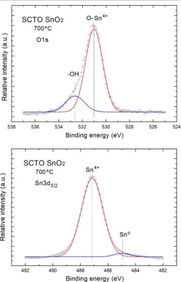
In order to prove the above statement, the decomposition of XPS O1s and Sn3d5/2 peaks for the sample with the highest[O]/[Sn] relative concentration was performed, as can be seen infigure4.
Concerning the XPS O1s line(figure 4), a simple visual
shape confirms that it is wide, asymmetrical and exhibits an evident shoulder at the higher binding energy side of the spectrum. After decomposition (deconvolution) using the fitting procedure with the Gaussian distributions, it becomes evident that it contains two components separated by 1.4 eV
corresponding to O atoms (ions) in bonding with various surface atoms(ions). The main parameters used in the applied fitting procedure, as well as the obtained best fitting para-meters are summarized in table 2.
The XPS O1s line component at lower binding energy (531.0 eV) corresponds to O2ions in the Sn–O band (named lattice oxygen), whereas the second one at higher binding energy(532.4 eV) can be attributed to hydroxyl groups (H–O band) adsorbed at the surface. Their relative area (intensity) is at the level of∼1.8. This is important, similar XPS O1s line components were recently observed by Mazloom et al [21]
for Co-doped SnO2thinfilms, also prepared using the sol–gel spin coating technique.
Concerning the XPS Sn3d5/2 line (figure 4), a simple visual shape analysis also confirms that it is wide, slightly asymmetrical and exhibits a small shoulder at the lower binding energy side of the spectrum. After decomposition (deconvolution) using fitting with Gaussian distributions, it is evident that it contains two components separated by 2.3 eV corresponding to Sn atoms (ions) bonding with various sur-face atoms (ions). The main parameters used in the fitting procedure, as well as the obtained fitting parameters are also summarized in table 2.
The main component of XPS Sn3d5/2 line at higher binding energy of 471.2 eV corresponds to Sn4+ions in Sn–O band(lattice oxygen), whereas the second one (very small) at lower binding energy (∼485.0 eV) can be attributed to the existence of Sno bondings related to the small amount of metallic Sn. Their relative area (intensity) is in good agree-ment with the information on relative concentration[O]/[Sn] ratios obtained from the O1s-Sn3d spectral windows that the SCTO SnO2 nanolayers under the last analysis are only slightly nonstoichiometric, with an evident domination of tin dioxide SnO2. Similar XPS O1s line components were also observed in our recent studies of RGVO SnO2 nano-layers[22].
As was mentioned earlier, the main difference in the surface chemistry of our SCTO SnO2nanolayers, observed in the XPS survey spectra, is the amount of C contaminations.
In general, they come from the different C gaseous species present in the natural air atmosphere, which imme-diately adsorb at the surface of all semiconductor materials (time ∼ms) and are controlled by the mass spectrometry (MS). The relative [C]/[Sn] concentration at the surface of our SCTO SnO2 nanolayers evidently depends on the post-oxidation temperature, as summarized in table1.
Figure 4.Decomposed XPS O1s and Sn3d5/2peaks of SCTO SnO2
nanolayers having the highest[O]/[Sn] relative concentration.
Table 2.The binding energy, full width at half maximum(FWHM) and relative surface area of main components of XPS Sn3d5/2and O1s peaks after their decomposition for SCTO SnO2nanolayers.
XPS peak parameters O1s Sn 3d5/2
Components OH– O–Sn4+ Sno Sn4+
Binding energy[eV] 532.4 531.0 485.0 487.2
FWHM[eV] 2.21 1.43 1.12 1.56
For the samples after post-oxidation at the lowest temp-erature of 500°C it is at the level of 2.65, slightly lower than for the freshly deposited L-CVD SnO2 thin films after air exposure observed in our recent studies[23–25]. In turn, for
the SCTO SnO2nanolayers after post-oxidation at the highest temperature of 700°C it is almost three times lower. This is probably related to the fact that they exhibit more tight (packaged) surface morphology corresponding to the greater dimensions of the interconnected individual nanograins and then the respective smaller channels between them are usually ‘open’ for potential undesired diffusion of C contaminations (mainly as CO2) from the residual gas atmosphere. Crucially, the average distances between the nanograins in our SCTO SnO2 nanolayers are evidently smaller with respect to the most‘open’ surface observed for the L-CVD SnO2thinfilms, as well as the SnO2 thin films obtained by the rheotaxial growth and thermal oxidation (RGTO) in our recent studies [26]. Importantly, those C contaminations at the surface of
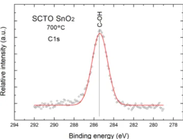
our SCTO SnO2nanolayers are in the form of C–OH bond-ing, as it was recognized after decomposition of XPS C1s peak shown infigure5.
The same shape of this XPS C1s peak was observed for all the samples under our studies.
Already a simple visual shape analysis also confirms that it is wide and symmetrical.
After decomposition (deconvolution) of the XPS C1s peak using fitting with Gaussian distributions, it is evident that it contains only one component at the binding energy 285.5 eV, that can be attributed to the C-OH surface bonding commonly observed at various semiconductor surfaces including oxides[1,20,27]. Unfortunately, the undesired fast
C adsorption on the surface of SnO2nanolayers (grains) is extremely critical for their gas sensor application because it strongly affects the response time of gas sensor devices. This is because every active(toxic) gas has to flow towards the gas sensitive active centers, for instance SnO2 nanolayers, through the C contamination (up to ∼3 atomic layers in average), which generates an undesired and uncontrolled barrier for potential toxic gas adsorption at the internal surface of the sensor material.
Conclusions
In this paper the results of comparative studies of the surface morphology and surface chemistry of SCTO SnO2 nano-layers using a combination of SEM, AFM and XPS methods are presented. SEM and AFM studies show that the specific surface morphology of SCTO SnO2 nanolayers exhibit partly connected irregular structures with interconnected single grains of more longitudinal shape and size, resulting inflatter morphology corresponding to an average roughness (RMS) below 2 nm, as derived from the AFM studies, being very promising for their potential photovoltaic appli-cations as transparent conductive electrodes. Moreover, SCTO SnO2thinfilms contain almost isolated longitudinal grains of average width and length at the level of∼20 nm and 50 nm, respectively, not so far from the Debye length (∼several nm). From this point of view, they can be con-sidered as a promising novel form of metal oxide material for potential applications in novel types of conductometric gas sensors.
In turn, XPS studies confirm that for SCTO SnO2 sam-ples, a slight surface nonstoichiometry at the level of 1.8–1.9 is observed, together with C contamination, probably at the surface of internal grains. This undesired effect cannot be ignored because it generates an uncontrolled barrier for the potential adsorption of interacting gases at the internal surface of the sensor material. This is why, this undesired and uncontrolled C contamination at the internal surface of SCTO SnO2thin films appears to be the most important limitation for application in novel sensor devices. In relation to this, an understanding of the adsorption/desorption behavior of C contamination at the surface of SCTO SnO2 nanolayers is crucial for the interpretation of the gas sensing mechanism. Such studies, also in comparison to the various 1D forms of SnO2, including nanowires and nanobelts, are currently in progress in our labs.
Acknowledgments
The authors are grateful to Natalia Waczynska-Niemiec for helping K W to prepare SCTO SnO2nanolayers within the Network Project InTechFun founded by the Operational Programme of Innovation Economy: UDA-POIG.01.03.01-00-159/08. This work was realized within the subsidy for maintaining and developing the research potential of Department of Cybernetics, Nanotechnology and Data Pro-cessing, Silesian University of Technology, Gliwice, Poland. The work of the authors M K, M K and J S has been sup-ported by the research grant of National Science Centre, Poland - OPUS11, 2016/21/B/ST7/02244. M K and B L-S additionally would like to acknowledge the funding of Pro-fessor Grant (GP) of the Silesian University of Technology no. 02/030/RGP19/0050 and the research grant of Polish National Centre of Science - 2016/20/S/ST5/00165, respectively.
Figure 5.Decomposed XPS C1s peak of SCTO SnO2nanolayers.
6
ORCID iDs M Kwoka https://orcid.org/0000-0001-6197-1191 B Lyson-Sypien https://orcid.org/0000-0001-6019-7835 M Krzywiecki https://orcid.org/0000-0002-6151-8810 J Szuber https://orcid.org/0000-0002-7012-8224 References
[1] Batzill M and Diebold U 2005 Prog. Surf. Sci.79 47
[2] Göpel W and Schierbaum K-D 1995 Sensors and Actuators B
26 27
[3] Barsan N, Schweitzer-Barberich M and Göpel W 1999 J. Anal. Chem.365 287
[4] Ihokura K and Watson J 1994 The Stannic Oxide Gas Sensor: Principles and Applications(Boca Raton USA: CRC Press) [5] Comini E et al (ed) 2009 Electrical based gas sensors Solid
State Gas Sensing(New York: Springer)p 47
[6] Barsan N, Koziej D and Weimar U 2007 Sensors and Actuators B121 18
[7] Eranna G 2012 Metal Oxide Nanostructures as Gas Sensing Devices(Boca Raton USA: CRC Press)
[8] Carpenter M A, Mathur S and Kolmakov A 2012 Metal Oxide Nanomaterials for Chemical Sensors(New York USA: Springer)
[9] Yamazoe N 1991 Sensors and Actuators B5 7
[10] Bose C, Thangadurai P and Ramasamy S 2006 Materials Chemistry and Physics95 72
[11] Shukla S, Patil S, Kuiry S C, Rahman Z, Du T, Ludwig L, Parish C and Seal S 2003 Sensors and ActuatorsB96
343
[12] Brinzari V, Korotcenkov G and Golovanov V 2001 Thin Solid Films391 167
[13] Cukrov I M, Mc Cormick P G, Galatsis K and Wlodarski W 2001 Sensors and Actuators B77 491
[14] Bazargan S, Heinig N F, Pradhan D and Leung K T 2011 Cryst. Growth Design11 247
[15] Khuspe G D, Sakhare R D, Navale S T, Chougule M A, Kolekar Y D, Mulik R N, Pawar R C, Lee C S and Patil V B 2013 Ceramics Int.39 8673
[16] Uysala B Ö, Özlem Ü and Arıer A 2015 Applied Surface Science350 74
[17] Kwoka M, Ottaviano L, Koscielniak P and Szuber J 2014 Nanoscale Research Letters9 260
[18] Sitarz M, Kwoka M, Comini E, Zappa D and Szuber J 2014 Nanoscale Research Letters9 43
[19] Izydorczyk W, Waczynski K, Izydorczyk J, Karasinski P, Mazurkiewicz J, Magnuski M, Uljanow J,
Waczynska-Niemiec N and Filipowski W 2014 Materials Science(Poland)32 729
[20] Moulder J F, Stickle W F, Sool P E and Bomben K D 1992 Handbook of X-ray Photoelectron Spectroscopy(USA: Perkin-Elmer Eden Prairie)
[21] Mazloom J and Ghodsi F E 2013 Materials Research Bulletin
48 1468
[22] Kwoka M and Krzywiecki M 2015 Materials Letters154 1
[23] Kwoka M, Ottaviano L, Passacantando M, Santucci S, Czempik and Szuber J 2005 Thin Solid Films490 36 [24] Kwoka M, Ottaviano L, Passacantando M, Santucci S and
Szuber J 2006 Applied Surface Science252 7730 [25] Kwoka M, Waczynska N, Kościelniak P, Sitarz M and
Szuber J 2011 Thin Solid Films520 913
[26] Ottaviano L, Kwoka M, Bisti F, Parisse P, Grossi V, Santucci S and Szuber J 2009 Thin Solid Films517 6161 [27] Atashbar M Z, Sun H T, Gong B, Wlodarski W and Lamb R