OLED devices optimization for
lighting application
Salvatore Aprano
Unione Europea UNIVERSITÀ DEGLI STUDI DI SALERNO
FONDO SOCIALE EUROPEO
Programma Operativo Nazionale 2000/2006
“Ricerca Scientifica, Sviluppo Tecnologico, Alta Formazione” Regioni dell’Obiettivo 1 – Misura III.4
“Formazione superiore ed universitaria”
Department of Industrial Engineering
Ph.D. Course in Electronic Engineering
(XV Cycle-New Series, XXIX Cycle)
OLED devices optimization for lighting
application
Supervisor
Ph.D. student
Prof. Alfredo Rubino
Salvatore Aprano
Dott.sa Maria Grazia Maglione
Scientific Referees
Prof. Alessandro Pezzella
Dott. Mario Barra
Ph.D. Course Coordinator
“It is during our darkest moments
that we must focus to see
the light.”
-Alexander Onassis-
Scientific Works
• "Eumelanin-PEDOT:PSS complementing en route to mammalian pigment based-electrodes: design and fabrication of ITO-free organic light emitting device", L. Migliaccio, S. Aprano, L.
Iannuzzi, M. G. Maglione, P. Tassini, C. Minarini, P. Manini and A. Pezzella, Advanced Electronic Materials, accepted
• "Gravure printed PEDOT:PSS as anode for flexible ITO-free organic light emitting diodes", M. Montanino, G. Sico, T. Prontera, A. De Girolamo Del Mauro, S. Aprano, M. G. Maglione, C. Minarini, eXPRESS Polymer Letters, accepted.
• "Electron Beam Curing Technology for Very High Throughput Manufacturing of Flexible Alternating Current Powder
Electroluminescent Devices”, G. Sico, S. Aprano, P. Tassini, M. G. Maglione, E. Santoro,A. Rubino, C. Minarini, Electron Devices, IEEE Trans. Electron Dev. 63 (2), 710-716 (2016), ISNN: 0018-9383.
• Fotonica AEIT Italian Conference on Photonics Technologies, 2015, “Evaluation of the stability of different encapsulated blue OLEDs”, E. Santoro, S. Aprano, G. Sico, M.R. Fiorillo, M. G. Maglione, P. Tassini, A. Rubino, C. Minarini, ISBN: 978-1-78561-068-4.
• "Eumelanin-PEDOT:PSS complementing en route to mammalian pigment based-electrodes: design and fabrication of ITO-free organic light emitting device", L. Migliaccio, S. Aprano, L.
Iannuzzi, M. G. Maglione, P. Tassini, C. Minarini, P. Manini and A. Pezzella, Advanced Electronic Materials, accepted.
• "Gravure printed PEDOT:PSS as anode for flexible ITO-free organic light emitting diodes", M. Montanino, G. Sico, T. Prontera, A. De Girolamo Del Mauro, S. Aprano, M. G. Maglione, C. Minarini, eXPRESS Polymer Letters, accepted.
• "Electron Beam Curing Technology for Very High Throughput Manufacturing of Flexible Alternating Current Powder
Electroluminescent Devices”, G. Sico, S. Aprano, P. Tassini, M. G. Maglione, E. Santoro,A. Rubino, C. Minarini, Electron Devices, IEEE Trans. Electron Dev. 63 (2), 710-716 (2016), ISNN: 0018-9383.
• Fotonica AEIT Italian Conference on Photonics Technologies, 2015, “Evaluation of the stability of different encapsulated blue OLEDs”, E. Santoro, S. Aprano, G. Sico, M.R. Fiorillo, M. G. Maglione, P. Tassini, A. Rubino, C. Minarini, ISBN: 978-1-78561-068-4. • “Synthesis, characterization, and use as emissive layer of white
organic light emitting diodes of the highly isotactic poly(N-pentenyl-carbazole)”, Botta, A., Pragliola, S., Venditto, V., A. Rubino,S. Aprano, A. De Girolamo Del Mauro, M. G. Maglione, C. Minarini, Polymer Composites, Vol. 36, Issue 6, 1110-1117 (2015), ISSN: 02728397
• “Dispositivi luminescenti OLED per applicazioni di illuminazione”, M. G. Maglione, S. Aprano, P. Tassini, V. Criscuolo, T. Prontera, A. Rubino, P. Manini, C. Minarini (2015), Energia Ambiente
Innovazione – Speciale EAI-ENEA - DOI 10.12910/EAI2015-094. • “Un microcosmo per l’allevamento di piante in condizioni
controllate“, d’Aquino L., Maglione M. G., Lanza B., Atrigna M., De Filippo G., Pandolfi G., Giannotta G., Pedicini A., Aprano S., Minarini C., 2015. Energia Ambiente Innovazione - Speciale III - 2015 ENEA per EXPO 2015, 98-99.
• LOPE-C 2015, marzo 2015, München, Germany ,
Poster: Aprano S., Maglione M. G., Cotella G. F., Bezzeccheri E., Prontera C. T., Criscuolo V., Pandolfi G., Tassini P., Rubino A. and Minarini C., “Blue fluorescence from α-NPD for a deeper blue spectral content in simplified hybrid fluorescent-phosphorescent OLEDs”.
• GE 2015, 22- 24 June, Siena (ITALY),
Poster:”Study and fabrication of selected organic electronic devices to improve performance and stability”, S. Aprano, E. Bezzeccheri, M. R. Fiorillo, R. Liguori, E. Santoro, A. Rubino, C. Diletto , M. G. Maglione , G. Sico , P. Tassini , C. Minarini.
• TOP Conference Ischia, Italy, 22–26 June 2014,
“Highly isotactic poly(N-pentenyl-carbazole): A challenging polymer for optoelectronic applications”, AIP Conf. Proc. 1599, 493 (2014). Antonio Botta, Stefania Pragliola, Vincenzo Venditto, Alfredo Rubino, Salvatore Aprano, Anna De Girolamo Del Mauro, Maria Grazia Maglione, and Carla Minarini.
• E-MRS 2014 Spring Meeting Lille, France – 26- 30 May 2014, “Hybrid OLEDs based on quantum dots and polyfluorene”, T. Di Luccio, S. Aprano, C. Borriello, A. Bruno, M. G. Maglione, C. Minarini,
• “Photo- and electroluminescent properties of bithiophene disubstituted 1,3,4-thiadiazoles and their application as active components in organic light emitting diodes”, Optical Materials, vol.37, Pages 193–199, November 2014. Remigiusz Grykien, Beata Luszczynska, Ireneusz Glowacki, Ewa Kurach, Renata
Rybakiewicz, Kamil Kotwica, Malgorzata Zagorska, Adam Pron, Paolo Tassini, Maria Grazia Maglione, Anna De Girolamo Del Mauro, Tommaso Fasolino, Romina Rega, Giuseppe Pandolfi, Carla Minarini, Salvatore Aprano.
I
List of contents
List of Figures ... III
List of Tables ... IX
Abstract ... XI
Introduction ... XIII
1. Organic LEDs ... 1
1.1.Functional layers ... 1
1.2.
Fluorescent and phosphorescent materials ... 3
1.3.
Host-guest system ... 4
1.4.
Hybrid OLEDs and Triplet harvesting ... 6
2. Electrical behavior and modeling ... 9
2.1.Introduction ... 9
2.2.
Charge transport in organic material ... 10
2.3.
Charge carrier injection and transport in OLED ... 13
2.4.
Mobility contribution ... 16
3. Purple OLED for Horticultural Application ... 19
3.1.Horticultural applications ... 19
3.2.
Proposed Hybrid structure ... 21
3.3.
Blue emission optimization from α-NPD ... 22
3.4.
Triplet Harvesting in red phosphorous. ... 29
3.5.
Large area Purple OLED ... 34
3.6.
Conclusion ... 37
4. Metal grid for Large Area OLED ... 39
4.1.Large Area OLED ... 39
4.2.
Theory ... 40
4.3.
Fabrication of metal grids ... 42
4.4.
Proposed Model. ... 44
4.5.
Physical meaning of the model ... 49
4.6.
Rs -T plot ... 50
4.7.
Conclusions ... 51
Bibliography ... 53
II
Appendix A1 ... 59
Appendix A2 ... 64
III
List of Figures
Figure 1 Configuration of EL cell and molecular structure ... XIII
Figure 2 Plastic and flexible OLED display revenue forecast in four
market segment (Source: IDTechEx)
... XV
Figure 3 Examples of expected OLED lighting applications(Source:
OE-A Roadmap for Organic and Printed Electronics)
... XVI
Figure 4 A new OLED module could not fit any existing lamp,
particularly for that based on the classic light bulb
... XVII
Figure 5 A recent example of an OLED luminaries installation . XVIII
Figure 6: (color online) Energy diagram of a typical multilayer
OLED. Note that in many devices some of the layers depicted
are redundant, because different functions may be combined in
one layer. From anode to cathode there are: hole injection layer
(HIL), hole transport layer (HTL), electron blocking layer
(EBL), emission layer (EML), hole blocking layer (HBL),
electron transport layer (ETL), and electron injection layer
(EIL). Boxes indicate HOMO and LUMO levels of the
materials. The dashed lines in the EBL, EML, and HBL are the
desired triplet energies of the materials in case of
phosphorescent OLEDs. (S Reineke, 2013).
... 2
Figure 7: Population scheme of singlet and triplet level of the
organic molecules under electrical excitation. For
phosphorescent materials, the singlet excitons created are
efficiently transferred to the triplet state via intersystemcrossing
(ISC). Additionally, the theoretical limits for the internal
quantum efficiency η
intare given.
... 4
Figure 8 Proposed energy transfer mechanisms in films doped with
a fluorescent dye (a and b), and films doped with a
phosphorescent dye. For each molecule, it is shown the
ground-state energy level S0, the excited-ground-state singlet level S1 and the
excited-state triplet level T1
... 5
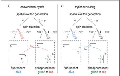
Figure 9: Scheme for the electrical excitation in a) conventional
hybrid and b) triplet harvesting concepts. Here, q denotes the
fraction of excitons that are created on the blue fluorophore, r
STIV
radiative and non-radiative, respectively, and k
F-Pand k
P-Fare
the energy transfers from fluorophore to phosphor or vice versa
(S Reineke, 2013). ... 8
Figure 10 Hopping transport mechanism ... 10
Figure 11 Hopping conduction: a) nearest neighbor hopping
(NNH), b) variable range hopping (VRH).
... 11
Figure 12 Schematic of barrier level for Richardson-Schottky (RS)
thermionic emission: the electric field lowers the surface barrier
by an amount of DΦ, and increases the emission curren.. ... 14
Figure 13 Schematic of barrier level for Fowler-Nordheim
tunnelling
... 15
Figure 14: Plants are able to satisfy their energy requirements by
absorbing light from blue and red part of sunlight spectrum.
. 20
Figure 15 (Symbols) Spectra at different current density for a device
with SimCp as host material (DEV A). (Lines) Spectra at
different current density for a device with CBP as host material.
All spectra are normalized respect to the red peaks at 620 nm.
23
Figure 16: Energy diagrams for DEV A and DEV B. (Red dashed
lines) HOMO and LUMO of red dopant: Ir(btp)2(acac). The red
arrow highlight the reduced step for the electrons to “jump” in
the LUMO level of α-NPD in case of DEV A.
... 24
Figure 17: Current density of DEV C and DEV D. The fast increase
of the current in DEV C is the proof of an easier electron
transport using SimCP instead of CBP at the interface with
α-NPD.
... 25
Figure 18: Energy diagrams for the electron-only devices: DEV C
and DEB D. A deep HOMO level of the BCP near the ITO
avoids the holes injection in the devices.
... 25
Figure 19: At the interface α-NPD÷SimCp electrons jump into
LUMO energy level of the α-NPD. Here, electrons are the
minority charge carriers, so the excitons formation depends on
the electrons recombination.
... 26
Figure 20: (Black Squares) R values for devices with different
V
exponential equation. All the devices were driven at same
current supply of 1 mA.
... 28
Figure 21: (Black Squares) R values for devices with a larger range
of l (2 nm, 4 nm, 8 nm, 35 nm, 60 nm, 100 nm, 150 nm). The
red line points up the behavior of R in a very thin layer of
α-NPD.
... 29
Figure 22: Proposed energy transfer in the purple architecture.
Additional path (k
F-P), to excite the phosphor (Ir(btp)2(acac)
triplet levels, allows to reach an internal quantum efficiency of
100%.
... 30
Figure 23: Number of the red photons (617nm) normalized to blue
photons (453nm). The structure of the devices is: ITO (170
nm)/ PEDOT:PSS (30 nm)/ NPD (60 nm)/ SimCP (d)/
SimCP÷Ir(btp)2(acac) (2%wt) (25nm)/ BCP (9 nm)/ Alq3 (10
nm)/ Ca (20 nm)/ Al (80 nm). The thickness d of the the
intrinsic SimCP tested is: 0 nm, 2 nm, 5 nm, 8 nm.
... 31
Figure 24: Spectra of the purple devices at different thickness of
intrinsic SimCp (above spectra are taken at 5 mA/cm
2as
current supply, the below ones are taken at 10 mA/cm
2).
... 31
Figure 25: Singlet to Singlet Fӧrster transfer is allowed at 0 nm of
SimCp. Introducing an intrinsic layer of SimCp gives an
increment of about 25% of the number of the blue photons, and
it is still high as the intrinsic layer thickness increases,
demonstrating that after 2 nm Fӧrster transfer is negligible..
. 32
Figure 26: A premature triplet-triplet quenching occurs even at low
current density. 2 nm of intrinsic SimCp reduces this effect. A
further increment of the distance between triplet red phosphor
and triplet α-NPD resulting in the extinction of the k
F-Ppath.
32
Figure 27: External quantum efficiency (EQE) of devices under
investigation.
... 34
Figure 28: Purple OLED with active area of ≈ 50cm
2(7cm x 7cm).
Picture was taken at 6 V as voltage supply.
... 35
Figure 29: Picture was taken at 7 V as voltage supply. Here, the
high brightness has saturated the camera, making light as like a
white emission.
... 35
VI
Figure 30: Absolute spectral emission of the purple OLED of 1cm2
at different current supply.
... 36
Figure 31: The CIE (Commission Internationale de l’Éclairge) 1931
coordinates of the device considered in Figure 30.
... 36
Figure 32: a) EL Spectrum of White OLED at different current
supply. b) CIE (Commission Internationale de l’Éclairge) 1931
color space.
... 40
Figure 33: Cross-section of OLED device with metal cathode and
transparent bottom electrode with metal grid.
... 41
Figure 34: Lift-off process used for the preparation of the metal
grids. a) Deposition of the sacrificial photoresist; b) creation of
the inverse pattern on the sacrificial layer (UV
Exposure/Etching); c) metal evaporation; d) washing out the
photoresist together with the metal in excess on its surface; e)
resulting metal pattern.
... 43
Figure 35: Filling Factor (FF) quantifies the area covered by the
metal, namely, it is the relationship between the external area of
the hexagon and the internal one: (Area
1-Area
2)/Area
1.
... 45
Figure 36: (black triangles) Measured sheet resistances for the
metal grids made of Aluminium. (red line) Fitting curve using a
linear fit equation. It is evident how a linear fit doesn’t follow
these data.
... 46
Figure 37: (black squares) Sheet Conductance of the grids as a
function of f
Fof the experimental data. (red lines) Linear fit
according to Eq 28. (green curves) Upper and lower limits of
the 95% confidence interval of the mean value. Values related
to silver grids a), and aluminium b).
... 48
Figure 38: (Red and Black squares) Transmittance plotted vs. the
sheet resistance of the prepared metal grids on ITO. (Black star)
Position on the R
s-T plot of the bare ITO. In the legend: h20
means a metal thickness of 20 nm for the silver grids, and h80
means a thickness of 80 nm for the aluminium grids.
... 50
Figure 39: (Diamonds) Predicted R
s-T position using Eq 29. Except
for the red squares, all values are referred to silver grids. (Black
asterisk) R
s-T position for a silver grid with hexagon side length
VII
of 3 mm, metal width of 150 microns and metal thinness of 20
nm.
... 51
VIII
IX
List of Tables
Table 1 The CIE coordinates are the numerical description of the
chromatic response of an observer to a light source.
... 37
Table 2 Transmittance (550nm) : same values for both kind of
metals
... 45
Table 3 ... 48
Table 4 ... 49
X
XI
Abstract
In this work a potential new OLED application is presented: a large-area purple OLED for horticultural application, which combines red and blue light emissions in a unique device.
The main issue of this thesis is to demonstrate the effectiveness of the proposed OLED structure by using theoretical models created during the three years of the Ph.D. studies and applied to commercial materials.
The core of this dissertation is the third chapter, where the reader is brought to the optimization of the final purple OLED structure after several experiments, which confirm either the basic concepts explained in the two previous chapters, either a mathematical model for a fine-tuning of the blue emission layer.
Behind the proposed device architecture and material employed, there is the concept of “hybrid OLEDs with triplet harvesting”, where a proper combined use of fluorescent and phosphorescent emitting materials allows a theoretical internal quantum efficiency of 100%.
The last chapter is focused on the study and the realization of metal grids on the indium-tin-oxide (ITO), which is the most used material as transparent and conductive anode for the OLED devices.
Despite ITO owns good property of transmittance (transparency), because of its limited conductivity, a lateral voltage drop occurs, preventing a homogeneous emission when the dimensions of the devices exceeds few square centimetres.
To overcome this problem, it is presented a new mathematical model which, unlike the most established literature models do, takes into account both the electrical influence of the metal grid and that one of the ITO.
Finally, with a good agreement with the experimental data, the theoretical model is used to predict optical and electrical behaviour of different hexagonal metal grid on ITO.
It worth to underline that all the approaches implemented in this work to achieve a large-area purple OLED, have a general validity. Indeed, the entire know-how in this thesis it has been successfully used, in the last three years,
XII
to make several different OLED devices, different for colour emission, size and performances.
XIII
Introduction
Organic light emitting diodes (OLEDs) have attracted, in the last thirty years, considerable research interest due to their potential to be used in next generation flat panel displays and low-cost solid state lighting.
The first electroluminescence (EL) in organic materials was observed by Helfrich and Schneider from anthracene in National Research Council, Canada in 1965 (W. Helfrich, 1965)., However no practical application of this technology was seen to be possible due to its extremely high operation voltage (~ 100 V).
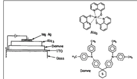
The first work that combined modern thin film deposition techniques with suitable materials and structure, to give a moderately low bias voltage, was made by C.W. Tang and S. VanSlyke at Kodak, who introduced the double layer concept in 1987 (C. W. Tang, 1987). Their devices were made by subliming molecules of a triarylamine as hole transporter, followed by aluminato-tris-8-hydroxyquinolate (Alq3) for electron injection and light generation, and a magnesium-silver alloy cathode (Figure 1).
XIV
The Tang and VanSlyke’s work is a milestone in the organic electronics. The concept of heterostructure has become a standard practice in OLEDs design, and is still adopted nowadays, thirty years later.
Single-layer devices tend to produce unbalanced charge injection and consequently low efficiency of light generation. Instead, using a charge transport or injection layer for holes and one for the electrons, the injected charges from the cathode and the anode are accumulated at the heterojunction, considerably increasing the probability of the electron-hole recombination at this organic/organic interface , which results in the reasonably high efficiency of radiative recombination of this type of devices. Another major breakthrough in OLEDs technology was the fabrication of electrophosphorescent devices, accomplished by Baldo et al. (M. A. Baldo, D. F. O'Brien, Y. You, A. Shoustikov, S. Sibley, M. E. Thompson, and S. R. Forrest, Nature 395, 151 (1998).): these devices significantly increased the internal quantum efficiency as compared to the previous fluorescent devices. Using a phosphorescent dopant in a guest-host system, a nearly 100% internal quantum efficiency can be achieved (see chapter 1).
In terms of applications, the first commercialization of a product based upon the OLEDs was realized by Pioneer® in 1997 - producing the first generation of OLED display. About 10 years later, in 2008, SONY® launched the first commercial OLED TV (11 inches). LG launched the word’s first 55 inches OLED TV at Consumer Electronics Show 2012, setting the future direction of the OLED display market.
Nowadays, the OLED display market is dominated by Samsung and LG. Indeed, OLED technology has recently gained significant market share in the display market. OLED displays are now mass produced for mobile phones, tablets, TVs, and wearables. IDTechEx (www.idtechex.com/) forecasts that market for all types of OLED displays will grow to $57bn in 2026.
The latest evolution is moving towards plastic and flexible displays, compared to conventional glass-based displays: plastic active matrix OLED (AMOLED) panels are much thinner and lighter, enabling either slimmer devices or bigger batteries. Future flexible displays will also make foldable mobile devices a reality. Both Samsung Display and LG Display have recently announced significant investment to expand their production capacity. IDTechEx has upgraded its forecasts and now expects plastic and flexible displays to grow rapidly from a $2bn market this year (2016) to $18bn by 2020.
The rise of plastic and flexible displays will be accompanied by a shift from glass substrates to plastic substrates. However, glass-based displays will remain an important technology, especially in the TV segment where scale-up and cost reduction are still the main challenges.
New applications in wearable devices such as augmented reality (AR) and virtual reality (VR) are also coming to market and provide new
XV
opportunities for suppliers of OLED displays. Sony, Oculus, and HTC have already announced new VR headsets based on AMOLED technologies.
For AR glasses, OLED microdisplays are a major contender against existing LCoS (liquid crystal on silicon) technology.
Figure 2 Plastic and flexible OLED display revenue forecast in four market
segment (Source: IDTechEx)
Beside OLED displays, a very promising field of application is the lighting, in the ever enlarging market of the Solid-State Lighting (SSL) technology, which also include inorganic LEDs and electroluminescent devices.
There are many attractive features of SSL light sources which has placed them as a serious contender in the lighting markets: superior energy efficiency, absence of hazardous metals (mercury free), flexible form factor, high durability and the possibility of intricate light management for energy management and design features. LED-based lighting products have been available for some years now and are the basis for a rapidly growing SSL industry.
OLED technology has been supported through industry-wide projects, especially in Europe, where a large concerted effort has been spent to develop OLED lighting technology. OLED materials and technology development haves been driven by companies and research institutions such as BASF, Merck, Fraunhofer FEP (formerly COMEDD), Novaled, OSRAM, Philips and several universities, to the point where initial OLEDs products for lighting applications are now emerging.
Leading lighting producers such as OSRAM and Philips have introduced limited release commercial products to demonstrate the potential and allow
XVI
interested users to try out OLED lighting technology, with other companies such as Black Body, LG, Pioneer, Konica Minolta, etc. also developing products.
In Japan, advanced prototype OLED lighting products have been shown by a number of local companies, while the US Department of Energy has been instrumental in supporting the technology. Recently, OLED lighting products have even become available through mail-order home supply stores in the USA.
Figure 3 Examples of expected OLED lighting applications(Source: OE-A
Roadmap for Organic and Printed Electronics)
OLED lighting products promise novel features in the longer term: large emitting area, diffuse light emission without glare, flexibility and very thin form factors, high efficacy, variable color, and even transparency are just some of the possibilities. New lighting applications can be expected to take advantage of the OLED properties, for example embedded lighting or homogeneous area lighting.
The lighting market is however complex, as it is a highly fragmented space thanks to the existence of a broad technology mix and a diversity of customer needs. The market segments include residential, office, industrial, outdoor, hospitality, museums, shops, automotive, agriculture, and more. Each sector attaches a different degree of importance to upfront cost, energy efficiency, lifetime, light intensity, color warmth and design features. This explains why the technology mix in each sector is different.
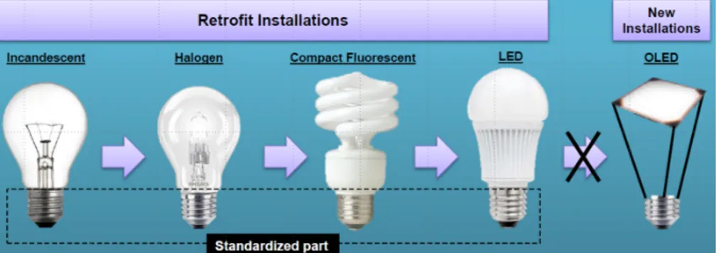
IDTecEx assess that the OLED lighting market will grow to 2.2 billion USD in 2026 (optimistic scenario). The market growth will however be very slow until 2019/2020, where the overall sales at panel level will remain below 200 million USD globally. Furthermore, to effectively exploit the properties of the OLED sources, new installations will be necessary, instead to use them as retrofits in existing installations ( Figure 4).
XVII
Figure 4 A new OLED module could not fit any existing lamp, particularly
for that based on the classic light bulb
OLED lighting has the potential to efficiently emit warm light across large surfaces and to bring new and novel form factors into the lighting sector. These are strong selling points on their own, but the challenge is in that they are not always unique. In particular, inorganic LED lighting arrived first onto the market. Its technology, cost structure and supply base have dramatically improved, opening a large performance and cost gap between LEDs and the younger OLEDs. The performance gap has not drastically narrowed despite progress in OLEDs, with companies such as Konica Minolta reporting champion 131 lm/W panels.
The challenge OLEDs are facing is therefore identifying paths for differentiation. The differentiation challenge is also a critical strategy question, because many companies, such as OSRAM and Phillips already have successful and growing businesses in the LED sector.
Surface emission is a possible differentiator, although inorganic LEDs are also able to create effective surface emissions thanks to waveguides, despite they are point light sources. Flexibility is also another way, although OLEDs themselves also face critical technology challenges that stand in the way of them achieving flexibility.
The ability to offer customized or improved design features is also a selling point. In particular, the potential to act at the luminaire level as a slightly modified panel can be a competitive advantage (Figure 5).
XVIII
Figure 5 A recent example of an OLED luminaries installation
From a technological point of view, there are two main approaches to fabricate OLEDs: vacuum deposited small molecule OLEDs and solution processed polymer OLEDs. The former type has been more efficient and therefore the leading technology for lighting. OLED products are currently restricted to rigid glass substrates.
Flexible OLEDs are possible on plastic and metal foils. Furthermore, flexible ultrathin glass appears on the horizon as an attractive substrate. In time, hybrid materials and manufacturing approaches may be used to realize actual OLED lighting products, in order to optimize manufacturing economics.
Current lighting sources present a broad range of competing performance capabilities, and lighting applications are very varied. Competing against existing products will not be made any easier by the prospect that in the short term OLEDs will tend to be non-transparent, small area and on rigid glass substrates. However, already now, OLED benefits can be envisaged, whether due to the novel surface emission for design applications or by virtue of the thinness where space is at a premium.
A number of key parameters for OLED lighting are generally discussed in the industry. The three critical parameters are lifetime, luminance and efficacy. Other important parameters include size, cost and the light quality parameters color rendering index (CRI) and color temperature.
At industry level, parameter definition and reporting standards must be developed, to assure end- users in the lighting industry.
• Lifetime: this refers to T80 (time to 80% initial luminance). A minimum lifetime of 10,000 hours is necessary to support initial applications
XIX
in illumination. In the longer term, given the expectations set by LED lighting, 50,000 to 100,000 hours will be required.
• Efficiency: the conversion from electrical energy to light is a critical measure for lighting. 50 lm/W and higher is now available to be competitive and meet new efficient lighting regulations. Lower luminaire losses are to be expected for OLEDs than for other forms of lighting, due to the unique surface emission properties.
• Size: as an area light source, OLED success depends on scalability to large area. Form factors in the range from 10 cm2 and up to 60 cm 2, either
using single devices or arrays of devices, are suitable for lighting products. • Luminance: area light emitters for ambient or signage lighting are referenced in terms of brightness per unit area (cd/m2). Low levels in the
region of 100- 300 cd/m2 may be sufficient for automotive interiors. High
unit lumen output for general lighting will require up to 5,000 cd/m2, but this
will need to be balanced against lifetime.
• Cost: two basic valuations may be considered for OLEDs. For general lighting, OLED light cost needs to be less than 1 euro cent per lumen for mainstream acceptance. However, cost per unit area (for ambient or backlighting) should be in the region of 500-1000 €/m 2.
Core OLED lighting technology has borrowed heavily from OLED display development. There are a number of critical issues related to commercialization: on the one hand, developing components and technologies for outcoupling and encapsulation that are both higher performing and suitable for mass manufacturing is essential for commercial product development. On the other hand, the development of highly efficient and scalable manufacturing processes for reliable and cost effective OLED devices is a must: solutions are in sight, but progress cannot to be taken for granted.
• Encapsulation: the high sensitivity to moisture of OLED materials makes the integrity of current encapsulation methods (glass cap, getter) critical to ensure lifetime performance in the short term. Thin film encapsulation could enable large area, flexibility and integrated in- line production. There are indications that this issue can be tackled in the near future. In order to reduce devices cost and accelerate commercial uptake, the development of new barriers (e.g., inorganic/organic multilayer, laminates) is needed.
• Outcoupling: OLED efficiency can be improved considerably by the use of suitable light extraction and light management techniques, in the form of optical components and structures. Integration into the OLED structure, e.g. in the form of intelligent glass substrates or lenses (microlenses array, pyramids array, prisms foil), index-matched materials and adhesives, that can be introduced into high volume manufacturing processes, is an important area needing further development. Good encapsulation would allow for use
XX
of plastic substrates with better opportunities to achieve improved outcoupling.
• Standardization: Reporting standards need to be established and adhered to (lifetime, structure, improvement factors).
• Manufacturing costs: in view of the current high price of OLED manufacturing and the needed low cost for general lighting, improved manufacturing processes, that enable lower price points and potential for much higher volumes for lighting products, are required. Higher throughput and material utilization efficiency are required from vacuum deposition equipment. Solution processing and printing tooling promises lower cost manufacturing, but needs to be capable of delivering high performance devices. This is becoming the most dominant challenge.
• Investment: moving from R&D and pilot lines to real production is strongly needed to enable broad applications for the OLED lighting technology, but it requires large investments.
In this context lies this thesis.
A particular sector of the lighting is receiving large attention in the last years, the horticultural lighting. In this regard, it is noticeable that in 2016 the Horticultural Lighting Conference was started (http://www.lighting-inspiration.com/event/horticultural-lighting-conference-2016/).
Large area OLED for horticultural application could offer great advantage to the emerging market of LED for horticultural, strongly pushed by OSRAM and Philips (see chapter 3).
1.Organic LEDs
1.1. Functional layers
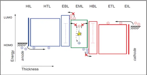
In principle, an organic light emitting diode consists of a sequence of organic layers between two electrodes, an anode for holes and a cathode for electrons injection, respectively (Figure 6).
Under positive bias, holes are injected from the anode and electrons from the cathode. The charge carriers drift through the layers and meet in the emission layer (EML). Here, they form excitons (neutral excited states) which show a certain probability to decay radiatively (S. Reineke, 2012), allowing the photon emission: this phenomenon is called Electroluminescence (EL).
To achieve highly efficient OLEDs, they have become complex multilayer systems, where each layer has different and specific functionality. Figure 6 illustrates a multilayer OLED sequence with its functional layers. For simplicity, in Figure 6, the highest occupied molecular orbital (HOMO) and lowest unoccupied molecular orbital (LUMO) levels are treated similar to valence and conduction bands in inorganic semiconductors. and the vacuum level is assumed to be aligned. It is worth keep in mind that this is a very rough approximation.
Chapter 1
2
Figure 6: (color online) Energy diagram of a typical multilayer OLED.
Note that in many devices some of the layers depicted are redundant, because different functions may be combined in one layer. From anode to cathode there are: hole injection layer (HIL), hole transport layer (HTL), electron blocking layer (EBL), emission layer (EML), hole blocking layer (HBL), electron transport layer (ETL), and electron injection layer (EIL). Boxes indicate HOMO and LUMO levels of the materials. The dashed lines in the EBL, EML, and HBL are the desired triplet energies of the materials in case of phosphorescent OLEDs. (S Reineke, 2013).
Holes are injected from a high work function material (the most used, in case of bottom emission OLEDs, is the transparent conductor indium tin oxide (ITO)) into the HOMO level of an organic semiconductor: the hole transport layer (HTL). For an improved injection, a thin hole injection layer (HIL) is used to ease hole injection from the anode into the hole transport layer. This can be achieved by choosing its HOMO level in between the HOMO of the HTL and the ionization potential of the anode Figure 6. A good way to achieve a high performing OLED is to sandwich the EML between the EBL and the hole blocking layer (HBL), in order to confine both the types of carriers as well. The double confinement of the EML keeps spatially separated the excitons from the HTL and ETL, because these layers might be luminescence quenchers or, in case of HTL /ETL materials with a high photoluminescence quantum yield (PLQY), they could act as undesired emission layers, altering the expected device color emission and affecting the whole device efficiency.
Organic LEDs
3
1.2. Fluorescent and phosphorescent materials
As mentioned, charges are injected in the EML under the influence of an electric field. At separation of a few nanometers, the Coulombic attraction binds the charges together and they are no longer able to escape one another by thermal diffusion. As a consequence, the total spin of the hole-electron pair can be either S=0 or S=1.
The S=0 is due by the antisymmetric spin interaction of the hole-electron pair and is known as singlet state; instead, the S=1 contains three possible states, all symmetric, and is known as triplet state.
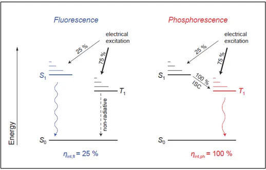
Because the triplet state has a multiplicity of three, on average 75% of the excitons formed are triplet states, with the remaining 25% being singlets.
The spin of the exciton controls its luminescence. Because the emission of a photon conserves spin, quantum-mechanically, only singlet excitons are allowed to decay radiatively. This process is fast (particle lifetimes of ≈ 1 ns), and is known as fluorescence. In contrast, the probability of luminescence from the remaining triplet states is generally so low that almost all their energy is lost to non-radiative processes, with particle lifetimes in the order of 1 ms. This emission from a “disallowed” transition is known as phosphorescence.
The low singlet fraction causes OLEDs based on fluorescent emitter molecules to be rather inefficient, with an upper limit of the internal quantum efficiency of ηint,fl = 25%, because emission solely occurs in its
singlet manifold as shown in Figure 7.
The efficiency of OLEDs can be drastically improved with the introduction of phosphorescent emitting molecules (M.A.Baldo, 1998), (S. Reineke, 2012). It is well known that heavy metal atoms, such as iridium, platinum, palladium, etc., can enhance spin-orbit coupling within a molecule or polymer, weakening the selection rules for previously forbidden transitions (Thompson, 2007), (H. Yersin, 2002), (Yersin, 2004). In these materials, called organometallic complexes, the emission of light is still significantly slower than fluorescence, but the radiative decay rate is faster than the non-radiative one, then the luminescence can be efficient. Simultaneously, the introduction of the heavy metal strongly enhances the intersystem crossing (ISC) rate between singlet and triplet state, with a very high efficiency, close to unity. So, the 25% of singlet excitons are efficiently converted into triplet state, before they can recombine radiatively. Therefore, a phosphorescent OLED material can lead to ηint,ph = 100%.
Chapter 1
4
Figure 7: Population scheme of singlet and triplet level of the organic
molecules under electrical excitation. For phosphorescent materials, the singlet excitons created are efficiently transferred to the triplet state via intersystemcrossing (ISC). Additionally, the theoretical limits for the internal quantum efficiency ηint are given.
1.3. Host-guest system
Phosphorescent materials exhibit at least one order of magnitude longer excited state lifetime compared to conventional fluorescence dyes. Then, these excitons are highly exposed to non-radiative “quenching” processes, that limit the device efficiency at high excitation levels, the “efficiency roll-off”. A high exciton density increases the probability of the excited state annihilation process, such as triplet-triplet annihilation, triplet-polaron quenching (M. A. Baldo, 2000), (S. Reineke, 2007), and in some case field-induced exciton dissociation. In order to reduce these quenching effects, the phosphorescent material is dispersed into another material (host-material). High quantum yields are typically achieved with a concentration of the phosphor (guest-material) in the host-guest system in the range of 1-10wt%.
In a host-guest system, excitons formed in the host are transferred to the luminescent dye via a combination of Fӧrster and Dexter energy transfer (M. Klessinger, 1995).
Organic LEDs
5
Figure 8 Proposed energy transfer mechanisms in films doped with a
fluorescent dye (a and b), and films doped with a phosphorescent dye. For each molecule, it is shown the ground-state energy level S0, the excited-state singlet level S1 and the excited-state triplet level T1
Fӧrster transfer is a long range ( ~40 – 100 Å), dipole-dipole coupling of donor (D) and acceptor (A) molecules. Since it requires that the transitions from the ground to the excited states be allowed for both D and A species, this mechanism only transfers energy to the singlet state of the acceptor molecule (T. Fӧrster, 1948).
Dexter transfer, instead, is a short range process where excitons diffuse from D to A via intermolecular electron exchange, which required orbital overlap of D and A, resulting in a decrease of this interaction with increasing intermolecular distance (Dexter, 1953). Dexter processes require only that the total spin of the D-A pair be conserved under the Wigner-Witmer selection rules (M. Klessinger, 1995). Consequently, Dexter transfer permits both singlet-to-singlet and triplet-to-triplet transfers.
For a full understanding of all the energy transfers involved in a host-guest system, (M.A. Baldo, 1999) summarizes the energy pathways that could be responsible for the photons emission in a phosphorescent guest and a fluorescent one.
In case of a fluorescent dye, it is shown the singlet-to-singlet transfer Figure 9a), ): although both Fӧrster and Dexter processes are capable of singlet-to-singlet energy transfer, Fӧrster mechanism dominates (V. Bulovic, 1998) at low fluorescent dye concentrations because of its long-range nature.
Chapter 1
6
On the other hand, a guest triplet state could be excited at close range by triplet-to-triplet Dexter transfer Figure 9b) Unfortunately, most fluorescent dyes have very short radiative lifetime (~ 10 ns), so at room temperature, phosphorescence is rarely observed and non-radiative losses are dominant. Therefore, the process in Figure 9a) can be considered the responsible for the luminescence in the most fluorescent organic dyes spread in a host material.. Figure 9c) shows singlet-to-triplet transfer between a host and a phosphor: here it is expected that Fӧrster singlet-to-singlet transfer is still the dominant process. Then, thanks to the ISC, with near the unity efficiency, all the singlet excitons are transferred to the triplet ones inside the guest material. Finally, Figure 9d) represents direct Dexter transfer between triplet states of the host and triplet ones of the phosphor dopant.
Let’s note that, the host material must be selected carefully with respect to the guest’s energy levels. Once the exciton is transferred to the guest sites, it is necessary to confine the exciton on the phosphor so that radiative recombination can occur efficiently (S. Su, 2008), (K. Goushi, 2004). Therefore, the relative position of the host triplet level Thost respect to the
phosphor triplet state Tguest is important. The highest phosphorescence
quantum yield of the host-guest system can be expected only for exothermic system, where the triplet level of the host is higher in energy compared to the phosphor (Thost > Tguest). By reducing the energy of the host triplet to a
resonant or endothermic system and, hence, allowing back transfer from
Tguest to Thost, the phosphorescent quantum yield of the host-guest system will
decrease accordingly, as more excitons remain on the host sites (S.Reineke, 2009).
Finally, another parameter that plays a key role in the working principle of OLEDs is the exciton diffusion. Under electrical excitation, excitons are formed close to an interface between different materials, usually with a generation width below 5 nm (S. Reineke, 2007), thus smaller compared to the total layer thickness (S. Reineke, 2007), (Y.R. Sun, 2006), (J. Wünsche, 2010). Both Fӧrster and Dexter energy transfers do not forbid excitons to migrate throughout organic solids. Here, the net charge carrier is zero, so the only driving force is a gradient in the exciton concentration, leading to a series of uncorrelated hopping steps from molecule to molecule (S Reineke, 2013).
1.4. Hybrid OLEDs and Triplet harvesting
The combination of a fluorescent blue emitter with phosphorescent dyes to form hybrid multicolor OLEDs ( i.e. white OLED) is attracting much interest, because it could provide an alternative to use of blue phosphors, which are the current bottleneck in the development of a very efficient white devices.
Organic LEDs
7
The reason of these relevant drawbacks are: i) hardly the emission from blue phosphor extends till deep blue region of the visible spectrum, common photoluminescence peak is around 460-470 nm (A. Endo, 2008); ii) blue phosphorescent materials with long term of stability are hard to find (S.Reineke, 2009), (S. Su, 2008); iii) because blue phosphorescent materials need of host materials with even larger bandgap, the operating voltage of devices based on phosphorescent blue emitters will increase (Y. Kawamura, 2005), (N.Seidler, 2010).
In the conventional hybrid architectures, the blue fluorescent emitters used have triplet level T1 lower than the respective triplet states of the
phosphorescent materials. In Figure 9a), it is depicted a possible scheme for the excitation in a conventional hybrid architecture. Here, excitons are created with a fraction q on the fluorescent emitter, leaving 1-q to be generated in the phosphorescent system (green to red). All formed excitons obey the spin statistics presented in the previous section, where the fraction of created singlets is indicated with rST. Note that in general, rST may be
different for every emitter system (M. Segal, 2003). However, to keep this discussion simple, for rST it is used the same value for any emitter system
here.
Since the triplet level of the fluorescent blue emitter is lower than the respective levels of the phosphorescent materials, efficient transfer from T1
of the phosphors to that of the blue fluorescent dye can occur, represented by the rate kP-F. The latter triplet level is non-radiative (nr), thus excitons
reaching it will be lost for emission, forming a quenching channel for triplet excitons. A way to extinguish this channel is to introduce a thin interlayer between fluorescent and phosphorescent system. The energy transfer leading to a kP-F > 0 is Dexter type, requiring orbital overlap, so an interlayer
thickness of 2 nm is sufficient (S Reineke, 2013).
In this architecture, another non negligible exciton quenching channel is due to the direct formation of triplet excitons on the fluorescent triplet level, which is proportional to q*(1 - rST). According the theory explained in the
section 1.2, (1 - rST) is in the order of 75% (triplet states formation rate), the
only way to reduce this channel is to reduce q. However, this will decrease the fluorescent intensity at the same time (q*rST).
Chapter 1
8
Figure 9: Scheme for the electrical excitation in a) conventional hybrid
and b) triplet harvesting concepts. Here, q denotes the fraction of excitons that are created on the blue fluorophore, rST is the fraction of singlet
excitons formed, `r' and `nr' stand for radiative and non-radiative, respectively, and kF-P and kP-F are the energy transfers from fluorophore to
phosphor or vice versa (S Reineke, 2013).
The only way to reduce the losses leading to the two above explained quenching channel is to use a fluorescent blue material with a T1 level
higher, or at least equal, than the T1 level of the phosphorescent emitters
(Figure 9b). The different relation of the energy levels reverse the direction of the energy transfer, transforming the quenching rate kP-F into an additional
path (kF-P) to excite the phosphor triplet levels. If this triplet harvesting
mechanism is incorporated inside the device, it allows to reach an internal quantum efficiency of 100%.
The triplet harvesting concept is based on the fact that non-radiative triplets formed in the fluorescent materials can find accessible sites for recombination which are spatially separated and only reached via diffusion. The consequence of the triplet diffusion into the emissive phosphorescent sites is a higher likelihood of the triplet-triplet annihilation, so that the quantum efficiency of the green to red system is strongly reduced as a function of the exciton level, thus current level (roll-off). So, it must be kept in mind that the exciton generation zone it should be such that the average distance a triplet has to travel to reach a phosphor site is as short as possible.
2.Electrical behavior and
modeling
2.1. Introduction
So far, it was explained the mechanisms behind of OLEDs operation, from the excitons formation to photons emission. Before forming the excitons, two fundamental steps happen: carriers injection from the metal contacts, and carrier transport in the bulk material. These two processes have impact on the electrical behaviour of an OLED.
The purpose of this chapter is to provide a brief presentation of the scenario regarding transport mechanisms in materials used in the OLED devices. This topic is large and not trivial; for a more complete treatment of this subject, the reader should refer to the specialized papers indicated in the text.
To describe most of the physical mechanism in an organic material is common to use many concepts derived from inorganic semiconductor physics, as it was done for the following physical models shown in this chapter. However, there are some peculiarities and differences of organic semiconductor to their inorganic counterpart.
Since most polymeric and small molecules based materials for OLEDs form disordered amorphous films without a macroscopic crystal lattice, it is not possible to adopt mechanisms developed for molecular crystals.
Because of the absence of extended delocalized states, charge transport is usually not a coherent motion in a well defined bands, but rather a stochastic process of hopping between localized states, which leads to the typically observed low carrier mobility (µ << 1 cm2/V s).
Additionally, many of the materials in OLEDs are wide-gap materials with energy gaps of 2-3 eV, or even more. Therefore, the intrinsic concentration of thermally generated free carrier is generally negligible (<
Chapter 2
10
1010 cm-3) and from this point of view these materials can be considered more as insulators than as semiconductors (W. Brütting, 2001).
As explained in the previous chapter, in an OLED there is the necessity to use contacts with different work function (usually high work function as anode, and low work function as cathode) in order to obtain double-carriers injection at the base of the exciton formation. Using contacts with different work function leads to the presence of non-negligible built-in voltage Vbi
across the organic layers.
Neglecting the energy level shift due to the interface dipoles, the built-in voltage is equal to the contact-potential difference of the two electrodes. So, the physical importance of Vbi is that it reduces the applied external voltage
V, such that a net drift current in forward is achieved if V exceeds Vbi. Thus,
in the following equations, there will be the tacit assumption that the affective voltage across the organic layers under forward bias condition is V = VForward - Vbi.
2.2. Charge transport in organic material
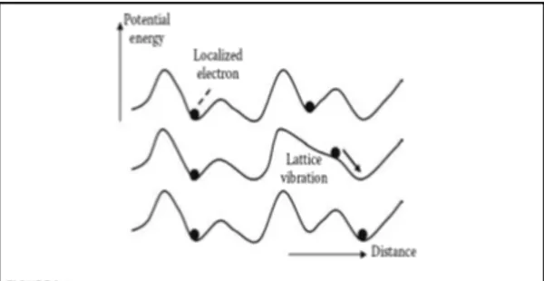
Only in the very special case of high material purity, low temperature and high crystallinity, organic materials can exhibit band-like transport behavior similar to that one of classic inorganic semiconductor. More often, organic semiconductors show a disordered structure, so the charge carriers move inside them through an intermolecular process of hopping between adjacent molecules.
Furthermore, charge carriers can be localized by defects, disorder or potential wells caused by the polarization. If the lattice is irregular or the carrier becomes localized on a defect site, the lattice vibrations are essential to let the carrier move from one site to another. This is an activated process and the mobility increases with increasing temperature.
Electrical behavior and modeling
11
Independently from the specific mechanism of the charge movement, conduction based on electron movement can be described by the relation 𝐽 = −𝑞𝑛!𝜇!𝐸, where J is the current density, q is the elementary charge, ne
electron density, µe electron mobility and is defined as: 𝜇! =!!!, and vd is the
drift velocity of the electrons.
The mechanism of the electron movement is hidden within the electron mobility µe that represents the relation (ratio) between applied field strength
and drift velocity.
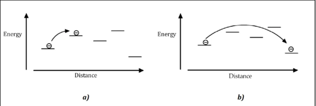
Focusing on the most common case of disordered organic materials, two models are here illustrated, applied to describe the hopping conduction mechanism: the Nearest Neighbor Hopping (NNH) and the Variable Range Hopping (VRH). In the former, an electric charge “jumps” from a spatial localized energy level to the nearest neighbor (Figure 11a), while in the latter the charge can jump several levels away from the original one, i.e. variable range (Figure 11b).
Figure 11 Hopping conduction: a) nearest neighbor hopping (NNH), b)
variable range hopping (VRH).
The transition probability from one energy level to another is expressed as the product of some terms, taking into account:
• wavefunctions overlapping between states: this term has an exp(-αR) dependence, where α-1 is the wave function localization length
and R is the distance between initial and final levels;
• Phonons availability: if the initial and final states have energy separation of E, energy conservation rules require a second particle bridging this gap, in order to enable the charge hop. This mechanism is generally fulfilled through molecules vibration, i.e.
Chapter 2
12
phonons. The term dependence is exp(-E/kBT), where kB is
Boltzmann constant and T is temperature;
The probability (p) per unit time of a charge jumping between two localized states is therefore proportional to:
Eq 1
exp(-Q)
~
p
; Eq 2⎟⎟
⎠
⎞
⎜⎜
⎝
⎛
+
=
T
k
BE
R
Q
α
;When E is smaller than kBT, the αR term dominates, leading to a NNH
mechanism; Q is minimized for minimum R, when the final level is the nearest one. On the other hand, when T is low and phonons energy and number are small; E/kBT cannot be neglected with respect to αR. In this
situation, balancing energy and distance, a distant level could possess a smaller Q than the nearest neighbour and a VRH regime occurs.
Hypothesizing a casual diffusive mechanism as the driving force of the electron motion, electrical conductivity σ in hopping regime can be calculated as follow: Eq 3
µ
σ
=
qn
; Eq 4 T kB qD =µ
; Eq 5 26
1
pR
D =
;Here, q is the electron charge, n is the electron density and µ is the charge mobility, determined by the Einstein relation. D is the diffusion coefficient, in which hopping probability is taken into account according to NNH
Electrical behavior and modeling
13
mechanism. On the contrary, in the case of VRH regime, conductivity has the characteristic temperature dependence expression
Eq 6 4 1 0 0
exp
⎟
⎠
⎞
⎜
⎝
⎛
−
=
T
T
σ
σ
;where T0 and σ0 are constant given by model parameters (R, α, etc.).
2.3. Charge carrier injection and transport in OLED
There are two limiting regimes of device operation for an OLED, namely space-charge limited current (SCLC) and injection limited current.
• Injection limitation occurs if the injection barrier is so large that injection from the contacts does not provide an inexhaustible carrier reservoir.
Carrier injection into semiconductor is usually treated by Richardson-Schottky (RS) thermionic emission (S.M.Sze, 1981), based on lowering of the image charge potential by the external field F = V/d. The current density JRS as a function of the field is given
by: Eq 7
with the Richardson constant A* = 4πqm*k
B2/h3 (= 120 A/cm2K2)
for m* = m
0), βRS = √(q3/4πεε0), ΦB is the zero-field injection barrier.
(q: elementary charge; m0: free electron mass; kB: Bolzman’s
constant; h: Planck’s constant; ε relative dielectric constant, ε0:
vacuum permittivity).
J
RS(F) = A
*T
2exp(−
Φ
B−
β
RSF
K
BT
)
Chapter 2
14
Figure 12 Schematic of barrier level for Richardson-Schottky (RS)
thermionic emission: the electric field lowers the surface barrier by an amount of DΦ, and increases the emission curren..
Another injection mechanism is the Fowler-Nordheim (FN) tunnelling (Figure 13), where unlike RS emission, Coulombic effect of the image charge is ignored and it is considered only the tunnelling through a triangular barrier into continuum states:
Eq 8 with
J
FN=
A
*q
2F
2Φ
Bχ
2k
B2exp(−
2χΦ
B 2 33qF
),
χ =
4π 2m
*h
Electrical behavior and modeling
15
Figure 13 Schematic of barrier level for Fowler-Nordheim tunnelling
• SCLC in an OLED can occur if at least one contact is able to inject locally higher carrier densities than the material has in thermal equilibrium without carrier injection. This problem was extensively treated by Lampert and Mark, studying SCLC in insulators (M.A. Lampert, 1970). In case of a perfect insulator, without intrinsic carriers and traps and for a charge carrier mobility independent of the electric field, the SCLC obeys the Mott-Gurney equation (N. F. Mott, 1940):
Eq 9
. where d is the device thickness.
In the presence of traps, if they are distributed in energy, they will be gradually filled with increasing electric field, then, the current will increase faster than quadratic until all traps are filled (W. Brütting, 2001).
A fully analytic derivation, in case of trap-charge limited current (TCLC), considering the following trap exponential energy distribution, Nt is the total
trap density and a characteristic decay energy ET:
Eq 10 is given by: JSCLC= 9 8