Abstract
In the modern society, the reduction of the energy consumption through its efficient use has become one of the main task of power electronics. In this context, Silicon Carbide (SiC) exhibits interesting electrical and physical properties which can satisfy the continuous demands of improved energy efficiency, overcoming the limitations of Silicon. Today several SiC technologies have reached the industrial maturity. In this thesis, different aspects and challenges related to the fabrication of 4H-SiC MOSFETs (which are among the most appealing devices due to their driving simplicity) have been treated. Indeed, in spite of remarkable and recent progress, several scientific aspects still need to be dealt for reducing the energy dissipation and to overcome the issues still open. In particular, the aim of this thesis has been to clarify the mechanisms ruling the transport properties at the interfaces metal/SiC and SiO2/SiC. Special focus was given to the study of the mechanisms limiting the channel mobility in lateral MOSFET. All the achievements and progresses obtained have been integrated in a power MOSFET device, whose behaviour has corroborated the great potential of the material.
Riassunto
Nella società moderna la riduzione del consumo di energia attraverso un suo uso efficiente è diventato il compito principale della elettronica di potenza. In questo contesto, il carburo di silicio (SiC) presenta interessanti proprietà fisiche ed elettriche che permettono di soddisfare le continue esigenze di miglioramento dell'efficienza energetica e di superare i limiti del silicio. Oggi diverse tecnologie in SiC hanno raggiunto una maturità industriale. In questa tesi sono stati affrontati diversi aspetti e problemi relativi alla fabbricazione di dispositivi MOSFET in 4H-SiC (che sono tra i dispositivi più interessanti a causa della loro semplicità di pilotaggio). Infatti, nonostante i notevoli recenti progressi, ancora numerose sfide scientifiche devono essere affrontate per ridurre la dissipazione di energia e superare le questioni ancora aperte. In particolare, lo scopo di questa tesi è stato quello di chiarire i meccanismi che regolano le proprietà di trasporto alle interfacce metallo/SiC e SiO2/SiC. Un’attenzione particolare è stata dedicata allo studio dei meccanismi che limitano la mobilità di canale nei MOSFET laterali. Tutti i risultati e i progressi ottenuti sono stati integrati in un dispositivo MOSFET di potenza il cui comportamento ha confermato il grande potenziale del materiale.
i
The science of today is the technology of tomorrow
ii
Contents
Acknowledgments
...vIntroduction
...1Chapter 1
: Properties of SiC...91.1 Structural properties and polytypes of SiC......9
1.2 Electronic properties of SiC...13
1.3 References...21
Chapter 2
: Planar Power MOSFET for energy efficiency...232.1 Power applications and advantages of Silicon Carbide...24
2.2 Power MOSFET in SiC and figures of merit...26
2.2.1 MOSFET: basic operation principles and output characteristics...33
2.2.2 Contributions to the Ron in a planar MOSFET...34
2.3 Technology issues for 4H-SiC MOSFET fabrication...39
2.4 References...41
Chapter 3
:
Ohmic contacts on p-type SiC...433.1 Ohmic contacts for SiC devices...43
3.2 Specific contact resistance in metal/semiconductor Ohmic contacts...47
3.3 Experimental details...51
3.4 Surface morphology of implanted 4H-SiC and Ti/Al Ohmic contacts...54
3.5 Specific contact resistance of Ti/Al Ohmic contacts...56
3.6 Temperature dependence of the electrical properties of implanted 4H-SiC and Ti/Al Ohmic contacts...58
Contents
iii
3.8 Ohmic contacts for MOSFETs devices...68
3.9 Conclusion...69
3.10 References...71
Chapter 4
:
Channel mobility in 4H-SiC MOSFET...754.1 Channel mobility: a critical issue for 4H-SiC MOSFETs...75
4.2 Lateral MOSFET: mobility and threshold voltage...77
4.3 Fabrication of 4H-SiC lateral MOSFETs...84
4.4 Electrical characterization of the lateral MOSFET...89
4.5 Temperature dependence of the channel mobility...91
4.6 Temperature dependence and instability of threshold voltage...97
4.7 A different approach to increase the mobility: POCl3 annealing...99
4.8 Conclusion...104
4.9 References...105
Chapter 5 :
4H-SiC vertical power MOSFET...1095.1 Background...109
5.2 STM MOSFETs...112
5.3 Electrical Characteristics of STM 4H-SiC MOSFET...113
5.3.1 Static Behaviour...113 5.3.2 Dynamic Behaviour...117 5.4 Conclusion...121 5.5 References...122
Conclusion
...123Publications
...127Contents
v
Acknowledgements
It is anything but easy thank all the people who contributed to my personal and professional development during my Ph.D. studies.First of all, I extend my deepest thanks to Dr. Fabrizio Roccaforte for his guidance and for his scientific suggestions during my doctoral study. I will ever be grateful to him to have me allowed to achieve important goal. I also owe Dr. Mario Saggio many thanks for his great assistance and encouragements during the PhD years and the ST work.
More than anyone else, I want to thank Dr. Vito Raineri, unfortunately no longer with us, for the opportunity he gave me to work on various challenging and interesting areas.
I should never finished this work without the precious help and daily support of Dr. Alfio Guarnera from ST: endless thanks.
Big thanks go out also to Prof. Mario Cacciato from the University of Catania, tutor of the thesis for his comprehension whenever I requested something from him.
Of course, another profound thanks is for all people of the CNR-IMM, who have contributed to this work of thesis. In particular, I thank: Dr. Filippo Giannazzo for his precious discussions and valuable contributions in the AFM analysis; Dr. Raffaella Lo Nigro for her exquisite scientific discussions and the interpretation of XRD analysis; Dr. Patrick Fiorenza for his encourages during the CNR-IMM years. I want also to thank Salvo Di Franco for his valuable support during the devices processing in the CNR-IMM clean room. Finally, special thanks to Corrado Bongiorno and Salvo Pannitteri for the useful TEM analysis and discussions.
I am indebted to my colleagues at STMicroelectronics for providing a stimulating environment in which to learn and grow. I especially grateful to Simone Rascunà, Edoardo Zanetti, Dario Salinas and Leonardo Fragapane. Every one of them have had an important role in this adventure.
Thank you to all friends, who accompanied me in this experience and shared with me the “box 2” during the CNR-IMM years: Giuseppe Greco, Carmelo Vecchio, Jens Eriksson and Sushant Sonde.
Acknowledgment
vi
I would like also to thank all the people who assisted and believed me in this years. A special acknowledgment is due to my parents Lino e Cetty who always encouraged me in my studies and learned to live. A particular acknowledgment is due to my sisters, Simona and Ilaria, and my brother, Fausto to make special every instant of my life. Finally, a lovely acknowledgment is dedicated to my husband Andrea, who made this thesis possible by his support and unrivalled Love.
Thank you everyone Alessia
1
Introduction
We live in an energy-hungry world in which industrialization and globalization have accelerated the demand for resources that now doubles approximately every 40 years. Microelectronics research activity has grown with a nearly exponential rate. In parallel to the advent of the continuous progresses leading to the miniaturizing of the devices and integrated circuits, the reduction of the energy consumption through its efficient use is the main task of modern power electronics. The increasing dependence of power electronics in modern society has motivated great advances in power electronics technology. These advances are significantly dependent on performance enhancements of power devices that have been widely used in power generation and power distribution. Three driving forces make reducing energy losses a major priority. The first is the Kyoto Protocol that sets binding obligations on industrialized countries to reduce emissions of greenhouse gases. The second is the rising cost of energy, which incites everyone to cut down on its use. The third driving force is the fact that the majority of the world’s energy comes from hydro-carbons and only 15% from renewable energy.In the last six decades Silicon (Si) technology has always dominated the power electronic field, providing semiconductor devices able to operate in a broad spectrum of power levels and frequencies. Due to the inherent limitations of Silicon material properties, such as narrow bandgap, low thermal conductivity and low critical electric field, Silicon power devices are approaching theoretical limits in terms of higher power and higher temperature operations, offering no significant improvement in device performances with further investment.
Hence this material is no longer suitable for modern power electronics application [1,2]. The demand for improved energy efficiency in power electronics, which can be satisfied by reducing the switching and conduction losses of devices, as well as for devices capable of high temperature operation, is pushing the power electronics technology development toward wide band gap (WBG) semiconductors. In this context, Silicon carbide (SiC), gallium nitride (GaN), exhibit interesting electrical and physical properties that can satisfy the continuous demands of improved energy efficiency. SiC has been recognized, among all the WBG materials, as a good candidate for replacing
Introduction
2
silicon [3] in certain power device applications [4]. First of all, SiC has a great advantage over competing compound semiconductors in the fact that, like silicon, it has silicon dioxide (SiO2) as its native oxide. Moreover, thanks to the commercial
availability of large size SiC wafers accompanied by an improvement in the quality of substrates (micropipes reduction) [5] and to the achievement of a high level of maturity in manufacturing processes, several SiC technologies, operating at different voltages (600V and 1200V), have reached the industrial maturity [6,7,8,9]. SiC switches available in the market are junction field effect transistors (JFETs), barrier junction transistors (BJTs) and metal-oxide-semiconductor field effect transistors (MOSFETs). The MOSFET is the most promising technology, due to its driving simplicity and market appeal.
SiC-based electronic devices can work at higher temperature, higher power and higher frequency and in environments harsher than the current traditional semiconductor technology may afford. Therefore, the potential applications of SiC-based electronic devices nowadays include aerospace (high temperature engines, radiation hard devices), transportation (power supply, power switching and power module) as well as industry (power supply), communications (radio frequency (RF) switching) and renewable energies (e.g., power conversion in solar and photovoltaic plants) [10].
The advantages of SiC over Si based power devices can be summarized as follows:
SiC unipolar devices are thinner, and they have lower on-resistances, which results in lower conduction losses and higher overall efficiency.
SiC based power devices have higher breakdown voltages because of their higher critical breakdown electric field.
SiC has higher thermal conductivity (4.9 W/cmK for SiC and 1.5 W/cmK for Si), meaning that SiC power devices have a lower thermal resistance; hence the device heating rate is slower, also enabling size reduction in the cooling systems of power applications, according with application specifics.
SiC can operate at higher temperatures (up to 600°C compared to 150°C for Si).
Introduction
3
SiC is extremely radiation hard and therefore suited for aerospace applications, by decreasing the additional weight of radiation shielding. Because of low switching losses, SiC based devices can operate at high
frequencies (> 20 kHz) which are not reachable with Si based devices for power levels higher than a few kilowatts.
Among all the large number of polytypes of SiC (cubic, hexagonal or rhombic), the more mature and better studied is the hexagonal polytype 4H-SiC. Indeed, the wide bandgap of 4H-SiC allows power devices to function at high junction temperatures such that they can operate at higher current densities without violating the power dissipation limit [11]. Moreover, thanks to its critical electric field, which determines the material’s breakdown strength, 4H-SiC devices allow a significant reduction of device specific on-resistance [12]. Therefore, 4H-SiC is an ideal material for high power and high temperature applications.
SiC MOSFET can be used in various challenging applications such as solar inverters, high voltage power supplies, wind plant stations, and electric vehicles. It is expected that, together with high voltage SiC Schottky Barrier Diodes, the 4H-SiC MOSFET can play an important role in designing high power switching circuits and systems.
In spite of remarkable and recent progress in the fabrication of 4H-SiC devices, still several scientific challenges need to be treated to reduce the energy dissipation and so to improve the efficiency of the devices. In particular, the still existing lack of knowledge of the physical properties of the material determines unclear transport mechanisms at the interface metal/semiconductor or insulated/semiconductor. There are still several scientific open issues related to the basic transport properties at SiC interfaces that can affect the device performance, keeping them from reaching their theoretical limits. These aspects cannot be regarded as secondary objectives. Hence, the research work on power 4H-SiC MOSFET focuses not only on the development of innovative device structures, but also on the study of processing techniques able to overcame these issues and hence to improve on-resistance, blocking capability and switching time of the devices.
In this context the research activity of this thesis is focused first of all on the formation of good Ohmic contacts on the implanted p-type SiC to obtain high frequency and high power performance MOSFET devices [13]. In fact, a contact resistance that is
Introduction
4
significantly higher compared to the on-resistance of the device leads to a voltage drop at the metal-semiconductor interface, in turn resulting in decreased efficiency due to added resistive losses [14].
The second aspect handled in this research activity concerns the investigation of channel mobility in the implanted region and the limiting mechanism at the interface SiO2/SiC. Indeed, the fundamental blocking point to realize the 4H-SiC power
MOSFETs is to obtain a device with a total on-resistance comparable with the theoretical prediction. The high total on-resistance observed in the power device is associated with not optimized channel resistance component. Indeed, the high channel resistance has been influenced by a low channel mobility. The poor interface quality between SiC and SiO2 results in large amounts of interface surface states and low
inversion layer mobility. The low channel mobility is the major limiting factor for realizing efficient MOS gated power devices. Many approaches to improve the channel mobility have been conducted for many years including different post oxidation annealing (NO or N2O) [15], and today the practical channel mobility with achievable
current technologies is in the range of ~30-50 cm2/V·s [16].
Nevertheless, the future of this material seems to be bright and the 4H-SiC MOSFET devices can be used in applications that require fast, efficient switching.
The dissertation is divided into five main chapters.
In chapter 1, a general introduction on silicon carbide is presented, providing an overview of the most important physical and electrical properties of SiC materials, as a semiconductor for power electronic devices. Then, the advantages of 4H-SiC as a material, which offers intrinsically the best performance in terms of breakdown voltage, switching frequency and system efficiency, have been also briefly highlighted. Therefore, the chapter concludes with the current status and future research on this material with regards to both fundamental issues and processing technologies.
In chapter 2, after brief summary of the main power applications of SiC devices, the benefits of using the SiC MOSFET with respect to the conventional Si MOSFET or Si IGBT in terms of the switching losses and power performances are shown. Hence, the fundamental Figures of Merit for energy efficient power SiC devices are compared with the figures of merit of Si devices. In particular, thanks to the physical properties of the material, SiC exhibits a better trade-off between the breakdown voltage and on-resistance in conduction, which allows to obtain a substantial reduction of power losses
Introduction
5
and an improvement of the power efficiency of the MOSFETs devices. The working mechanisms and output characteristics of a basic power MOSFET have been described. Finally, the technological and scientific issues for SiC MOSFTEs (ohmic contacts, channel mobility, etc.) are briefly described.
In the chapter 3, the morphological and electrical properties of Ohmic contacts fabricated on p-type implanted 4H-SiC using annealed Ti/Al layers were studied. After a brief summary of the state of art of the ohmic contacts on the implanted p-type region and metal-semiconductor theory, the influence of a different morphology and microstructure of Al-implanted 4H-SiC, resulting from different high temperature annealing conditions, on the electrical and structural properties of Ti/Al Ohmic contacts, was discussed. To evaluate the effect of these different annealing conditions on the properties of the Ti/Al Ohmic contacts, several morphological, structural and electrical characterization techniques were employed in this study. Atomic Force Microscopy (AFM) was carried out for the morphological analysis, before of the implantation processes, subjected at different annealing conditions for the activation of the dopant. Afterward, the same analysis was performed on the alloyed Ti/Al Ohmic contacts. The surface of the implanted regions influences the roughness of the Ohmic contacts. The experimental approach included also the macroscopic electrical measurements conducted on the Transmission Line Model (TLM) structures. In particular, by the TLM theory the specific contact resistances, c, was extracted. By the electrical analysis a lowerc has beenobserved in the sample processed with a protective carbon capping layer during the high temperature activation annealing of the dopant. The temperature dependence of the c was also studied and enabled the extraction of the barrier height in two cases. The electrical results were correlated with the microstructural analysis of the interface region carried out by the Transmission Electron Microscopy (TEM) and X-ray Diffraction (XRD).
In chapter 4, the mechanisms limiting the channel mobility were studied on lateral MOSFETs. In particular, the mobility behavior was investigated for devices fabricated using two different post-implantation annealing (with and without a protective capping layer) and different values of the channel mobility have been measured. Moreover, the temperature dependence of the channel mobility showed that the Coulomb scattering is the main limiting mechanism to the electron transport in the channel.
Introduction
6
The electrical analyses were correlated with the microstructural investigations of the interface region SiO2/4H-SiC. To validate this approach, a direct measurement of the
density traps at the interface (Dit) has been performed on the MOS structures, fabricated
with the same flow of the lateral MOSFET. Moreover, the temperature dependence of the threshold voltage has been evaluated and different behaviours, in both samples analysed, have been observed with respect to the theoretical prediction.
To complete this study an alternative approach to increase the channel mobility has been investigated: a post oxidation annealing in phosphorus oxychloride (POCl3)
ambient. Using POCl3 annealing, a huge channel mobility (~108 cm2V-1s-1) and a lower
Dit (5.7x10¹¹ eV-1cm-2) have been measured in the lateral MOSFETs with respect to the
structures subjected to N2O annealing. In spite of this advantage, by C-V measurements,
an instability of the electrical behaviour of the MOS capacitors has been observed and an “unstable” threshold voltage under stress has been observed using POCl3 in the
MOSFETs device. Hence, an optimal compromise between the channel mobility and the oxide reliability can be identified to realize a power device using the N2O processes
annealing.
Finally, in the chapter 5 all the results of this study have been implemented in a 4H-SiC power MOSFET device. An overview of the main behaviours of 4H-SiC vertical power MOSFET (VMOS), fabricated in STMicroelectronics front end line site of Catania (Italy), is shown. In particular, a preliminary static and dynamic characterization of 4H-SiC power MOSFET has been provided and compared with the behaviour of Si devices and of other SiC devices commercially available.
The results that have come out from this thesis can of course also be extended to a broader and more general area of interest.
The research activity presented in this thesis was carried out in a collaboration with University of Catania, the CNR-IMM in Catania and ST Microelectronics of Catania. In particular, the fabrication processes and characterization of the devices have been performed partly in STM equipment and partly in CNR-IMM laboratories and clean room.
Introduction
7
References
[1] J. Millman and C.C. Halkias, Electronic Devices and Circuits, Tata McGraw-Hill Publishing Company Ltd., New Delhi, (1991).
[2] J. Millàn, IET Circuits Devices System .1, 372 (2007).
[3] K. Shenai, R. S. Scott, and B. J. Baliga, Optimum Semiconductors for High-Power Electronics, IEEE Trans. Electron Devices, 36 (9), 1811–1823, (1989).
[4] P. Chow, N. Ramungul, and M. Ghezzo, Proc. High Temperature Electronic Materials, Devices, and Sensors Conference, San Diego, U.S.A, (1998).
[5] J.W. Palmour, R. Singh, R.C. Glass, O. Kordina, Jr. Carter, CH. IEEE International Symposium on Power Semiconductopr Devices and IC’S, ISPSD, Weimar, Germany, p.25 (1997).
[6] www.cree.com [7] www.st.com [8] www.rohm.com [9] www.infineon.com
[10] P. Tobias, A. Baranzahi, A. L. Spetz, O. Kordina, E. Janzen, and I. Lundström, IEEE Electron. Device Lett. vol. 18, pp. 287, 1997.
[11] P. G. Neudeck, J. B. Petit, and C. S. Salupo, Silicon Carbide buried-gate junction field effect transistors for high temperature power electronic applications, in Proc. 2nd Int. High Temperature Electronic Conf., 23-28 (1994).
[12] B. Jayant Baliga, Chap. 3, Section 3.3, pp. 100-101, Fundamentals of Power Semiconductor Devices, Springer, (2008).
[13] F. Roccaforte, F. La Via, V. Raineri, International Journal of High Speed Electronics and Systems, 15 (4), 781-820 (2005).
[14] G. Pensl, F. Ciobanu, T. Frank, M. Krieger, S. Reshanov, F. Schmid, M. Weidner, SiC Materials and Devices, vol. 1, 1 – 41, M. Shur, S. Rumyantesev and M. Levinshtein eds, World Scientific, Singapore, (2006).
[15] S.-H. Ryu, S. Dhar, S. Haney, A. Agarwal, A. Lelis, B. Geil, C. Scozzie, Mater. Sci. Forum 615-617, 743 (2009).
[16] Y. Wang, T. Khan, M.K. Balasubramanian, H. Naik, W. Wang and T. Paul Chow, IEEE Trans. Electron Devices, 55(8), 2046 (2008).
Introduction
8
9
Chapter 1
Properties of SiC
For several years Silicon has been the material that has dominated the electronics industry. However, silicon devices are reaching their physical limits associated to the narrow bandgap, low thermal conductivity and low critical electric field and will not be able to improve further. For overcoming the problem, which will make the conventional semiconductors inapt for potential demands, especially in high power and high efficiency applications, manufacturers are exploring the possibilities of using a worthy substitute. The favorite candidates to fulfill the demands of future power electronics devices are surely the wide band gap (WBG) semiconductors, like Gallium Nitride (GaN) and Silicon Carbide (SiC). In particular, compared to Silicon, SiC exhibits largely better properties for most of the key specifications, such as a higher energy gap, a higher critical electric field, a higher electron mobility and melting point, offering intrinsically better performance in terms of breakdown voltage, switching frequency and system efficiency. Thus, due to its unique electrical and chemical properties, this innovative material is becoming very attractive into the electronics field.The first chapter of this thesis reviews some of the most important physical properties of SiC materials. The current status and future research on this material are also briefly highlighted with regards to both fundamental issues and processing technologies.
1.1 Structural properties and polytypes of SiC
The common semiconductors occur in the diamond crystal structure (Si and Ge), the zincoblende crystal structure and the wurtzite crystal structure (for example, GaAs and other III-V compound semiconductors) even though there is a large number of different crystal structures possible in nature [1].
SiC is the most stable compound of carbon (C) and silicon (Si) among those belonging to IV group of periodic table, with a partially ionic (12%) – covalent (88%) bond between C and Si atoms [2, 3]. The fundamental basic structural unit is a tetrahedron, shown in Figure 1.1, with four atoms of Si (C) and one atom of C (Si) at the center with
Chapter 1: Properties of SiC
10
a binding energy of 5eV. SiC occurs in nature with different stable crystal structures having the same chemical composition (50% of Si and 50% of C). The different crystal structures, called polytypes, have equal basic tetrahedral structure, formed by four atoms of Si (or C) linked to a C atom (or Si).
The distance a between adjacent Si and C atoms is near to 3.08 Å [4]; the C atom is located at mass centre of the tetrahedral structure, to keep an equidistance among neighboring Si atoms of about
√
(1.1)
Figure 1. 1:SiC basic tetrahedral structure
The height of the cell c changes among the polytypes: in particular, the c/a ratio is 1.641, 3.271 e 4.908, for different polytypes 2H-, 4H- and 6H-SiC, respectively.
The fundamental structural characteristic of SiC is the polymorphism [5], that describes the phenomenon of the same material crystallizing in different modifications.
Over 200 SiC polytypes exist. The existence of different crystalline modifications of SiC was discovered in 1912 [6].
There are a large number of SiC polytypes which are characterized by the stacking sequence of the tetrahedrally bonded Si-C bilayers. While the individual bond lengths and local atomic environments are nearly identical, the overall symmetry of the crystal is determined by the stacking periodicity. Among all the polytypes, 3C-, 4H-, and 6H-SiC are the most common sequences available today and the ones used in the electronic
Chapter 1: Properties of SiC
11
field. Each SiC polytype shares the same chemical composition but exhibits different electrical, optical, and thermal properties due to differences in stacking sequence. The atomic planes of the lattice structure may overlap in three different provisions that are commonly indicated with the notation ABC. The different sequences of overlapping of planes distinguish the various polytypes. The stacking sequence ABC along the c axis gives rise to a cubic structure (zincoblenda); this is the only cubic structure in SiC and corresponds to the polytype 3C-SiC, also called -SiC. The sequences of the type ABCB plans and ABCACB correspond to the 4H-SiC and 6H-SiC, also known as α-SiC: these structures have a different periodicity 4 and 6 and a hexagonal structure (H). A schematic view of different stacking sequence for some common SiC polytypes is presented in Figure 1.2. In particular, in the Figure 2(a) the stacking sequence of 3C-SiC is reported, while the staking sequence of 4H-3C-SiC and 6H-3C-SiC are showed in the Figures 2(b) and 2(c), respectively. The number in the notation refers to the number of layers before the sequence repeats itself [7].
Figure 1. 2: A schematic view of different stacking sequence for some common SiC
polytypes.
Compared to polytypes of other compounds, all SiC polytypes have a strong bond between the bi-layers that determine the material hardness. Of course, in the reality, there are small structural distortions, compared to the schematic stacks reported in Figure 1.2, but overall the structures illustrated are very well respected. The geometrical characteristics of the bi-layers characterize the different polytypes. For example, in the cubic polytype 3C-SiC, known ac, the length of the cubic cell, the length of the axes of the rhomboidal cell a and the thickness of the bilayer t are respectively:
Chapter 1: Properties of SiC 12 2 c a a and 3 c a t (1.2)
Finally, for a generic NX-SiC polytype, always indicating with c the length of the spatial period, with c/N the height of the tetrahedron, and finally with a the distance between the atoms in the Si-Si or C-C, it is possible to define a relationship characterizing the lattice:
√
(1.3)
It is convenient to characterize SiC polytypes by the so called “hexagonality” [8],
which is defined as the ratio between the number of atoms in hexagonal positions (NH) and the total number of atoms in the unit cell (NH+NC):
(1.4)
The hexagonality of a polytype may vary from unity (2H-SiC) to zero (3C-SiC). It is noteworthy that the ability to crystallize in different crystal lattices is inherent not only in SiC, but also in quite a number of other compounds: GaN, ZnSe, ZnO, diamond, etc.
At present, there is no theory that would be completely satisfactory in explaining why SiC crystallizes in a wide variety of polytypes. Moreover, it is not completely clear which are the key factors determining the formation of one or another polytype.
Chapter 1: Properties of SiC
13
1.2
Electronic properties of SiC
The importance of SiC in the field of power electronics is mainly related to its electronic properties [9,10]. In Table 1.1, the fundamental electronic properties of the most common SiC politypes are listed, and compared to those of Si, GaN and Diamond.
Table 1. 1: Key electronic properties of SiC polytypes vs. other semiconductor
materials.
From a direct comparison of the fundamental electrical properties, the advantages of SiC with respect to Si are basically the higher bandgap energy, EG (about three times),
the higher critical electric field, EC (about ten times), the twofold increase in saturation
velocity, vsat, [11] and more than the doubling of thermal conductivity, λ [12]. It is
instantly evident that wide bandgap semiconductors, and in particular SiC, are very promising materials in high performance electronic devices, where a higher critical electric field brings to power devices with higher breakdown voltages.
4H-SiC 3C-SiC 6H-SiC Si GaN Diamond
EG@300K [eV] 3.2 2.2 2.86 1.1 3.4 5.45 EC [MV/cm] 3.5 2 3.8 0.3 2.0 10 vsat [x107cm/s] 2.0 2.7 2 1.0 2.5 2.7 µn @N=1016cm-3 [cm2v-1s-1] 750 700 *370a *75c 150 0 1000 2200 µp @N=1016cm-3 [cm2v-1s-1] 120 40 90 480 30 850 ɛr 9.7 9.7 9.7 11.9 8.9 5.5 [W/cm K] 5 4.9 4.9 1.5 1.3 22
Chapter 1: Properties of SiC
14
Although the carrier mobility in SiC is somewhat lower than in Si, in general the transport parameters give to SiC devices performances better than comparable Si devices.
Many of the favourable transport parameters in SiC are related to its large bandgap EG:
along with conduction and valence band structure, it defines the electric properties of the semiconductor. Band structure calculations for SiC have been made for the past forty years. Early, the theorists have concentrated on the zincoblende 3C-SiC polytype and the wurtzite 2H-SiC structure given that the other polytypes are much more complicated due to their larger unit cell [13]. Then, since both 3C-SiC and 2H-SiC are indirect-gap semiconductors, they have reasonably assumed that all polytypes are indirect-gap semiconductors. In the following years, the accuracy of initial calculations has been considerably improved to work also on the band structures of 4H- and 6H -SiC polytypes [14].
The SiC band structure is indirect, and the width of the bandgap strongly depends on the polytype. Choyke et al. in Ref.[15] have derived an empirical correlation of EG with
percentage of hexagonal planes. A plot of energy gap as a function of the hexagonality for the most common polytypes is shown in Figure 1.3, from which a quasi linear relationship is deduced. EG varies from 2.39 eV for 3C-SiC (lower value) to 3.33 eV
(higher value) for 2H- SiC.
Figure 1. 3: Energies of indirect bandgap of several SiC polytypes as a function of the
Chapter 1: Properties of SiC
15
In particular, the wide bandgap of 4H-SiC (3.2 eV) allows power devices to work at high junction temperatures such that they can operate at higher current densities without violating the power dissipation limit [16].
The number of atoms per unit cell in SiC varies from one polytype to another, and it influences the number of electronic and vibrational levels of the material. This difference in the band structure is due to the different physical and electrical properties between the several polytypes.
The intrinsic carrier density of several SiC polytypes is obviously determined by the wide band gap, EG.
In particular, with the parabolic approximation for conduction and valence bands [17], the intrinsic carrier concentration can be expressed as a function of EG and the
temperature:
(1.5)
where K is Boltzmann constant and NC (T) and NV(T)are the effective density of states in the conduction and valence bands, respectively, which are given by:
⁄ (1.6)
and
⁄ (1.7)
with me* and mh* the electron and hole effective masses, and Mc theequivalent valleys in conduction band. For the 4H-SiC polytype, the values of these parameters are:me* =0.77m0 [18], mh* =1.2m0 [19](where m0 is the electron rest mass) and Mc=3. Intrinsic carrier density is positively dependent on the temperature because the energy bandgap is a quadratic function of temperature and intrinsic carrier density is an exponentially dependent on the energy bandgap.
Chapter 1: Properties of SiC
17
Another important parameter for the power switch devices is the saturation drift velocity, vsat.
At high electric fields, the velocity ceases to be proportional to the electric field, due to increased scattering and it saturates at vsat value. In SiC, the saturation drift velocity is
2-2.7 × 107cm/sec [21], which is at least twice that of Si. A high-saturated drift velocity is advantageous in order to obtain high channel currents and to maximize the operation frequency, thus making SiC an ideal material also for high-gain and high-speed solid-state devices. In this way, it is allowed to achieve faster devices with shorter switching times [22].
One of the most widely investigated and discussed parameters in SiC polytypes is the mobility. In particular, the carrier mobility is generally related to the material properties such as crystallinity, spatial distribution and density of defect.
The mobility in SiC is somewhat lower than in Si and much lower than in high-mobility materials, such as GaAs. However, the low mobility in SiC devices is compensated by the possibility to operate at larger electric fields taking advantage of the higher carrier velocity.
The mobility describes the average velocity of carriers (electrons or holes) when an electric field is applied. At low electric fields, the velocity increases proportionally to the field, since the carrier mobility is fundamentally due to the Coulomb and phonon scattering. For higher fields, the proportionality is lost and the velocity saturates at vsat. In general, there are various scattering mechanisms, which determine the free carrier mobility.
Carrier mobility is an important parameter for the high voltage devices, since it is related to their series resistance. In particular, in the case of MOSFETs (that are the object of this thesis), the mobility of the carriers in the inversion channel is a key parameter for the devices performance, as it will be discussed later.
The mobility model for electrons at low electric field has the form of equation (1.9) reported below, which is dependent on the doping concentration in the drift layer and on the temperature, with the maximum value of µmax [23]:
Chapter 1: Properties of SiC
18
where T is the lattice temperature, µmax is the maximum mobility at T=300K. Commonly agreed value for the µmax is 950 cm2/V·s [24,25,26]. ηB, γB and Nref are empirical parameters obtained experimentally [27]. NA and ND are the acceptor and
donor doping concentrations, respectively.
The mobility is dependent on the local electric field, lattice temperature, doping concentration, polytype, crystal quality, local scattering at defects, etc. If the doping concentration increases, the mobility decreases due to scattering. For low doping concentration, the mobility decreases with temperature due to decreased vibrational energy of the lattice phonons.
However, as it will be reported in the next chapters, in MOSFETs the mobility in the channel region, which can be considered the heart of the device, is described by a different formalism, in order to consider the different contribution to the carrier scattering in the inversion layer.
Another important properties for power-device applications is the critical electric breakdown field, EC. This property determines maximum electric field that the material
can support before suffering physical breakdown.
As a wide-bandgap material, SiC offers a critical electric field of 3.5 MV/cm, i.e. one order of magnitude higher than that of Si [28]. A higher electric breakdown field enables the fabrication of power devices with a higher breakdown voltage. In order to understand this advantage, let us consider the breakdown voltage at an abrupt p-n junction, which can be expressed as [29]:
(1.10)
where VB is the breakdown voltage, Ec is the critical electric field and WD the drift
region width.
In Figure 1.6 the breakdown voltage for different material as a function of the drift region width is reported:
Chapter 1: Properties of SiC
19
Figure 1. 6: Breakdown voltage as a function of drift region width for Si, 3C-SiC,
4H-SiC and GaN.
Clearly, for a given thickness of the drift layer, a higher breakdown voltage can be obtained using SiC devices.
The significant increase of the blocking capability of SiC power devices also allows their fabrication with much thinner and more highly doped drift layers, which greatly reduces the on-state resistance [30].
Moreover, the relation between the breakdown voltage and the doping concentration in a p-n junction is expressed as follow [31]:
(1.11)
where q is the charge of an electron and ND is the doping concentration.
Accordingly, a higher electric breakdown field brings to power devices with higher breakdown voltages. In particular, the theoretical breakdown voltage of 4H-SiC is 46 times larger than that of a Si diode (assuming that the diodes are fabricated with the same doping concentration). As a result, high-voltage (≥ 1.2 kV) SiC unipolar switches, such as JFETs and MOSFETs, have become realistic to offer much faster switching speeds than the traditional high-voltage Si devices, which today have to be made using bipolar structures (e.g. BJT or IGBT), not sacrifying the conduction loss and even better increasing the efficiency.
Chapter 1: Properties of SiC
20
Besides the mobility higher than silicon and the critical electric breakdown field, one of the most important electrical properties of SiC in high current and switching applications is the thermal conductivity, which is three times higher than the thermal conductivity of Si [12].
The high value of thermal conductivity allows the material to be more efficient in heat dissipation. This requirement is fundamental when operating at high temperature or at high current levels. The high temperature capability of SiC can reduce cooling requirements, which are a substantial portion of the total size and cost of a power conversion and distribution system. While actual Si transistors reach their normal operational temperatures approximately at 125°C, becoming highly susceptible to harsh environments, equivalent SiC devices promise to operate at temperature up to 600°C, and also at high power densities for both medium and high frequency switching applications [32]. Therefore, higher thermal conductivity, combined with wide band gap and high critical field, gives to SiC technology an advantage when high power is a desirable device feature [33].
Owing to all the aforementioned material properties, 4H-SiC devices are expected to drastically improve the distribution of usage of global electric power. In fact, 4H-SiC devices can be used in applications that require fast, efficient switching, such as industrial motor drives, high power DC data center power architectures, PFC (power factor correction), boost and high frequency DC/DC conversion circuits in industry, and computing and communications power systems.
Chapter 1: Properties of SiC
21
1.3 References
[1] C. Kittel, Introduction to solid state physics, 6th ed: John Wiley & Sons, 1986. [2] D.A. Neamen, Semiconductor Physics and Devices, Basic Principles, 3rd ed., Mc Graw Hill, 2003.
[3] P.Y. Yu, and M. Cardona, Fundamentals of Semiconductors. Physics and Material Properties, Springer, Berlin, 1995.
[4] W. F. Knippenberg, Philips Research Reports, vol.18, No. 3, pp.161-274, 1963. [5] C.J. Schneer, Acta Crystallogr. vol.8, pp.279, 1955.
[6] H. Baumhauer, Z. Kristallogr. vol.50, pp.33, 1912.
[7] S.E. Saddow, and A. Agarwal, Advances in Silicon Carbide Processing and Applications, Artech House, Norwood, MA, 2004.
[8] H. Jagodzinskii, Acta Crystallogr. vol.2, pp. 201, 1949.
[9] W.J. Choyke and G. Pensl, Physical Properties of SiC. MRS Bulletin, vol. 22, pp 25-29, 1997.
[10] S. Nakashima and H. Harima Physica Status Solidi (a), vol.162 (1), 2001. [11] Y. Liu, Ph.D. thesis, Auburn University (2006).
[12] J. Rozen, Ph.D. thesis, Vanderbilt University (2008).
[13] L. Patrick, W.J. Choyke, and D.R. Hamilton, Physical Review, vol. 137, no. 5A, pp. A1515-A1520, 1965.
[14] C. Persson e U. Lindefelt, Journal of Applied Physics, Vol. 82, no. 11, pp. 5496-5508, 1997.
[15] W. J. Choyke, D. R. Hamilton, and L. Patrick, Physical Review, Vol. 133, no. 4A, pp. A1163–A1166, 1964.
[16] P. G. Neudeck, J. B. Petit, and C. S. Salupo, in Proc. 2nd Int. High Temperature Electronic Conf., 1994, pp. 23-28.
[17] S.M. Sze, “Physics of Semiconductor Devices”, John Wiley & Sons, New York, 1981.
[18] N.T. Son, W.M. Chen, O. Kordina, A.O. Konstantinov, B. Monemar, E. Janzen, D.M. Hofman, D. Volm, M. Drechsler, and B.K. Meyer, Appl. Phys. Lett., Vol. 66, no. 9, pp. 1074-1076, 1995.
[19] N.T. Son, P.N. Hai, W.M. Chen, C. Hallin, B. Monemar, and E. Janzén, Physical Review B, Vol. 61, no.16, pp. R10544-R10546, 2000.
Chapter 1: Properties of SiC
22
[20] A.H. Marshak, M.A. Shibib, J.G. Fossum, and F.A. Lindholm, IEEE Trans. on Electr. Dev., Vol. 28, no. 3, pp. 293-298, 1981.
[21] K. Järrendahl, and R. Davis, Material Properties and Characterization of SiC, Semiconductors and Semimetals, SiC Materials and Devices, Vol. 52, Y. S. Park, (ed.), 1998
[22] G.L. Harris, H.S. Henry and A. Jackson, Carrier mobilities and concentrations in SiC, in Properties of Silicon Carbide, edited by G.L. Harris, IEE INSPEC, London, UK, 1995, p. 63-68
[23] S.K. Powell, N. Goldsman, J.M. McGarrity, J. Bernstein, J.Appl. Phys. 92, 4053 (2002)
[24] D. Caughey and R. E. Thomas, Proc. IEEE, pp. 2192–2193, 1967. [25] G. Choyke, W.J. Pensli, Mater. Res. Bull., 25-29, 1997
[26] W. J. Schaffer, G. H. Negley, K. G. Irvine, and J. W. Palmour, Proc. Mat. Res. Soc. Symp., vol. 339, pp. 595–600, 1994.
[27] H. Naik, T.P. Chow, Material Science Forum, 679-680, pp.595-598, 2011 [28] T.P. Chow, Microelectronic Engineering, 83, 112-122, 2006
[29] N. Mohan, T. M. Undeland, and W. P. Robbins, Power Electronics, 2nd ed., John Wiley & Sons, New York, 1995.
[30] K. Rottner, M. Frischholz, T. Myrtveit, D. Mou, K. Nordgren, A. Henry, C. Hallin, U. Gustafsson, and A. Schöner, Materials Science and Engineering B, 61–62, 330–338, 1999
[31] A. K. Agarwal, S. S. Mani, S. Seshadri, J. B. Cassady, P. A. Sanger, C. D. Brandt, and N. Saks, “SiC power devices,” Naval Research Reviews, 51(1), pp. 14–21, 1999. [32] M. Bhatnagar, and B.J. Baliga, “Comparison of 6H-SiC, 3C-SiC, and Si for Power Devices”, IEEE Trans. on Electr. Dev., Vol. 40, no. 3, pp. 645 – 655, 1993.
[33] J.B. Casady, and W. Johnson, “Status of Silicon Carbide (SiC) as a wide bandgap semiconductor for high-temperature applications: a review and references cited”, Solid State Electron., Vol. 39, no. 10, pp. 1409-1422, 1996.
23
Chapter 2
Planar Power MOSFET for energy efficiency
As anticipated in the previous chapter, SiC is forecasted as the key material for the next generation of power switches.Since 1980, the MOSFET (Metal Oxide Semiconductor Field Effect Transistor) device is the most used semiconductor electronic device for power applications and represents the technological evolution of the integrated MOS. The increasing use of MOSFET devices is due mainly to the fact that it has a rather simple structure with low manufacturing costs. Thanks to its physical-chemical properties – such as high critical electric field, large energy gap, high thermal conductivity and finally the high electronic saturation velocity – SiC offers a response to the limits of Si for the development of devices that operate at high temperature and high voltages.
In this chapter, the main features and electrical behaviours of MOSFET devices are shown. In particular, comparing the figures of merit of 4H-SiC MOSFET and Si devices, the advantages of SiC highlight; indeed, it exhibits a better trade-off between the on-resistance and breakdown voltage, which allows to obtain a reduction of the power losses and an improvement in the efficiency of power MOSFETs devices.
Chapter 2: Planar Power MOSFET for energy efficiency
25
Given that these transistors are the main devices in all power conversion processes, it is not surprising that microelectronic industry is showing a great interest in a technology that optimizes their performance.
The hardware of a power converter is based on power semiconductors as well as passive components (inductors and capacitors). When frequency is pushed higher, smaller inductors can be used and the overall size and weight are reduced. In this way, inductors will contain less copper and other materials and hence will be cheaper.
Silicon-based semiconductors show temperature limits, so it is necessary to spend extra money and energy on cooling requirements. Wide-band gap materials can operate more safely at high temperatures thanks to their high thermal conductivity (efficiency in dissipating the heat they generate).
Big data centers need power conversion to generate regulated DC voltages from the main grid. There are huge losses in the power room and a lot of heat dissipation, so every tiny saving makes a huge difference. One main problem posed by data centers is how to keep them cool. Extra electricity is consumed to get rid of the heat (fans, air-conditioning).
In the world of WBG materials, SiC is the most mature wide-band gap technology, even though it is more complex in principle than GaN; on the market 650 V and 1200 V diodes [3,4] are already available and first SiC MOSFETs appeared [3,5,6]. SiC is best exploited at voltages higher than 1200 V, but it will also be pushed in the future to reach voltages in excess of 6000 V.
For high-voltage and medium-high power range, the possible applications of SiC include solar inverters, railway transportation and electric vehicles. In fully electric and hybrid electric vehicles (EV and HEV) SiC can give longer battery life and a longer travel range with one battery charge. It is well placed to replace Si MOSFETs or IGBTs for both inverters and vehicle converters.
Any power device acts as a switch, i.e. when it is open it is in the "on" state. It is possible to reduce conduction losses by minimizing the resistance the device offers in this state, i.e. on-resistance. Furthermore, during the on/off switching phases there is inevitably some power loss. WBG technologies are also able to minimize power losses during turn-on and turn-off events even at higher frequencies because they make it possible to drastically reduce the size of magnetic components in the system.
Chapter 2: Planar Power MOSFET for energy efficiency
27
technology, better known as D-MOS. This device began to appear in literature in the early 1970s and its structure made possible the revolution in discrete power MOS devices in Si [1].
Although excellent Si power MOSFETs devices are commercially available with breakdown voltages below 200 volts, the resistance of their drift region per unit of area increases rapidly at higher breakdown voltages approximately by the second power of the breakdown voltage, thus producing significant power losses in applications. As a result, IGBTs have been mainly used in devices with breakdown voltages of 600V or higher. IGBTs achieve lower on-resistance than MOSFETs by injecting minority carriers into the drift region, a phenomenon, called conductivity modulation. These minority carriers generate a current tail when the transistor is turned off, resulting in a significant switching loss.
The high breakdown field of SiC (which is up to ten times higher than Si) can make SiC DMOSFET more attractive than other semiconductor materials for field effect transistor operating at high voltage.
Compared to Si, both GaN and SiC exhibit largely better figures of merit for most of the key specifications, such as energy gap, electric field, electron mobility, and melting point, offering intrinsically better performance in terms of breakdown voltage, switching frequency and system efficiency [2].
In particular, SiC devices do not need conductivity modulation to achieve low on-resistance since they have much lower drift-layer on-resistance than Si devices. MOSFETs generate no tail current in principle. As a result, SiC MOSFETs have much lower switching loss than IGBTs, which enables higher switching frequency, smaller passives, smaller and less expensive cooling system. Compared to 600V-900V planar Si MOSFETs, SiC MOSFETs have smaller chip area (mountable on a compact package) and an ultralow recovery loss of the internal body diode.
For these reasons, SiC-MOSFETs are increasingly being used in power supplies for industrial equipment and inverters/converters for high-efficiency power conditioners. The power MOSFET is a unipolar device. The current conduction occurs through the transport of majority carriers in the drift region without the presence of the injection of minority charge, typical in the operation of bipolar transistors (like IGBTs). A schematic cross section of a power MOSFET device with a vertical channel, known as
Chapter 2: Planar Power MOSFET for energy efficiency
28
Figure 2. 3: Cross section of power MOSFET device, known as DMOS.
The region between the Source and Drain, called region of JFET, is under the influence of a metal electrode called Gate. The gate electrode is separated from the JFET region by an insulating layer, typically SiO2. The structure of DMOS with the vertical channel,
with source and drain on opposite sides, is particularly suitable for the power device, because it has a greater area available for the source region and also reduces the electric field close to the gate (dielectric breakdown field).
The device potential of a semiconductor material is often estimated in terms of figures
of merit.
Since SiC has a dielectric breakdown field strength (critical electric field) 10 times higher than that of Si, high breakdown voltage devices can be achieved with a thin drift layer with high doping concentration. It means that, at the same breakdown voltage, SiC devices have a significantly lower specific on-resistance Ron-sp (on-resistance per unit area). In particular, the use of SiC can allow the minimization of the resistance of the drift region of the power device, RD. Indeed, the resistance of the ideal drift region can then be related to the basic properties of the semiconductor material [7]. The solution of Poisson's equation leads to a triangular electric field distribution within a uniformly doped drift region with the slope of the field profile being determined by the doping concentration, shown in Figure 2.4.
Chapter 2: Planar Power MOSFET for energy efficiency
30
Combining the above relations, the specific on-resistance of the ideal drift region is given by:
(2.4)
The denominator of this equation (εSµnEC3) is known as the Baliga’s Figure of Merit
(BFOM) for power devices [7] and represents the impact of the semiconductor material properties on the specific on-resistance. In particular, the specific on-resistance of the ideal drift region varies with the cubic power of the critical electric field (EC3). Hence,
using wide band gap materials, like the SiC, a remarkable improvement of the on – resistance at the same breakdown voltage is possible. As an example, breakdown in 4H-SiC devices occurs when the electric fields are in the range of 2 – 3106 V/cm (one
order of magnitude larger than that for Si). As can be seen in Table 2.1, the BFOM of SiC is 464 times larger than in Si.
Besides the Baliga’s figure of merit there are other figures of merit.
The Johnson’s Figure of merit (JFOM) addresses the potential of a material for high frequency, voltage and power discrete amplifiers, according to [8]
(2.5)
The JFOM of 4H-SiC is up to 400 times better than Si and is only inferior to diamond. The Key’s figure of merit (KFOM) instead considers the potentiality of a material for high frequency applications (relevant for MOSFETs). The KFOM takes into account the thermal limit of the high frequency devices performances imposed by semiconductors and it is given by [9]:
√
(2.6)where k, c, and ε are the thermal conductivity, the speed of light in vacuum, and the dielectric constant, respectively.
Chapter 2: Planar Power MOSFET for energy efficiency
31
Table 2.1 summarizes the figures of merit for n-type 4H-SiC, 3C-SiC, diamond [10], GaN [11], GaAs [11] and Si [11]. All values are normalized with respect to Si.
BFOM JFOM KFOM
Si 1 1 1 4H-SiC 464 400 4.17 3C-SiC 163 324 4.83 GaAs 14.6 1.78 0.32 GaN 1507 1600 3.04 Diamond 23000 8100 32.2
Table 2. 1: Figures of merit of different semiconductors. The values are normalized
with respect to Si.
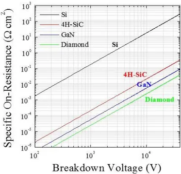
In Figure 2.5 the specific on resistance for the ideal drift region of a unipolar device is reported as a function of the breakdown voltage. In particular, the theoretical value of Si is compared with the ideal values of the wide band gap materials. For example, a typical Ron value of 1.4 cm2 obtained in a Si MOSFET becomes about 100 m cm2 for a 4H-SiC MOSFET [12]. In theory, 4H-SiC can reduce the resistance per unit area of the drift layer to 1/300 compared to Si at the same breakdown.
Chapter 2: Planar Power MOSFET for energy efficiency
32
Figure 2.5: Comparison of specific On-Resistance as a function of Breakdown Voltage
for unipolar devices on different materials.
Clearly, SiC exhibits a better trade-off between the Ron and breakdown voltage, which
allows to obtain a reduction of the power losses and an improvement of the energy efficiency in the power MOSFETs devices. Indeed, the static power dissipation, known as conduction loss, in the power semiconductors is primarily dependent on their on-resistance. The conduction loss is the loss from an on-resistance of the transistor that is generated when the drain current goes through the body diode during dead time. In order to get the average value of the conduction loss, simply multiply the on-resistance (Ron) for the drain current. The conduction power losses of the MOSFET as a function of the on resistance can be expressed as:
(2.7)
Notice that, Ion is the drain current when the MOSFET is on, and RDSon is the
drain-source resistance of the MOSFET when it is on. If the transistor is an ideal switch, there would be no conduction power loss. In order to reduce the conduction loss, on-resistance must be minimized. These aspects with Si technology result in an increase of the cost. Conversely, using 4H-SiC technology at the same breakdown voltage a
Chapter 2: Planar Power MOSFET for energy efficiency
35
Figure 2.8 reports a schematic structure of the power planar MOSFET with the resistance components [13].
Then, the total specific on-resistance is given by:
(2.8)
where RCS and RCD are the specific contact resistance of source and drain terminals,
respectively. In a first approximation, these contributions can be negligible. Moreover, the RCH is the channel resistance, RA is the accumulation region resistance, RJFET is the
resistance of the JFET region, RD is the resistance of the drift region after taking into
account current spreading from the JFET region and Rsubs is the resistance of the N+
substrate.
Figure 2. 8: Schematic structure of the planar MOSFET. In particular, in (a) the
geometrical components and in (b) the resistance components of Ron are reported.
These resistances can be analytically modelled. The drain current flows through a channel region with a small cross-section before entering the JFET region. The current spreads into the drift region from the JFET region at a 45 degree angle and then becomes uniform. The dimension of “a” is fixed by the alignment tolerance during the device fabrication that typically is around 0.5 µm. The channel resistance is given by:
Chapter 2: Planar Power MOSFET for energy efficiency
36
(2.9)
where LCH is the channel length as shown in Figure 2.7, µinv is the mobility for electrons
in the inversion layer channel, Cox is the specific capacitance of the gate oxide, VG is the
applied gate bias, and VTH is the threshold voltage.
Although an inversion layer mobility of 165 cm2V-1s-1 has been observed in lateral MOSFET structures in SiC [14], the inversion layer mobility in high voltage 4H-SiC power MOSFET structure [15] is usually much lower, i.e. in the range 10 –20 cm2V-1s-1.
The specific on – resistance contributed by the accumulation layer in a planar SiC MOSFETs is given by:
(2.10)
where the coefficient KA has been introduced to account for the current spreading from
the accumulation layer into the JFET region. A typical value for this coefficient is 0.6. In the case of n-channel 4H-SiC MOSFET structures, is the accumulation layer mobility; a typical values is almost 4 times the channel mobility. In particular, in the case of n-channel 4H-SiC MOSFET structures, accumulation layer mobility values of 100–200 cm2V-1s-1 have been experimentally observed [16]. Moreover, W
P is the “zero
bias” depletion width for the JFET region. The “zero bias” depletion width in the JFET region can be computed by using its doping concentrations on both sides of the junction and the built-in potential VPib:
√
(2.11)
The electrons entering from the channel into the drift region are distributed into the JFET region via the accumulation layer formed under the gate electrode. The current flow through the JFET region can be treated with a uniform current density. The specific on-resistance contributed by the JFET region in the planar SiC MOSFET structure can be obtained by using
Chapter 2: Planar Power MOSFET for energy efficiency
37
(
)
(2.12)where ρD is the resistivity of the JFET region given by
(2.13)
where µn is the bulk mobility appropriate to the doping level of the JFET region.
The resistance contributed by the drift region in the planar SiC MOSFET structure is enhanced above that of the ideal drift region due to current spreading from the JFET region. The drift region spreading resistance can be obtained by using:
(
)
(
)
(2.14)Finally, the substrate resistance contribution depends on the substrate resistivity and its thickness. This contribution is given by the relationship:
(2.15)
In Figure 2.9, the various on-resistance components have been modelled using the above analytic expression [2] for a 4H-SiC planar MOSFET, with a drift region doping concentration of 1016cm-3 and thickness of 20µm:
Chapter 2: Planar Power MOSFET for energy efficiency
39
Therefore, as a consequence of this behaviour, the on-resistance and, consequently, the on-state performances of SiC power MOSFETs are strongly limited by the channel resistance. In fact, the weakest building block in 4H-SiC MOSFETs technology is the channel fabrication.
2.3 Technology Issues for 4H-SiC MOSFET fabrication
Although the 4H-SiC MOSFET is considered to be significantly advantageous as compared to other types of power devices, some technical difficulties need to be overcome before it can achieve its full potential and it can replace silicon as the dominant semiconductor.
The persistent problems plaguing SiC device development are the realization of thermally stable Ohmic contacts to p-SiC with low resistivity and the notoriously low channel mobility in MOS devices. Both issues strongly impact the specific on – resistance of the devices. Not least, the gate oxide reliability under high temperature and high electric field is a fundamental open issue for SiC devices.
Regarding the Ohmic contact on p-type region, ion-implantation is the method of choice used for local doping of SiC [17, 2,18,19], since conventional diffusion techniques cannot be used, due to the small diffusivity of impurities in the material. As a matter of fact, ion-implantation doping of SiC is currently employed to fabricate several planar devices, like Schottky diodes, junction barrier Schottky (JBS) and metal-oxide-semiconductors field effect transistors (MOSFETs). However, in spite of the important and original progresses achieved in the last years, two closely linked physical issues still represent a concern for these devices, i.e., the p-type doping process by ion-implantation and the formation of Ohmic contacts on the implanted p-type regions. In particular, the reduction of the specific contact resistance of Ohmic contacts is required to minimize the total device series resistance (Ron) and, ultimately, to reduce the overall power
dissipation of single device and/or complex power modules.
While for n-type doping of SiC an almost complete electrical activation of the implanted dopant ions (i.e., Phosphorous) can be achieved already upon annealing at 1500°C [18,20], p-type doping (i.e., Aluminium) requires annealing at higher temperatures (T = 1500-1800°C) to promote the electrical activation of the dopant in


![Table 2.1 summarizes the figures of merit for n-type 4H-SiC, 3C-SiC, diamond [10], GaN [11], GaAs [11] and Si [11]](https://thumb-eu.123doks.com/thumbv2/123dokorg/4471806.31973/40.892.206.731.250.480/table-summarizes-figures-merit-type-sic-diamond-gaas.webp)
![Figure 2.8 reports a schematic structure of the power planar MOSFET with the resistance components [13]](https://thumb-eu.123doks.com/thumbv2/123dokorg/4471806.31973/44.892.176.774.515.901/figure-reports-schematic-structure-planar-mosfet-resistance-components.webp)