P
OLITECNICO DI
M
ILANO
S
CUOLA DI
I
NGEGNERIA DEI
S
ISTEMI
D
IPARTIMENTO DI
B
IOINGEGNERIA
LAUREA SPECIALISTICA
I
NGEGNERIA
B
IOMEDICA
A
SMART STRETCHABLE
M
ULTI-
E
LECTRODE
A
RRAY:
A FEASIBILITY STUDY
Supervisor for Politecnico di Milano:
Prof. Sergio CERUTTI
Co‐examiner for Philips Research Eindhoven
and Delft University of Technology:
Prof. Ronald DEKKER
Co-examiner for Politecnico di Torino:
Prof. Filippo MOLINARI
Thesis by:
Giuliano BUTTI
750514
ACADEMIC YEAR 2010/2011
TABLE OF CONTENTS
INDEX OF FIGURES ... 4 INDEX OF TABLES ... 11 SOMMARIO ... 12 ABSTRACT ... 19 1.INTRODUCTION ... 251.1 STRETCHABLE ELECTRONICS, A LITERATURE REVIEW ... 26
1.1.1 STRETCHABLE ELECTRODES ... 29
1.1.2 STIFF ISLANDS ONTO AN ELASTOMERIC SUBSTRATE ... 30
1.1.3 STRETCHABLE INTERCONNECTS ... 31
2.MATERIALS AND METHODS ... 36
2.1 STRENGTH OF MATERIALS ... 37
2.2 SUBSTRATE MATERIAL ... 38
2.3 POLYDIMETHYLSILOXANE ... 39
2.3.1 PREPARATION ... 40
2.3.2 MECHANICAL PROPERTIES ... 41
2.3.3 METAL THIN FILMS ON POLYMER SUBSTRATES ... 44
2.3.4 STERILIZATION AND EXPOSURE TO CULTURE MEDIA ... 47
2.4 SILICON OXIDE... 48 2.4.1 THERMAL OXIDE ... 48 2.4.2 PECVD OXIDE ... 48 2.5 STIFF ISLANDS ... 49 2.5.1 SILICON NITRIDE ... 50 2.5.2 POLY-SILICON ... 51 2.6 MICROFABRICATION FUNDAMENTALS ... 52 2.6.1 PHOTOLITHOGRAPHY ... 52 2.6.2 MASK DESIGN ... 52 2.6.3 SPIN-COATING ... 53 2.6.4 SOFT BAKING ... 54 2.6.5 EXPOSURE ... 54 2.6.6 DEVELOPING ... 55
2.6.7 POSTBAKING ... 55
2.6.8 RESIST STRIPPING... 55
2.6.9 ETCHING ... 56
2.6.10 WET CHEMICAL ETCHING ... 57
2.6.11 REACTIVE ION ETCHING ... 57
2.6.12 DEEP REACTIVE ION ETCHING ... 59
3.COMPLEMENTARY EXPERIMENTS ... 61
3.1 MASK DESIGN ... 62
3.2 FEM MECHANICAL SIMULATION... 64
3.2.1 MEMBRANE INFLATION ... 64
3.2.2 EFFECTS OF ISLAND’S SHAPE AND DIMENSIONS ... 70
3.2.3 ANTI-DELAMINATION SHIELD ... 71
3.3 BULGE TEST ... 74
3.3.1 BULGE TEST DEVICE ... 78
4.FABRICATION PROCESS ... 81
4.1 THERMAL OXIDE AS ETCH STOP LAYER ... 82
4.1.1 20 μm PDMS LAYER ... 86
4.1.2 80 μm PDMS LAYER ... 93
4.2 ZERO-STRESS PECVD OXIDE AS ETCH STOP LAYER ... 95
5.RESULTS………… ... 101
5.1 EFFECTS OF PDMS THICKNESS ... 102
5.2 EFFECTS OF ISLANDS’ SHAPE ... 105
5.2.2 EFFECTS OF ANTI-DELAMINATION STRUCTURES ... 108
6.APPLICATIONS OF STRETCHABLE ELECTRONICS ... 110
6.1 STRETCHABLE MEA FOR CARDIO-TOXICITY DRUG SCREENING APPLICATIONS ... 111
6.1.1 PATTERNING CELLS ON THE MEMBRANE ... 120
6.1.2 ADVANTAGES OF STRETCHABILITY ... 122
6.2 IMPLANTABLE DEVICES ... 125
7.CONCLUSIONS ... 130
REFERENCES ... 134 APPENDIX A – DETAILED FABRICATION SEQUENCE
4 INDEX OF FIGURES
INDEX OF FIGURES
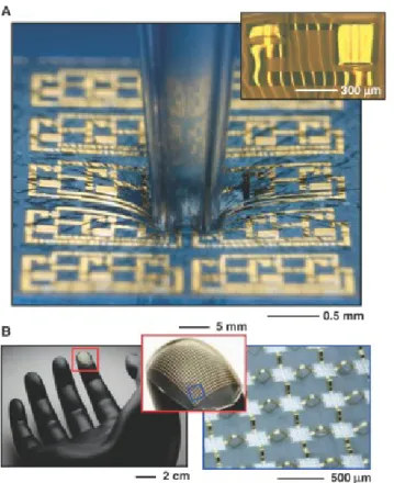
FIGURE 1.1-EXAMPLES OF STRETCHABLE ELECTRONICS.A)STRETCHABLE SILICON CIRCUIT IN A WAVY GEOMETRY, COMPRESSED IN ITS CENTER BY A GLASS CAPILLARY TUBE (MAIN) AND WAVY LOGIC GATE BUILT WITH TWO TRANSISTORS (TOP RIGHT INSECT).B)STRETCHABLE SILICON CIRCUIT WITH A MESH DESIGN, WRAPPED ONTO A MODEL OF A FINGERTIP, SHOWN AT LOW (LEFT), MODERATE (CENTER) AND HIGH (RIGHT) MAGNIFICATION.THE RED (LEFT) AND BLUE (CENTER) BOXES INDICATE THE REGIONS OF MAGNIFIED VIEWS IN THE CENTER AND RIGHT, RESPECTIVELY.THE IMAGE ON THE RIGHT WAS COLLECTED WITH AN AUTOMATED CAMERA SYSTEM THAT COMBINES IMAGES AT DIFFERENT FOCAL DEPTHS TO ACHIEVE A LARGE DEPTH OF FIELD [2] ... 26
FIGURE 1.2-CONCEPTS FOR STRETCHABLE ELECTRONIC MATERIALS.A) STRETCHABLE SILICON MEMBRANE
(~100 NM THICKNESS) CONFIGURED IN A WAVY SHAPE AND BONDED TO A PIECE OF RUBBER, PRESENTED IN OPTICAL (TOP) AND ATOMIC FORCE (BOTTOM) MICROSCOPE IMAGES.B)EXTREMELY STRETCHABLE SILICON MEMBRANE (~100-NM THICKNESS) PATTERNED INTO A MESH GEOMETRY AND BONDED TO A RUBBER SUBSTRATE ONLY AT SQUARE PADS LOCATED BETWEEN ARCSHAPED BRIDGE STRUCTURES, PRESENTED IN MODERATE (TOP) AND HIGH (BOTTOM) MAGNIFICATION SCANNING ELECTRON MICROSCOPE
(SEM) IMAGES.THE PDMS IS COLORIZED BLUE [2] ... 27 FIGURE 1.3-SCHEMATIC ILLUSTRATION OF THE PROCESS FOR BUILDING STRETCHABLE SINGLE-CRYSTAL SI
DEVICES ON ELASTOMERIC SUBSTRATES [7] ... 28
FIGURE 1.4-SCANNING ELECTRON MICROGRAPHS OF A 100 NM THICK AU LAYER ON A PDMS SUBSTRATE.
MICROSCOPIC CRACKS THAT FORM IN THE FILM CAN TAKE PLACE DURING FABRICATION [9] ... 29
FIGURE 1.5-TOP: SCHEMATIC CROSS-SECTION ILLUSTRATING A COMPLIANT ELECTRODE OBTAINED BY ION IMPLANTATION.THE CLUSTERS ARE TOUCHING EACH OTHER BUT CAN SLIDE RELATIVE TO EACH OTHER.
THEY CAN SUSTAIN LARGE STRAIN WHILE REMAINING CONDUCTIVE.BOTTOM: NON-COMPLIANT ELECTRODE OBTAINED BY THIN-fiLM DEPOSITION.THE STRONG BINDING FORCES WHICH LINK THE METALLIC ATOMS TOGETHER DRASTICALLY LIMIT THE ACHIEVABLE STRAIN BEFORE DAMAGE TO THE ELECTRODE [11] ... 30
FIGURE 1.6-A COMPLIANT, ELASTOMERIC SUBSTRATE CARRIES STIFF SUBCIRCUIT ISLANDS INTERCONNECTED WITH STRETCHABLE METALLIZATION.UPON DEFORMATION, THE SUBSTRATE ALONG WITH THE
STRETCHABLE INTERCONNECTS ACCOMMODATES THE RESULTING TENSILE, COMPRESSIVE, AND SHEAR STRAINS WHILE THE ISLANDS REMAIN INTACT [3] ... 30
FIGURE 1.7-ARCHITECTURE OF AN ELASTIC ELECTRONIC SURFACE MADE ON A POLYMER SUBSTRATE.ACTIVE DEVICE CELLS CAN BE FABRICATED ON RIGID SUBCIRCUIT ISLANDS DISTRIBUTED OVER THE POLYMER SURFACE.THE CELLS ARE INTERCONNECTED WITH STRETCHABLE METALLIZATION [12]... 31
FIGURE 1.8-STRESS DISTRIBUTION IN COPPER CONDUCTOR LINE FOR THREE DIFFERENT CONDUCTOR SHAPES
[14] ... 32 FIGURE 1.9-POISSON EFFECT OBSERVED DURING A UNIAXIAL TENSION TEST [15] ... 33
5
INDEX OF FIGURES
FIGURE 1.10-TENSILE STRAIN TEST OF HORSESHOE METAL INTERCONNECTS.A)BEFORE ELONGATION.B)
AFTER 25% ELONGATION HIGHLIGHTING THE FAILURES IN THE CREST AND TROUGH ... 33 FIGURE 1.11-SEM MICROGRAPH OF THE AS-PREPARED 25 NM THICK GOLD FILM ON PDMS.THE GOLD
LIGAMENTS PERCOLATE BETWEEN THE MICRON-SIZE MICRO-CRACKS [10] ... 35
FIGURE 2.1–A)A MATERIAL BAR WITH LENGTH L0 AND CROSS SECTION AREA A0.B)IF A LOAD F IS APPLIED TO
BOTH ENDS OF THE BAR, IT IS STRETCHED TO A NEW LENGTH L AND ITS CROSS SECTION AREA SHRINKS TO
A[18] ... 37 FIGURE 2.2–A SCHEMATIC ILLUSTRATION OF THE STRESS-STRAIN CURVE OF A METAL AND A POLYMER [18] . 38 FIGURE 2.3:A)CHEMICAL STRUCTURE OF SILICONE MONOMER;B)SPACE FILLING MODE OF A PDMS CHAIN
[19] ... 39 FIGURE 2.4-GRAPH OF THE YOUNG'S MODULUS WITH RESPECT TO CURING TEMPERATURE FOR PDMS WITH A
10:1 AND 11:1 WEIGHT RATIO OF PREPOLYMER TO HARDENER [34] ... 41
FIGURE 2.5-GRAPH OF THE YOUNG'S MODULUS A) WITH RESPECT TO THE WEIGHT RATIO OF PDMS
PREPOLYMER TO HARDENER FOR SAMPLES CURED AT 85°C FOR 100 MINUTES B) WITH RESPECT TO TIME AGED AT 100°C IN AN AIR OVEN FOR PDMS WITH A 10:1 AND 11:1 WEIGHT RATIO OF PREPOLYMER TO HARDENER [34] ... 42 FIGURE 2.6-ELASTIC MODULUS OF SYLGARD 184A) AGAINST TEMPERATURE B) AS A FUNCTION OF THE
STRAIN RATE [35] ... 42
FIGURE 2.7-YOUNG'S MODULUS VERSUS THE INVERSE OF PDMS THICKNESS, T-1/2(ΜM-1/2).THE TRANSITION
POINT FROM SIZE DEPENDENT TO BULK BEHAVIOR IS PREDICTED TO BE AROUND 200 ΜM IN THICKNESS OF
PDMS MEMBRANE [32] ... 43 FIGURE 2.8-A)SKETCH OF THE PDMS MIXTURE DISPENSED ONTO A WAFER SUBSTRATE AND TANGLED
POLYMER CHAIN COILS.B) WHEN SPINNING IS APPLIED THE PDMS IS THINNED AND POLYMER CHAIN COILS ARE STRETCHED BY SHEAR STRESS WHICH IS A GRADIENT ALONG THE THICKNESS (Z) DIRECTION.C) WHEN A GREATER SPIN SPEED IS APPLIED THE POLYMER CHAINS ARE EXTENSIVELY REORDERED IN THE RADIAL DIRECTION AND THE PDMS MEMBRANE IS THINNED FURTHER.D) THE PDMS MEMBRANE WITH A DESIRED THICKNESS AND REORDERED (ALIGNMENT) IS SEPARATED FROM THE WAFER SUBSTRATE [32] 43
FIGURE 2.9-THE RAPTURE OF A METAL FILM CAUSED BY STRAIN LOCALIZATION.ANECKING OF A FREE STANDING METAL FILM,B LOCAL ELONGATION IS SUPPRESSED BY THE SUBSTRATE [40] ... 44 FIGURE 2.10-FOCUSED ION BEAM (FIB) IMAGES OF (A) AS-DEPOSITED FILM AND, AND (B) FILM ANNEALED AT
200°C FOR 30 MIN.ANNEALING HAS CAUSED SIGNIFICANT GRAIN GROWTH.WHEREAS GRAINS HAVE A RELATIVELY UNIFORM DISTRIBUTION IN THE ANNEALED FILM, ISOLATED LARGE GRAINS CAN BE IDENTIFIED IN THE AS-DEPOSITED FILM [39] ... 45
FIGURE 2.11-THE RESISTANCE CHANGE VERSUS ELONGATION NORMALIZED WITH THEIR INITIAL VALUES.THE CURVE R/R0=(L/L0)2 SHOWS THE THEORETICAL PREDICTION OF RESISTANCE CHANGE ASSUMING THAT NO CRACKS HAPPEN IN THE FILM.THE RESISTANCE OF THE AS-DEPOSITED FILM STARTS TO DEVIATE SIGNIFICANTLY FROM THE THEORETICAL PREDICTION DUE TO EMERGING CRACKS AT ELONGATION OF APPROXIMATELY 12%, WHEREAS THE ANNEALED FILM IS MUCH MORE ROBUST [39] ... 46
FIGURE 2.12-ASCHEMATIC ILLUSTRATION OF CONCURRENT FAILURE PROCESSES: DEFORMATION-ASSOCIATED GRAIN GROWTH, STRAIN LOCALIZATION PROMOTED BY LARGE GRAINS, AND FILM/SUBSTRATE INTERFACE
6 INDEX OF FIGURES
DEBONDING.THE THREE PROCESSES COEVOLVE TO FORM A NECK.FIB IMAGES OF UNANNEALED FILM:B
NOT STRETCHED,C15%, AND D20% OF STRETCH [39] ... 46
FIGURE 2.13-THE EFFECT OF PEAK THERMAL CYCLING TEMPERATURE ON THE ROOM TEMPERATURE STRESS OF SILANE-BASED PECVD OXIDE FILMS [43]... 49
FIGURE 2.14-SCHEMATIC DIAGRAM FOR MEASURING DETACHMENT LENGTH AND ADHESION ENERGY OF PDMS MICROSTRUCTURES.THE SURFACE UNDER TESTING (S.O.T.) INCLUDE SINGLE CRYSTAL SILICON, THERMALLY GROWN OXIDE,LPCDVNITRIDE, GLASS AND PDMS[46] ... 50
FIGURE 2.15–DEPOSITION RATE AS A FUNCTION OF GAS-FLOW RATIO FOR A TEMPERATURE OF 850˚C AND A PRESSURE FOR A GAS-FLOW RATIO NH3/SIH2CL2 OF 30/170[44] ... 50
FIGURE 2.16-ETCH RATE OF SILICON NITRIDE IN A PARALLEL-PLATE PLASMA ETCHER AS A FUNCTION OF PROCESS GAS-flOW RATIO FOR A DEPOSITION TEMPERATURE OF 850˚C AND A PRESSURE OF 20PA.THE PLASMA ETCHING WAS PERFORMED USING A GAS COMPOSITION OF CHF37.5 SCCM AND N242.5 SCCM, R.F. POWER (FREQUENCY 13.56MHZ) AND GAS PRESSURE OF 60W(52 MW/CM3) AND 5PA, RESPECTIVELY [44] ... 51
FIGURE 2.17–A TYPICAL STRESS BIAXIAL-STRAIN PLOT [47] ... 51
FIGURE 2.18-ANGULAR VIEW OF ALIGNMENT MARKS ETCHED IN SI (SEM MICROGRAPH) ... 53
FIGURE 2.19-PERSISTS OF POSITIVE AND NEGATIVE PHOTORESISTS AFTER DEVELOPMENT ... 55
FIGURE 2.20-ETCH PROFILES (A) ISOTROPIC ETCH PROFILE (B) ABSOLUTE AN-ISOTROPIC ETCH PROFILE ... 56
FIGURE 2.21- ETCH (BLACK) AND PASSIVATION (PINK) STEPS OF DRIE ... 59
FIGURE 2.22-TYPICAL PROFILE OF DEEP REACTIVE ION ETCHING (SEM MICROGRAPH).EACH RIPPLE SHOWS ONE COMPLETE CYCLE (ETCHING AND PASSIVATION) ... 59
FIGURE 3.1:THREE DIFFERENT ISLAND SHAPES HAVE BEEN TESTED, VARYING THEIR DIMENSIONS AND THE DISTANCE BETWEEN THEM ... 62
FIGURE 3.2-SNAPSHOT FROM CADENCE.A) A VIEW OF SOME CHIPS.THE GREY LINE AROUND THEM FIX THE BORDERS OF EACH CHIP (1 CM X 1 CM) FOR THE BACKSIDE MASK,LIGHT GREEN SHAPE IN THE CENTER OF EACH CHIP REPRESENT THE HOLE AND DARK GREEN STRUCTURES INSIDE THE HOLE ARE THE ISLANDS OF THE FIRST TOPSIDE MASK.ALSO A CODE ALLOWS US TO DISTINGUISH THE CHIP DURING THE MICROSCOPE INSPECTION.THE FIRST PART INDICATES THE DIMENSION OF THE ISLAND (S FOR 50 µM,M FOR 100 µM,L FOR 200 µM AND XL FOR 300 µM ISLANDS).THE SECOND PART INDICATES THE SHAPE OF THE ISLAND (C FOR CIRCLE,Q FOR SQUARE AND CQ FOR ROUNDED SQUARE).THE LAST NUMBER INDICATES THE INTERISLAND SPACE (IN µM).B) A DETAILED VIEW OF SOME ISLANDS (BLUE) SURROUNDED BY THE ANTI -DELAMINATION SHIELD (RED)... 63
FIGURE 3.3-THE ONE-ISLAND MEMBRANE THAT HAS BEEN INFLATED IN THE FIRST SIMULATION ... 65
FIGURE 3.4-USER DEFINED MESH.A)THE OVERALL MESH IS PRESENTED IN THE 3D STRUCTURE.AS EXPLAINED BEFORE, WE DEFINED THE MESH ON THE TOP SURFACE AND SWEPT IT THROUGH THE WHOLE THICKNESS OF THE MEMBRANE.B)TOP VIEW OF THE MESH.IN THE CORNERS OF THE ISLAND THE ELEMENTS BECOME SMALLER AND THE ACCURACY HIGHER.C)A DETAIL OF THE CORNER, THE ISLAND IS HIGHLIGHTED IN RED ... 66
FIGURE 3.5-FIRST PRINCIPAL STRAIN IN THE MEMBRANE INFLATED FROM THE BACKSIDE WITH A 70KPA PRESSURE.A)A THREE-DIMENSIONAL VIEW OF THE DEVICE.AS EXPECTED THE HIGHER STRAIN ARE IN THE
7
INDEX OF FIGURES
REGION SURROUNDING THE STIFF ISLAND ALONG THE Y AXIS.B)THE FRONTAL VIEW OF THE MEMBRANE.
WE CAN SEE THE SHAPE OF THE SUBSTRATE ONCE THE PRESSURE IS APPLIED.HIGHER STRAIN IS ALSO AT THE BOTTOM SIDES OF THE MEMBRANE, POSSIBLE CAUSE OF DELAMINATION OF THE SUBSTRATE FROM THE SURROUNDING ... 68
FIGURE 3.6-A VIEW ON THE SECOND (A) AND THIRD (B) PRINCIPAL STRAIN.STRAIN IS A VECTOR THAT CAN BE COMPLETELY DESCRIBED WITH THREE ORTHOGONAL COMPONENTS.HOWEVER, AS WE CAN SEE IN THESE PICTURES, THE VALUES OF THESE TWO COMPONENTS ARE REALLY LOWER COMPARED TO THE FIRST ONE.IN A FIRST APPROXIMATION WE CAN CONSIDER JUST THE FIRST PRINCIPAL STRAIN SHOWED IN ... 69 FIGURE 3.7-FIRST PRINCIPAL STAIN IN THE PROXIMITY OF THE ROUND ISLAND.PHYSICAL DEFORMATION IS
INCLUDED IN THESE PLOTS [19] ... 70
FIGURE 3.8-FIRST PRINCIPAL STAIN IN THE PROXIMITY OF THE ROUND ISLAND FOR DIFFERENT ISLAND SHAPES
(RFILLET) VARYING THE ISLAND SIZE L.PHYSICAL DEFORMATION IS INCLUDED IN THESE PLOTS [19] ... 71
FIGURE 3.9-SCANNING ELECTRON MICROSCOPE (SEM) PICTURES OF THE INFLATED MEMBRANE.A)
DELAMINATION AROUND ISLANDS IS DUE TO THE HIGH STRAIN IN THE ELASTOMERIC MEMBRANE THAT IS SURROINDING THE STIFF MATERIAL B)A DETAIL OF THE SAME DELAMINATION.A SMALL VALLEY IN THE
PDMS TAKES PLACE AT THE EDGES OF THE ISLAND ... 72 FIGURE 3.10–TWO-DIMENSIONAL VIEWS OF THE MEMBRANE CROSS SECTION ONCE A 70KPA PRESSURE IS
APPLIED FROM THE BACKSIDE.SYMMETRY CONDITION IS IMPOSED ALONG THE VERTICAL AXIS, ALLOWING A MORE ACCURATE SIMULATION OF THE FIRST PRINCIPAL STRAIN.SECOND AND THIRD PRINCIPAL STRAINS ARE NOT REPORTED IN THIS STUDY, THEIR VALUES ARE EXTREMELY LOWER COMPARED TO THE FIRST PRINCIPAL ONE.THREE DIFFERENT CONFIGURATIONS HAVE BEEN ANALYZED, WITHOUT ANY INDENTATION
(A),4 µM INDENTATION (B) AND 8 µM INDENTATION (C).THE SHAPE OF THE MEMBRANE WHEN NO PRESSURE IS APPLIED IS SHOWED WITH A BLACK LINE BENEATH THE INFLATED MEMBRANE. ... 73
FIGURE 3.11–A DETAIL OF THE INFLATED MEMBRANE SURROUNDING THE ISLAND.WITH AN 8 µM INDENTATION (B) THE MAXIMUM STRAIN IS REDUCED BY 54% COMPARED TO THE BASE CONDITION WITHOUT ANY INDENTATION (A) ... 74 FIGURE 3.12-BULGE TEST PRINCIPLE:A) A FREE-STANDING MEMBRANE (IN GREY) ON A RIGID SUBSTRATE (IN
BROWN) WITH AN INITIAL LENGTH L.B) SIDE VIEW OF THE STACK, STIFF ISLANDS ARE REPRESENTED WITH BLUE RECTANGLES.C)AS PRESSURE IS APPLIED, THE PLANAR MEMBRANE TRANSFORM INTO A CYLINDRICAL CUP WITH HEIGHT H0 AND THE ELASTOMERIC SUBSTRATE ELONGATES TO A NEW LENGTH L1. ... 75 FIGURE 3.13-CROSS SECTION OF TWO DIFFERENT MEMBRANES WITH DIFFERENT ISLANDS SIZE, BEFORE AND
AFTER STRETCHING.THE ELASTOMERIC MEMBRANE IS REPRESENTED IN DARK BLUE AND THE ISLANDS ARE DEPICTED IN LIGHT BLUE.NOTWITHSTANDING THE INITIAL AND THE FINAL LENGTH OF THE TWO
MEMBRANES ARE THE SAME, THE HYPOTHESIS THAT STIFF ISLANDS DO NOT DEFORM REQUIRES, IN CASE OF BIG ISLANDS, A HIGHER PERCENTAGE STRAIN OF THE ELASTOMERIC SUBSTRATE. ... 76
FIGURE 3.14-CYLINDRICAL MODELING OF THE MEMBRANE INFLATION. A CROSS-SECTIONAL VIEW ... 77
FIGURE 3.15-THE BULGE TEST DEVICE MOUNTED ON A MICROSCOPE PLATE.TWO CABLES CONNECTED ON THE SIDES PROVIDE THE VACUUM CLAMPING AND THE INFLECTION RESPECTIVELY.THE WHITE BLOCKS ON THE TWO SIDES OF THE CHIP ALLOW A CORRECT POSITIONING OF THE CHIP ITSELF... 79
8 INDEX OF FIGURES
FIGURE 3.16-A CROSS SECTIONAL VIEW OF THE TESTING DEVICE.THE GREEN LAYER ON TOP OF SILICON
SUBSTRATE (IN GREY) REPRESENTS THE INFLATED MEMBRANE. ... 79
FIGURE 3.17-AN OVERALL VIEW OF THE EXPERIMENTAL SET USED TO APPLY PRESSURE ON THE CHIPS AND COLLECT INFORMATION OF THEIR BEHAVIOR UNDER STRESS ... 80
FIGURE 4.1-COMPLETE FABRICATION PROCESS SEQUENCE ... 83
FIGURE 4.2-SPIN CURVE FOR HPR504 RESIST [56] ... 84
FIGURE 4.3–50 µM CIRCLED SQUARED ISLANDS WITH 100 µM INTERISLAND SPACE ... 85
FIGURE 4.4-A DETAIL OF ONE 50 µM CIRCLED SQUARED ISLAND AFTER RESIST DEVELOPMENT ... 85
FIGURE 4.5-10 µM GROOVES ON THE BACKSIDE DESIGNED TO FACILITATE THE SPLITTING OF THE CHIPS AT THE END OF THE FABRICATION PROCESS ... 86
FIGURE 4.6-ALUMINUM WRINKLES ON PDMS SEEN FROM INCREASING MAGNITUDES ... 87
FIGURE 4.7-WRINKLES ON ALUMINUM AND SILICON OXIDE LAYERS AFTER SILICON IS DRY ETCHED FROM THE BACKSIDE.ACCORDING TO THE DIRECTION OF THE STRESS IN THE MEMBRANE, THESE WRINKLES PROPAGATES HORIZONTALLY, VERTICALLY OR SINUSOIDALLY ... 88
FIGURE 4.8-A SCHEMATIC OF THE MEMBRANE.IN THIS EXAMPLE STRESS IS SUPPOSED TO BE RELEASED HORIZONTALLY.THEREFORE ALUMINUM FORMS ITS WRINKLES VERTICALLY ON THE TOP OF THE MEMBRANE ... 89
FIGURE 4.9-CRACKS ON THE MEMBRANE.THESE CRACKS ARE OFTEN PERPENDICULAR TO THE WRINKLES OF THE MEMBRANE.AS EXPLAINED BEFORE IN THIS CASE THE MEMBRANE WAS ABLE TO RELEASE ITS COMPRESSIVE STRESS JUST IN ONE DIRECTION, CAUSING BENDING OF THE MEMBRANE (DESCRIBED BY WRINKLES ON THE TWO EXTREMITY SURFACES) AND CRACKS IN THE OTHER DIRECTION. ... 90
FIGURE 4.10-MOLECULAR STRUCTURE OF TRITON X-100[57] ... 90
FIGURE 4.11-ELASTOMERIC SUBSTRATE AFTER BOE ETCHING PREVIOUSLY TREATED WITH TRITON X-100. WRINKLES ARE ALL OVER THE SURFACE [100X MAGNIFICATION] ... 91
FIGURE 4.12-MEMBRANE INSPECTION AFTER REMOVAL OF SILICON OXIDE.NO MORE WRINKLES ARE PRESENT; THE OXIDE LAYER HAS BEEN COMPLETELY REMOVED ... 91
FIGURE 4.13-AFTER BOE ETCHING THE SILICON OXIDE HAS BEEN COMPLETELY REMOVED FROM THE CENTER OF THE HOLE BUT NOT AROUND THE EDGES.DIFFERENT COLORS OF THE ISLANDS REFER TO DIFFERENT THICKNESS OF THE OXIDE LAYER STILL PRESENT ABOVE ... 92
FIGURE 4.14-INSPECTION OF THE MEMBRANE AFTER SILICON PLASMA EXPOSURE AND BOE ETCHING.NO MORE WRINKLES AFFECT THE MEMBRANE; THE ENTIRE SILICON OXIDE LAYER HAS BEEN REMOVED ... 92
FIGURE 4.15-DIRTY SPOTS IN THE CORNER OF THE EDGES.IN ORDER TO INSPECT THE ROLE OF THE SURFACTANT IN THE FORMATION OF THESE SPOTS WE REPEATED THE EXPERIMENT USING WATER IN PLACE OF IT ... 93
FIGURE 4.16–A)NO MORE WRINKLES AFFECT THE MEMBRANE B)NO DIRTY SPOTS ARE NOW IN PROXIMITY OF THE CORNERS, SHOWING THAT THEIR FORMATION IN THE PREVIOUS EXPERIMENT WAS MOSTLY DUE TO THE REACTIONS THAT TAKE PLACE WITH THE SURFACTANT ... 93
FIGURE 4.17-SPIN CURVE OF RTV615 AND SYLGARD 184, MEAN ACROSS THE WHOLE WAFER AREA [31] .... 94
FIGURE 4.18–COMPARISON BETWEEN ALUMINUM WRINKLES ABOVE 80 µM (A) AND 20 µM (B)PDMS LAYER ... 94
9
INDEX OF FIGURES
FIGURE 4.19-AN OVERALL VIEW OF THE 80 UM THICK PDMS MEMBRANE AFTER ALUMINUM AND OXIDE REMOVAL.IN THIS CASE NOR WRINKLES NEITHER CRACKS TOOK PLACE ON THE MEMBRANE ... 95 FIGURE 4.20-COMPLETE FABRICATION PROCESS SEQUENCE FOR NITRIDE ISLANDS.VARIATIONS FOR POLY
-SILICON WILL BE DESCRIBED IN THE CHAPTER ... 96
FIGURE 4.21-CIRCLE ISLANDS SURROUNDED BY A THIN LAYER OF RESIST.AT THE END OF THE FABRICATION PROCESS, ONCE THIS RESIST WILL BE REMOVED, THE INDENTATION WILL REMAIN IN THE MEMBRANE, REDUCING THE STRAIN IN THE PDMS AROUND THE ISLANDS AS SHOWED IN THE FEM PARAGRAPH ... 98
FIGURE 4.22-ELASTOMERIC SUBSTRATES AFTER SILICON REMOVAL.A)AN OVERALL IMAGE OF THE MEMBRANE SHOWS NEITHER WRINKLES NOR CRACKS TOOK PLACE IN OXIDE,PDMS AND ALUMINUM LAYERS.
PICTURES B) AND C) SHOW DETAILS ABOUT ISLANDS AND THE ANTI-DELAMINATION SHIELD
SURROUNDING THEM... 99 FIGURE 4.23-SEM PICTURES OF THE ANTI-DELAMINATION SHIELD SURROUNDING THE ISLANDS.A)AN
OVERALL VIEW OF THE ISLANDS SURROUNDED BY THESE CHANNELS.B)A DETAIL OF ONE CORNER; THE ISLAND IS SURROUNDED BY A SMALL PDMS LAYER (5 µM LENGTH) BEFORE THE INDENTATION.THE SIZE OF THE INDENTATION IS 10 µM AND ITS DEPTH IS 7.87 µM (THE SAME THICKNESS OF THE RESIST SPIN COATED IN THE INDENTATIONS AND THEN REMOVED WITH ACETONE) ... 100 FIGURE 5.1:LOCATIONS OF EDGE BEAD FORMED DURING THE SPIN-COATING OF PDMS ON TOP OF THE WAFER
... 102 FIGURE 5.2–STRAIN-TREND IN PDMS FOR TWO DIFFERENT MEMBRANE THICKNESSES WHEN THE SAME
PRESSURE IS APPLIED TO THE SAME ISLANDS CONFIGURATION.VERTICAL BARS INDICATE THE STANDARD DEVIATION OUT OF 15 MEASURES ... 103 FIGURE 5.3-SEM PICTURES OF PDMS SCRATCHING IN THE REGIONS BETWEEN THE ISLANDS ... 104
FIGURE 5.4-TRUE STRESS VERSUS TRUE STRAIN OF PDMS MEMBRANE WITH DIFFERENT THICKNESSES [32]
... 105 FIGURE 5.5-DISTRIBUTION OF THE FIRST PRINCIPAL STRAIN IN THE PDMS MEMBRANE SURROUNDING THE
ISLAND ACCORDING TO THE ISLAND SHAPE [19] ... 106 FIGURE 5.6-300 µM NITRIDE CIRCLE ISLAND INFLATED BY 65KPA (A) AND 80KPA (B).HUGE
DELAMINATION FROM THE SURROUNDING MEMBRANE TOOK PLACE ... 107
FIGURE 5.7-300 µM NITRIDE SQUARE ISLAND INFLATED BY 65KPA (A) AND 80KPA (B).DELAMINATION IS QUITE CONFINED ... 107
FIGURE 5.8-CIRCLE ISLAND (300 ΜM) WITH (B) AND WITHOUT (A) ANTI-DELAMINATION STRUCTURE.SAME PRESSURE IS APPLIED (80KPA).THE ANTI-DELAMINATION SHIELD PROVED TO REDUCE SIGNIFICANTLY THIS PHENOMENON ... 108
FIGURE 6.1-ELECTROPHYSIOLOGICAL DIFFERENCES BETWEEN ADULT HUMAN AND MOUSE CMS.HUMAN AND MOUSE HEARTS DISPLAY UNIQUE ECG PROFILES, WITH THE QT INTERVAL IN HUMANS APPROXIMATELY FIVE TIMES LONGER THAN IN MICE.THIS IS ALSO REFLECTED IN THE DIFFERENT AP DURATIONS AND SHAPES OF THE VENTRICULAR CMS FROM THESE TWO SPECIES AND IS DUE TO THEIR INSTINCTIVE IONIC CURRENTS.ALTHOUGH THE INWARD NA+ AND CA2+ CURRENTS (IN
A AND ICAL, RESPECTIVELY) ARE
COMPARABLE BETWEEN MOUSE AND HUMAN CMS, MAJOR DIFFERENCES ARE OBSERVED IN THE VARIOUS OUTWARD K+ CURRENTS (IN BLUE), WHICH PLAY DISTINCT ROLES IN HUMAN AND MOUSE AP
10 INDEX OF FIGURES
REPOLARIZATION.THE IKS AND IKR ARE THE MAJOR REPOLARIZING CURRENTS IN HUMAN CMS, WHEREAS IN
MICE I TO IS THE PREDOMINANT CURRENT.ADDITIONALLY IK,SLOW1,IK,SLOW2 AND ISS CONTRIBUTE TO
REPOLARIZATION IN MOUSE CMS, BUT ARE ABSENT FROM HUMAN VENTRICULAR CMS.THE APS AND THEIR UNDERLYING IONIC CURRENTS ARE ALIGNED WITH THEIR APPROXIMATE TIME OF ACTION DURING
THE QT INTERVAL SHOWN IN THE ECG EXAMPLES.(MS, MILLISECOND)[61] ... 112
FIGURE 6.2-QT-INTERVAL PROLONGATION SHOWN ON THE CARDIAC ACTION POTENTIAL [64] ... 113
FIGURE 6.3–TYPICAL PAUSE DEPENDENT TORSADE DE POINTES (TDP).THE TACHYARRHYTHMIA IS PRECEDED BY VENTRICULAR BIGEMINY, CREATING A SERIES OF “LONG” AND “SHORT” CYCLES (MARKED L AND S).THE LONG QT INTERVAL IS DIFFICULT TO APPRECIATE BECAUSE THE EXTRA-SYSTOLES CONCEAL THE TERMINAL PART OF THE QT SEGMENT.[65] ... 114
FIGURE 6.4-FIELD POTENTIAL RECORDINGS FROM A CARDIOMYOCYTE CLUSTER WITHIN AN EMBRYOID BODY PLATED ONTO A MEA.A) ELONGATED BEATING CELL CLUSTER AT DAY 6 AFTER PLATING THE EB. DIRECTION OF CONTRACTION SPREAD (MICROSCOPIC OBSERVATION) IS SHOWN BY ARROWS; RECORDING ELECTRODES ARE MARKED AS CIRCLES.B) SYNCHRONOUS RECORDINGS FROM ELECTRODES LABELED IN A. THE SEQUENTIAL INCREASE OF DELAY BETWEEN SPIKES REGISTERED AT ELECTRODES 45,56, AND 87 VERSUS ELECTRODE 34 CONFIRMS THE DIRECTION OF THE EXCITATION WAVE INDICATED BY ARROWS IN A. DATA RETRIEVED FROM THE RESEARCH OF [68] ... 117
FIGURE 6.5-FRESHLY PLACED EMBRYOID BODIES ON A 60 ELECTRODES MEA[68] ... 118
FIGURE 6.6-A CONFIGURATION FOR THE OVERALL SET-UP FOR DRUG SCREENING PROPOSED BY [1] ... 120
FIGURE 6.7- MICRO-CONTACT PRINTING FOR CELL ALIGNMENT PROCEDURE [76]... 121
FIGURE 6.8-CARDIAC MYOCYTES CULTURED ON TEXTURED MICROCHANNELS AND UNTEXTURED SILICONE [71] ... 122
FIGURE 6.9-FLUORESCENCE IMAGE OF HESC-DERIVED CARDIOMYOCYTES GROWN ON PDMS SUBSTRATE. COURTESY OF LEIDEN UNIVERSITY MEDICAL CENTRE ... 124
FIGURE 6.10-FLUORESCENCE IMAGE OF HESC-DERIVED CARDIOMYOCYTES GROWN ON PETRI-DISH (GLASS SUBSTRATE).COURTESY OF LEIDEN UNIVERSITY MEDICAL CENTRE ... 124
FIGURE 6.11-COMPONENTS OF A COCHLEAR IMPLANT SYSTEM.COURTESY OF MED-ELMEDICAL ELECTRONICS GMBH,INNSBRUCK,AUSTRIA [78] ... 126
FIGURE 6.12-PLACEMENTS AND COMPONENTS OF ENVISIONED NEXT-GENERATION INTRAOCULAR RETINAL PROSTHESIS [80] ... 127
FIGURE 6.13-PARYLENE MEAS TACKED TO THE RIGHT CANINE RETINA SHOWING NORMAL VESSEL PERFUSION UNDER THE ARRAYS.ARROWS POINT TO THE RETINAL TACK [80] ... 127
FIGURE 6.14-HEAT MOLDED AND ANNEALED RETINAL ELECTRODE ARRAY WITH RETAINED SPHERICAL CURVATURE (ARROW DENOTES RETINAL TACK HOLE)[80] ... 128
FIGURE 6.15-SIMPLIFIED SCHEMATIC OF SUBCORTICAL MOTOR SYSTEM CIRCUITRY.BLUE ARROWS REPRESENT EXCITATORY SYNAPSES, AND OPEN RED CIRCLES REPRESENT INHIBITORY SYNAPSES.DOTTED LINE ACROSS THE THALAMUS INDICATES THE SEGREGATION BETWEEN STRIATAL AND CEREBELLAR CONNECTIONS.CBL CTX, CEREBELLAR CORTEX;CBLNUC, CEREBELLAR NUCLEI;GPE, GLOBUS PALLIDUS EXTERNAL SEGMENT;GPI, GLOBUS PALLIDUS INTERNAL SEGMENT;PN, PONTINE NUCLEI;SNL, SUBSTANTIA NIGRA PARERETICULATE;STN, SUBTHALAMIC NUCLEUS;STR, STRIATUM;THAL, THALAMUS [81] ... 129
11
INDEX OF TABLES
INDEX OF TABLES
TABLE 1.1-PROPERTIES OF THE MATERIALS INVOLVED IN THE STUDY FROM [16] ... 34
TABLE 2.1-SCORING CARD FOR THREE CANDIDATE SUBSTRATE MATERIALS ... 38 TABLE 2.2-SCORING CARD FOR TWO CANDIDATE ISLAND MATERIALS ... 49
TABLE 3.1-MECHANICAL PROPERTIES OF THE ELEMENT INVOLVED IN THE SIMULATIONS.THE SUBSTRATE IS MADE BY PDMS AND THE ISLAND IS MADE BY SILICON NITRIDE ... 65
TABLE 5.1-RESULTS OF THE INFLATION TESTS TO COMPARE THE INFLATION HIGH AND THE STRAIN OCCURRED IN PDMS FOR THE SAME ISLAND CONFIGURATION, WITH TWO DIFFERENT MEMBRANE THICKNESSES. WHEN THE INFLATION HIGH IS HIGHER THAN THE MEMBRANE RADIUS (600 ΜM), THE STRAIN IN PDMS CANNOT BE APPROXIMATED ANYMORE WITH THE FORMULA FROM [11] ... 103
TABLE 6.1:LIST OF DRUGS ADMINISTRATED TO CARDIOMYOCYTES CULTURES AVAILABLE IN LITERATURE.
12 SOMMARIO
SOMMARIO
Il progetto affronta la realizzazione di una matrice estensibile di elettrodi (MEA) attraverso uno studio di fattibilità. I tradizionali componenti dell’elettronica sono rigidi, senza possibilità di estendersi e piegarsi, a meno di compromettere le loro funzionalità. Nel momento in cui occorre interagire con il corpo umano, attraverso dispositivi impiantabili, così come con cellule, per la realizzazione di tessuti biologici, diventa evidente il bisogno di una tecnologia in grado di integrare i tradizionali componenti fondamentali dell’elettronica, come transistor, amplificatori ed elettrodi, con strutture biocompatibili, oltre che in grado di piegarsi ed estendersi. Il fine di questo progetto è quello di integrare elementi rigidi e sottili, denominati isole rigide, all’interno di substrato elastomerico. Quest’obiettivo viene realizzato attraverso due passaggi fondamentali: il primo riguarda la definizione di un processo di fabbricazione in grado di produrre il dispositivo desiderato; il secondo è rappresentato dall’insieme di prove sperimentali, con lo scopo di descrivere il comportamento sotto sforzo dei dispositivi realizzati, valutandone diverse configurazioni.
Le isole rigide hanno il compito di rappresentare i futuri componenti elettronici, che al loro posto possono venire posizionati nel momento in cui un dispositivo funzionante voglia essere realizzato. Avendo queste isole proprietà meccaniche e dimensioni tipiche dei tradizionali componenti elettronici, il loro comportamento sotto sforzo è in grado di fornire preziose indicazioni: se queste isole resistono ai carichi applicati senza né rompersi né abbandonare il substrato, questo diventa una preziosa indicazione che, sottoposti alle stesse sollecitazioni, anche futuri componenti elettronici possano continuare a svolgere la propria funzione senza compromettersi. Le isole sono disposte lungo il substrato in modo da formare una matrice ordinata di componenti; le diverse configurazioni testate sono state ottenute variando dimensione, forma e distanza fra le isole. Due sono i materiali testati per la produzione di questo componente: il nitruro di silicio e il silicio policristallino (polisilicio). I motivi relativi alla scelta di questi materiali sono essenzialmente due: sono entrambi materiali tradizionalmente impiegati nelle tecnologie MEMS, ampiamente disponibili in ambiente clean room, oltre a condividere proprietà meccaniche decisamente simili ai tradizionali componenti elettronici. In un dispositivo intelligente, molteplici componenti possono essere inseriti all’interno di una stessa isola, ad esempio integrando elettrodi per la registrazione del segnale, amplificatori e filtri analogici, seguiti da un convertitore analogico digitale. Il risultato di
13
SOMMARIO
questo tipo di approccio è una drastica riduzione del numero di connessioni necessarie. Essendo queste connessioni uno degli aspetti più delicati della struttura, la loro riduzione va nella direzione di una maggiore robustezza del dispositivo stesso. L’estensibilità di questo dispositivo viene garantita dal materiale nel quale le isole vengono integrate; al posto del tradizionale substrato di silicio, intrinsecamente rigido, si è ricorsi al silicone (polidimetilsilossano o PDMS). Materiale dalla provata biocompatibilità, il PDMS ha proprietà meccaniche che gli consentono di estendersi e piegarsi, riuscendo ad adattare elasticamente un’ampia gamma di sforzi applicati. Non è questo l’unico materiale candidato alla realizzazione del substrato, anche parylene e poliammide, infatti, rappresentano valide alternative. Diversamente da questi due materiali, il PDMS costituisce una tecnologia relativamente nuova nell’ambito della micro fabbricazione, avendo alle spalle un volume letterario decisamente inferiore. Ciononostante, grazie alle sue proprietà meccaniche, come verrà illustrato nei prossimi capitoli, questo materiale ha contribuito in maniera significativa ai progressi di tale disciplina, permettendo il passaggio dall’elettronica flessibile, dove i dispositivi erano esclusivamente in grado di piegarsi, all’elettronica estensibile, aumentando drasticamente il numero di soluzioni implementabili. Le isole rigide rappresentano quindi una soluzione semplice ed economica per testare se dei componenti rigidi siano o meno in grado di rimanere integrati nel substrato estensibile sotto sforzo, senza né rompersi né rimuoversi. Se ciò si verifica, i componenti elettronici veri e propri possono finalmente essere realizzati, consentendo al dispositivo di svolgere la propria funzione. Due diversi approcci offrono la possibilità di integrare isole rigide in un substrato elastomerico. Il primo è quello di lavorarle direttamente sul substrato stesso, evitando però di raggiungere alte temperature, sopra i 150°C circa, tipicamente non tollerate dai polimeri. Ricorrendo la quasi totalità dei processi tradizionali di micro fabbricazione a temperature nettamente superiori a tale soglia, lo sviluppo di nuovi approcci a bassa temperatura si è reso necessario. Il limite di questi approcci è quello di fornire una mobilità elettronica inferiore ai processi tradizionali, compromettendo le proprietà del dispositivo. Il progetto qui presentato si concentra pertanto su di un secondo approccio, dove tutte le tradizionali pratiche della clean room vengono esercitate prima di introdurre il polimero, passaggio che avviene al termine del processo di fabbricazione. Il processo sfruttato è una rielaborazione di quello impiegato da [1] al fine di integrare collegamenti metallici nel silicone; il processo è stato debitamente rimodellato e aggiornato al fine di integrare le isole rigide nell’elastomero. E’ possibile vedere il processo di fabbricazione come un sistema che riceve in ingresso wafer rigidi in silicio e
14 SOMMARIO
fornisce in uscita isole rigide integrate in uno strato di silicone. A seguito dei risultati ottenuti dalla prima sequenza di fabbricazione, il processo è stato aggiornato sostituendo l’ossido termico con l’ossido PECVD come materiale di interruzione dell’etching, ovvero lo strato interposto fra silicio ed isole rigide, tale da proteggere queste ultime durante il processo di rimozione del silicio. L’ossido termico è infatti caratterizzato da un elevato sforzo compressivo; la possibilità di liberarlo gli è però preclusa fino a quando è in contatto con il silicio. Nell’istante in cui il silicio viene rimosso, l’ossido termico rilascia il suo sforzo, generando pieghe e rotture in grado di estendersi fino alle isole rigide, compromettendole. Questo problema è stato risolto sostituendo l’ossido termico con l’ossido PECVD che, grazie al particolare processo di produzione, ha uno sforzo compressivo insito praticamente nullo. I risultati raccolti hanno confermato questa intuizione: sostituendo l’ossido, infatti, i fenomeni di piegamento e rottura nella membrana sono praticamente scomparsi.
Alla fabbricazione del dispositivo segue la fase di prove meccaniche; per questo tipo di apparecchi sono essenzialmente due le strade percorribili. La prima è quella delle prove di trazione, dove il campione a geometria nota è caricato, ad entrambe le estremità, da una forza crescente, misurando le variazioni di lunghezza. In questo progetto, le ridotte dimensioni e spessore della membrana non hanno consentito di sfilare il substrato dalla regione circostante e si è pertanto optato per un test di rigonfiamento. Una pressione viene applicata alla base del substrato, vincolato lateralmente, misurando l’altezza raggiunta dal rigonfiamento della superficie anteriore. Posizionando il dispositivo al di sotto di un microscopio è possibile osservare il comportamento della membrana e delle isole sotto sforzo e misurare l’altezza raggiunta dal rigonfiamento, in funzione della pressione applicata. La strumentazione progettata agisce ancorando i bordi del dispositivo attraverso una depressione, mentre la membrana non vincolata, posta al centro, si rigonfia a causa della pressione positiva, regolabile manualmente. Tramite apposite equazioni è possibile dedurre la deformazione della membrana in funzione dell’altezza raggiunta dal rigonfiamento; l’equazione va a considerare la membrana rigonfiata come un arco di circonferenza, ed è pertanto applicabile fino a quando l’altezza del rigonfiamento non supera il raggio della membrana, ovvero la metà della sua larghezza. Al di sopra di questo valore di deformazione, la membrana assume una forma ovale, e le equazioni in nostro possesso non consentono più di associare all’altezza misurata un valore di deformazione delle membrana. L’equazione richiede opportuni accorgimenti a seconda che vi siano o meno isole rigide nella sezione interessata. Il modulo di Young delle isole è di 5 ordini di grandezza superiore a quello
15
SOMMARIO
del substrato, sotto sforzo la deformazione delle isole è praticamente nulla, il substrato va ad accomodare quasi interamente la deformazione. L’equazione è stata così aggiornata con un termine che tiene conto della quantità di materiale rigido lungo la sezione, così da calcolare la deformazione del PDMS in funzione della pressione applicata. I principali risultati si riferiscono allo spessore della membrana ed alla forma delle isole.
Lo spessore della membrana viene regolato durante la deposizione del PDMS sulla superficie dei wafer, regolando la velocità di rotazione di questi ultimi per tutta la durata del processo. Substrati più spessi richiedono pressioni più elevate per poter raggiungere gli stessi livelli di deformazione di substrati più sottili. Se la membrana è pensata per dover resistere ad alte pressioni alle quali verrà esposta, la scelta dovrà ricadere su membrane spesse (sopra gli 80 µm). La deformazione nella membrana sarà infatti più contenuta, proteggendo l’elastomero da lacerazioni. D’altra parte, quando la membrana deve per sua natura deformarsi costantemente, permettendo al dispositivo di svolgere la sua funzione, strati più sottili sono consigliabili. Richiederanno infatti pressioni inferiori, riducendo anche il consumo dell’apparecchiatura.
Lo studio della forma delle isole rigide ha mostrato risultati interessanti. Tre sono le forme testate: circolari, quadrate e quadrate dai bordi arrotondati. Il vantaggio delle isole quadrate è quello di offrire una superficie maggiore a parità di dimensioni, consentendo di accomodare un maggior numero di componenti elettronici. D’altra parte le isole circolari mostrano picchi di deformazione più bassi sotto sforzo; in un bilanciamento tra questi due parametri, le isole quadrate dai bordi smussati sembrano offrire un buon compromesso. Dall’esecuzione dei test sperimentali è emerso che, ancor più del picco di deformazione, è la distribuzione della deformazione stessa nell’intorno delle isole a giocare un ruolo fondamentale nel comportamento del dispositivo. Nelle isole quadrate la deformazione è confinata in regioni poste in prossimità degli spigoli dell’isola, mentre, per le altre due forme considerate, la deformazione si distribuisce su di una regione molto più ampia, in grado di abbracciare l’intero lato dell’isola, causandone la delaminazione dal substrato circostante. Quello della delaminazione è un problema da contrastare in tutti i modi: l’isola rischia infatti di staccarsi, compromettendo il funzionamento del dispositivo, mentre le interconnessioni, sovraesposte, possono facilmente andare incontro a rottura. Per affrontare questo problema, il processo di fabbricazione è stato ulteriormente ottimizzato, al fine di introdurre dei canali attorno alle isole, in modo da accomodare la pressione applicata.
16 SOMMARIO
Questa soluzione si è rivelata adeguata nel contrastare la delaminazione e nel ridurre l’intensità della deformazione.
Le prime evidenze a supporto dell’introduzione dei canali anti delaminazione sono giunte dalle analisi agli elementi finiti, eseguite in ambiente COMSOL Multiphysics. Questa tecnica numerica consente di simulare il livello di deformazione nella membrana sotto sforzo. Confrontando le sezioni della membrana con e senza i canali anti delaminazione, è stato osservato come queste strutture siano in grado di ridurre fino al 50% il picco di deformazione in prossimità dell’isola.
Fra le principali applicazioni biomedicali dell’elettronica estensibile vi sono i dispositivi impiantabili. Protesi retiniche in grado di adattarsi alla concavità dell’occhio, impianti cocleari capaci di seguire la crescita del bambino senza dover richiedere di intervenire chirurgicamente dopo il primo impianto e sonde per la stimolazione celebrale profonda, rispettose della natura soffice e delicata del tessuto celebrale, sono applicazioni verso le quali ricercatori e compagnie private stanno investendo le proprie risorse, andando ad ottenere risultati sempre più affidabili.
Il campo delle neuroprotesi non è il solo a poter beneficiare dei vantaggi offerti dall’elettronica estensibile. In questa tesi viene infatti dettagliata la realizzazione di un MEA per test farmacologici di cardio tossicità. La capacità di studiare cardiomiociti coltivati su un MEA estensibile prima, durante e dopo deformazione meccanica, porta con sé importanti aspettative nel fornire nuove intuizioni riguardo ai test farmacologici di cardio tossicità. Nel corso degli ultimi anni, si è purtroppo reso necessario arrestare lo sviluppo di numerosi farmaci nelle ultime fasi di test preclinico, o addirittura successivamente alla loro commercializzazione, a causa degli effetti indesiderati del farmaco sulla durata dell’intervallo QT nel ciclo cardiaco, potenziale causa di aritmie mortali. Al fine di studiare gli effetti farmacologici sull’intervallo QT, sono stati sviluppati diversi modelli focalizzati sulla misurazione del potenziale d’azione extra cellulare di cardiomiociti derivati da cellule staminali umane (hESC), coltivate su tradizionali MEA rigidi. Questi modelli non dispongono della possibilità di allineare le cellule, fondamentale al fine di ottenere strati anisotropi di cardiomiociti, così come si presentano nel tessuto cardiaco in vivo. Non è inoltre possibile, data la rigidità della piattaforma, applicare stimoli meccanici alle cellule, aspetto non trascurabile dal momento che gli effetti cardio tossici di alcuni farmaci possono presentarsi soltanto con estensioni e contrazioni tipiche del muscolo cardiaco. Un MEA estensibile permetterebbe di superare gli attuali limiti dei modelli già esistenti: la sua
17
SOMMARIO
biocompatibilità e le sue proprietà meccaniche, decisamente più vicine a quelle dei cardiomiociti, rispetto a rigidi strati vetrosi dei MEA tradizionali, permettono una maturazione nettamente migliore dei cardiomiociti derivati dalle staminali. Un vantaggio di grande importanza, se si considera che molte patologie possono essere studiate soltanto oltre un certo livello di maturazione del cardiomiocita. In aggiunta, una membrana estensibile può essere rigonfiata pneumaticamente, simulando sia condizioni fisiologiche sia condizioni patologiche (come l’eccessivo stiramento del tessuto cardiaco). Infine, il silicone può essere lavorato in maniera tale da permettere alle cellule di raggiungere un allineamento desiderato, creando uno strato anisotropo nettamente simile alla condizione in vivo.
L’organizzazione della tesi è la seguente:
L’introduzione presenta la sfera dell’elettronica estensibile, considerando diversi approcci discussi in letteratura e analizzando diverse soluzioni per l’integrazione di isole rigide in substrati elastomerici, oltre che la realizzazione di elettrodi ed interconnessioni estensibili.
Materiali e Metodi offre al lettore la possibilità di comprendere appieno le proprietà dei materiali utilizzati nel progetto e le procedure alle quali si è ricorsi durante la lavorazione del dispositivo. Il comportamento meccanico del PDMS è ampiamente trattato, assieme a quello dei materiali candidati al ruolo di isole rigide e degli ossidi. Le procedure alle quali si è ricorso in ambiente clean room sono infine dettagliate. Gli esperimenti complementari abbracciano tutte le procedure svolte a monte e a
conclusione del processo di fabbricazione. La progettazione della maschera è essenziale al fine di svolgere le operazioni di fotolitografia durante il processo di fabbricazione; le simulazioni agli elementi finiti offrono invece una conoscenza a priori circa il comportamento della membrana sotto sforzo. La teoria del test di rigonfiamento, sfruttato per calcolare la deformazione del PDMS, è dettagliata, assieme alla descrizione delle apparecchiature strumentali sviluppate al fine di raccogliere i risultati.
I risultati mostrano il comportamento dei dispositivi al variare dello spessore del substrato e della forma delle isole, oltre che i benefici apportati dall’introduzione delle strutture anti delaminazione.
Applicazioni dell’elettronica estensibile introduce il lettore nei due principali campi di applicazione: il primo è quello del MEA estensibile per test farmacologici di cardio tossicità. Vengono affrontate le sfide tecnologiche di questa procedura, assieme agli
18 SOMMARIO
aspetti biologici riguardanti la manipolazione delle cellule staminali. Infine, anche il settore dei dispositivi impiantabili viene descritto.
Le conclusioni offrono la possibilità di riassumere i risultati tecnologici ottenuti, proponendo ulteriori sviluppi del progetto al fine di ottenere un dispositivo completamente funzionante.
Questo progetto di tesi, i passaggi sperimentali e le prove tecniche di questo lavoro, hanno avuto luogo al PHILIPS Innovation Center, nei laboratori delle tecnologie MiPlaza. Queste infrastrutture sono collocate all’interno dell’High Tech Campus di Eindhoven, nei Paesi Bassi.
19
ABSTRACT
ABSTRACT
This project approaches the realization of a smart and stretchable multi-electrode array (MEA) through a feasibility study. Traditional electronics components are stiff, they have no possibility to stretch or bend without compromising their functionality. Interactions with the human body for implantable devices, as well as with living cells in tissue-making applications, require an approach able to integrate traditional electronics components, such as transistors, amplifiers and electrodes, with biocompatible structures able to bend or even stretch. Our project goal lied in embedding stiff, thin and small structures, called stiff islands, in a thicker elastomeric substrate; this task requires two main steps to be accomplished; the first one refers to the development of a micro-fabrication process able to produce and optimize the desired device. The second step asks for testing the chips under several stress conditions, in order to understand the device’s properties evaluating different configurations.
Stiff islands represent future circuitry in terms of mechanical properties and dimensions; if they are able to remain embedded inside the elastomeric substrate without breaking or detaching when the membrane is bended or stretched, they provide important evidences that future electronics, under the same stress conditions, can work without fail. These islands are designed to create an ordered matrix of components; several configuration have been designed, fabricated and tested, changing the dimensions of the islands, their shape and the distance between them. These islands have been realized in two different materials: Poly-silicon and Silicon Nitride. There are mainly two reasons why these materials have been used for this purpose: first of all they are traditional materials used for MEMS application and totally compatible with clean room processing. Secondly, they share a stiffness similar to one of traditional electronics components. The smart concept means that on the same island several electronics can be implemented, i.e. integrating electrodes able to record signals, analog amplifiers and filters followed by analog to digital converters. This smart approach dramatically reduces the amount of interconnections required, increasing the performance of the overall structure. The stretchability is provided by the material in which these islands are going to be embedded. In place of a stiff silicon substrate, typical of traditional approaches, silicone (PolyDiMethylSiloxane also called PDMS) is used. PDMS has a proven biocompatibility and due to its mechanical properties it can extend and stretch, elastically adapting a wide range of applied forces. PDMS in not the only material
20 ABSTRACT
involved in substrates production. Also Polyamide and Parylene are valued options for these applications. Differently from these last two materials, PDMS is relatively new and with less literature background; however its mechanical properties, as explained in the following chapter, make it able to give significant contribution to these applications, moving from flexible electronics, a field in which components can just bend, to stretchable electronics, where devices can be stretched and twisted, increasing the number of solutions that can be implemented. Hence, stiff islands represent a cheap and easy-to-make solution to test whether stiff components can remain embedded in a stretchable substrate under stress condition, without break or detach. If none of these events takes place, circuitry can finally be implemented, letting the device operate properly.
Two opposite approaches can be pursued to get stiff islands on a stretchable substrate. The first one is to build the device structure directly on polymer films supported by rigid substrate. A major problem is that the maximum temperature tolerated by polymers is typically 150˚C or less, much lower than what is needed in many standard silicon-based fabrication procedures. Studies in this area focused on developing low-temperature process and materials. The consequent low charge carrier mobility usually compromises device performances. To avoid this problem we focused on a second approach, introducing the polymer (PDMS in our case) after all the high-temperature fabrication steps have been completed. Therefore, we developed a fabrication process based on traditional clean room activities, and then we introduced the elastomer, fulfilling our need of stretchability. We started from a fabrication sequence used by [1] to integrate metallic interconnects in PDMS; we updated and shaped this process to get our stiff islands embedded in the silicone layer. The fabrication process can be seen as a system that takes stiff Silicon wafers with Thermal Oxide grown on both sides as input and gives stiff islands embedded in stretchable Silicone as output. After the results of the first fabrication sequence, we improved the fabrication process replacing Thermal Oxide with PECVD Oxide as etch stop layer. The etch stop layer is the material placed in between Silicon and stiff islands; when Silicon is removed with an etching process this layer prevents stiff islands to be affected, interrupting the etching at its surface. Thermal Oxide is characterized by a high compressive stress inside its volume; however this force is prevented to be released until this material is in contact with Silicon. Once Silicon is removed, compressive stress can finally be released. Wrinkles and cracks start to take place and they can even reach and compromise the islands. This problem has been overcame by replacing Thermal Oxide with PECVD Oxide, a material with an
21
ABSTRACT
almost null compressive stress. Results supported this explanation; neither wrinkles nor cracks took place with the new fabrication process we adopted.
After the fabrication, devices need to be tested. Conventionally, for this purpose two different tests can be performed. The first approach is the tensile test, whereby a sample with known geometry is loaded at its both ends by an increasing force, while the change in its length is recorded. However, in this project, the fabrication process performed and the small size of the elastomeric membrane do not allow us to peel off the flexible part of the device from the surrounding. As alternative to the tensile stress test, the bulge test technique was implemented in this project. In this technique a pressure is applied to the elastomeric substrate containing stiff islands, which resulted in change of the inflection height of the membrane. Positioning the inflated chip under a microscope, as we did, allowed us to study the behavior of the substrate under stress condition, and to measure the inflation high as function of the applied pressure. The set-up we projected acts clamping the device applying a vacuum at its borders; meanwhile, at its center, the free-standing membrane is inflated by a positive pressure that can be manually adjusted. The bulge test equation allowed us to deduct the strain of the membrane according to the inflation high we measured. This equation considers the inflated membrane as a circumference arc, therefore it works until the inflation high is lower than the ray of the free-standing membrane (half of its length). When this value becomes bigger, the inflated membrane assumes an oval shape and the strain cannot be deduced anymore using the bulge test equation. In case of islands integrated in the substrate, the strain is not homogeneous through the membrane cross section. Islands are stiffer than the substrate, thus their deformation is almost null. The substrate has to accommodate this deformation with higher strain; therefore we updated the bulge test equation considering the amount of stiff material in the membrane cross section and deducing the strain of PDMS. The main results we observed performing these analysis were related to the membrane’s thickness and the effects of islands’ shape.
Membrane thickness can be adjusted during the deposition of PDMS on top of the wafer; this target is achieved regulating the speed of the spin-coating process. Thicker layers require higher pressure in order to reach the same inflation high, as well as the same strain, than thinner layers, during inflation procedures. If its membrane is conceived to be exposed to high pressure levels without compromising its functionality, thick membrane (above 80 µm) can represent the correct option. In fact the strain in this membrane will be lower, preserving the PDMS from scratching. On the other hand, if the membrane has to reach high values of deformation, for example in case it has to be
22 ABSTRACT
constantly inflated, thinner substrates are preferable. Lower pressure will be required, also reducing the energy consumption.
The island’s shape revealed interesting outcomes. Three different shapes have been tested: circle, square and rounded square. We already know the advantage of square islands is to offer higher surface able to accommodate more circuitry. On the other hand circle islands show a lower peak strain when a pressure is applied to the membrane. Starting from these premises, rounded square islands seem a good trade-off between these two parameters. However, performing the bulge test, we observed the strain distribution needs to be considered even more than the peak strain. In square islands the strain is confined in sharp regions close the corners; conversely the strain distribution in circle and rounded square islands involve bigger regions, causing the islands to delaminate from its substrate. Delamination is a risk we should avoid: the island can detach compromising the performance of the device and interconnects can easily break. In order to tackle this problem, we further adjusted the fabrication process, introducing a membrane indentation all around the islands. We observed these indentations able to reduce the peak strain, positively affecting the level of delamination. First evidences supporting the idea of the aforementioned anti-delamination structures came from Finite Element Method analysis we performed with COMSOL Multiphysics. This numeric technique allowed us to simulate the strain level of the membrane under stress condition. Comparing the cross sectional strain of the membrane with and without these indentations, we observed these structures can reduce up to 50% the peak strain around the islands.
Potential biomedical applications of stretchable electronics lie in the field of implantable devices. Retinal prosthesis able to adapt to the concave shape of the eye, cochlear implants capable to follow the growth of the child requiring no other surgery after the first implantation and probes for deep brain stimulations, respectful of the soft and delicate nature of the brain, are all purposes researchers and private companies are investing on, getting increasingly reliable outcomes.
However, the field of neuroprosthesis is not the only one that can benefit from the advantages of stretchable electronics. In these report we detail the realization of a stretchable MEA for cardio-toxicity drug screening applications. The ability to study cardiomyocytes cultured on a stretchable multi-electrode array prior to, during and after mechanical deformation, holds great promise for providing new insights in cardio-toxicity drug screening. During the past years, the development of several drugs has
23
ABSTRACT
been aborted in late phases of preclinical testing or clinical trials, and even post-marketing due to undesirable effects on QT interval in the cardiac cycle which may incur life threatening arrhythmias. To study the effects of drugs on QT interval, model systems based on measuring the extra-cellular field potential of the human embryonic stem cell (hESC) derived cardiomyocytes cultured on standard rigid MEAs are available. However, these systems firstly lack the capability of alignment of the cells which is important to obtain functional sheets of cardiomyocytes mimicking the heart tissue. Secondly, they cannot apply mechanical stimulation on the cells, which is of importance since cardio-toxic effects of drugs may only become apparent during actual cardiac muscle stretching and contraction as occurs in vivo in the beating heart. A stretchable MEA allows to overcome many of these limits: its biocompatibility and its mechanical properties, closer to the cardiomyocytes’ ones than the traditional stiff glass plates, allow the cardiomyocytes to mature better. This is an important advantage, as some diseases can be seen only when these cells reach a certain degree of maturation. Moreover a stretchable membrane can be pneumatically inflated, simulating either physiological or pathological situations (e.g. excessive stretch etc.). PDMS can be patterned to allow the alignment of these cells, creating an anisotropic layer closer to in-vivo conditions.
The organization of the thesis is the following:
Introduction presents the field of stretchable electronics, considering different approaches in literature in terms of stiff islands integrated in a substrate, stretchable interconnections and electrodes.
Material and Methods offer the reader the possibility to understand the properties of the materials involved in the project and the procedures that allowed us to achieve our results. PDMS behavior is deeply analyzed, together with candidate materials for etch stop layer and stiff islands. Clean room techniques, exploited during the fabrication process, are described.
Complementary Experiments considers all the procedures we performed before and after the fabrication process. Mask design was essential in order to run all the lithography steps while fabricating our devices; meanwhile FEM simulation offered a-priori knowledge about the membrane behavior under stress conditions. The theory of bulge test we used to calculate the strain in PDMS is explained, together with the instrumentation set-up we developed to collect the results.
Results show what we inspected changing the substrate thickness and the islands shape, as well as the benefit from the anti-delamination structure.
24 ABSTRACT
Application of stretchable electronics introduces the reader in two main field of application. The first one is a stretchable MEA for cardio-toxicity drug screening application. We discuss the technological challenges inside this task, together with the biological issues referring to stem cells manipulation. Finally, implantable devices, such as neuroprosthesis, are depicted.
Conclusions offer the reader the possibility to summarize the technological results we collected, proposing further development of the project in order to achieve a complete working device.
The thesis project, its experimental steps and the technical experiments of this work, have been performed at the PHILIPS Innovation Center, MiPlaza Technology Laboratories. These facilities are located at High Tech Campus – Eindhoven, the Netherlands.
1. INTRODUCTION
The purpose of this chapter is to introduce the reader in the technological background of the project. State of art of stretchable electronic allows to understand the potential of this field and the question still need to be addressed. Comparison among different approaches available in literature helps the reader to focus on the technology behind this thesis; integration of stiff islands in a stretchable substrate, stretchable electrodes and realization of stretchable interconnects are the three main challenges taken into account.
26 INTRODUCTION
1.1
STRETCHABLE ELECTRONICS, A LITERATURE REVIEW
Biology is soft, elastic, and curved; silicon wafers are not. An electronics technology that overcomes this fundamental mismatch in mechanics and form will enable applications that are impossible to achieve with hard, planar integrated circuits that exist today [2]. Establishing the foundations for this future in electronics represents an emerging direction for research, much different from the one dictated by the ongoing push toward smaller and faster devices that are still confined to the planar surfaces of the silicon wafers. A main challenge to implement stretchable electronics is how to integrate stiff and fragile device materials such as silicon with compliant elastomeric substrates such as silicones [3]. To appreciate how this aspect relates to engineering challenges, consider that the modulus of silicon is ~100.000 times as high as a typical elastomer; the thermal conductivity is ~1000 times as great, and the thermal expansion coefficient is ~100 times as small. Such extremes mismatches in properties lead to interesting, and similarly extreme, behavior in systems that intimately integrate these similar materials [2].
Figure 1.1 - Examples of stretchable electronics. A) Stretchable silicon
circuit in a wavy geometry,
compressed in its center by a glass capillary tube (main) and wavy logic gate built with two transistors (top right insect). B) Stretchable silicon circuit with a mesh design, wrapped onto a model of a fingertip, shown at low (left), moderate (center) and high (right) magnification. The red (left) and blue (center) boxes indicate the regions of magnified views in the center and right, respectively. The image on the right was collected with an automated camera system that combines images at different focal depths to achieve a large depth of field [2]
Furthermore, today’s electronic industry, whether on semiconductor substrates or large-area glass plates, is based on a planar technology, and has been optimized for stiff and flat formats. Extreme mechanical properties can be achieved in fully formed, high-performance integrated circuits by the use of optimized structural configurations and
27
INTRODUCTION
multilayer layouts (Figure 1.1), even with intrinsically brittle but high-performance inorganic electronic materials from the traditional electronic industry [4].
Stretchable electronics can be achieved in two conceptually different, but complementary, ways. One relies on the use of new structural layouts in conventional materials [5], the other on new material in conventional layouts [6].
Structures that stretch
A simple idea underlies the strategy based on structure and it is an elementary result in mechanics: any material in sufficiently thin form is flexible, by virtue of bending strains that decrease linearly with thickness [2]. A silicon wafer is brittle and rigid, but nanoscale ribbons, wires, or membrane of silicon are stretchable. Configuring such structures into ”wavy” shapes and bonding them to elastomeric substrates yields systems that can not only flex but also stretch and compress, with a mechanics similar to that of an accordion bellows (Figure 1.2 A).
Figure 1.2 - Concepts for
stretchable electronic
materials. A) stretchable
silicon membrane (~100 nm thickness) configured in a wavy shape and bonded to a piece of rubber, presented in optical (top) and atomic force (bottom) microscope images.
B) Extremely stretchable
silicon membrane (~100-nm thickness) patterned into a mesh geometry and bonded to a rubber substrate only at square pads located between arcshaped bridge structures, presented in moderate (top)
and high (bottom)
magnification scanning
electron microscope (SEM) images. The PDMS is colorized blue [2]
The resulting Si/PDMS construct can be stretched and compressed reversibly, with a linear elastic response to applied force. The amplitudes and wavelengths of the waves change in response to induced deformations in a way that involves considerable strains in the PDMS, but not in the silicon. In particular, mechanics modeling reveals that the peak strains in the silicon can be 10 to 20 times as small as the applied strains. In this approach stretchability is achieved directly in these films of single-crystal Silicon. A schematic fabrication process for such a kind of devices is described by [7] and reported in Figure 1.3. The first step (top figure) involves fabrication of thin (thicknesses between
28 INTRODUCTION
20 and 320 nm) elements of single-crystal Si or complete integrated devices (transistors, diodes, etc.) by conventional lithographic processing, followed by the removal of the top Si and SiO2 layers of a
Silicon-on-insulator (SOI) wafer.
After these procedures, the ribbon structures are supported by, but not bonded to, the underlying wafer. Contacting a pre-strained elastomeric substrate (PDMS) to the ribbons leads to bonding between these materials (middle picture). Peeling back the PDMS, with the ribbons bonded on its surface, and then releasing the pre-strain, causes the PDMS to relax back to its unstrained state. This relaxation leads to the spontaneous formation of well-controlled, highly periodic, stretchable wavy structures in the ribbons (bottom picture).
A related strategy structures the sheet into a mesh and bonding it to the PDMS only at the nodes. The buckled, arc-shaped interconnecting structures (Figure 1.2 B) can move freely out of the plane to accommodate applied strains of 100% or more, even to
values that approach the fracture limits of the PDMS [4].
Materials that stretch
New materials provide an alternative route to stretchable electronics. The most successful approaches use elastic conductors as electrical interconnections between active devices that are rigid or only bendable [2]. Although conductive rubbers based on elastomers loaded with carbon black have been known for decades, the resistances and their dependence on strain are both too large to be useful. In a much more promising and recent approach, long, single-walled carbon nanotubes (SWNTs) serve as conductive dopants in a rubber matrix [8]. Here, WNTs processed by grinding in an ionic liquid and then mixing with a fluorinated copolymer yield a lack, paste-like conductive substance, referred to as a bucky gel [8]. Individual SWNTs form tangled mats in these
Figure 1.3 - Schematic illustration of the process for building stretchable single-crystal Si devices on elastomeric substrates [7]
29
INTRODUCTION
gels, with the capacity to reconfigure in response to applied strain in a manner that preserves highly conductive pathways for charge transport. This material can be printed onto sheets of PDMS to yield elastic conducting traces with stretchability in the range of 100%. Alternative, related approaches use SWNTs in thin film networks formed by solution casting or other means.
1.1.1 STRETCHABLE ELECTRODES
Work in stretchable electrodes, as opposed to electronics, has a comparatively long history and broad range of materials and design options [2]. In fact, the field of stretchable electronics owes its
origins to observations that thin films of gold formed by physical vapor deposition directly onto PDMS spontaneously adopt micro-structured or nanomicro-structured forms and these structures provide electrodes that can accommodate large applied strains without fracture [9]. Stretchability in this case derives from a physics similar to that of the silicon structures of Figure 1.1 A but
with additional contributions from the motion of microscopic cracks (Figure 1.4) that form in the films during fabrication and subsequent deformation [10]. Recent studies in this field focused on techniques that involve ion implantation to create compliant electrodes [11]. They present a low surface resistant (< 1 kΩ per square) that does not drift in time, they can be stretched up to 175% strain and survive more than 100.000 cyclic deformations to 30% strain and they have a low-to-moderate impact on the Young’s modulus of the elastomer on which they are created. The key point of non-implanted electrodes resides in the fact that implantation does not form a continuous polycrystalline film in which grains are attached to each other at the grain boundaries, thus forming a rigid film capable of only a few percent strain before breaking. Instead, ion implantation leads to the formation of small size (2–20 nm) clusters in the polymer matrix. These clusters can touch each other (thus providing a conducting path) without forming a strong mechanical bond. The absence of a strong bond between clusters allows them to slide relative to each other (Figure 1.5). This leads to a reduced impact on the stiffening (increase of Young’s modulus) of the PDMS due to the inclusion of the
Figure 1.4 - Scanning electron micrographs of a 100 nm thick Au layer on a PDMS substrate. Microscopic cracks that form in the film can take place during fabrication [9]
![Figure 1.3 - Schematic illustration of the process for building stretchable single-crystal Si devices on elastomeric substrates [7]](https://thumb-eu.123doks.com/thumbv2/123dokorg/7501373.104517/28.892.522.767.208.688/figure-schematic-illustration-process-building-stretchable-elastomeric-substrates.webp)
![Figure 1.8 - Stress distribution in copper conductor line for three different conductor shapes [14]](https://thumb-eu.123doks.com/thumbv2/123dokorg/7501373.104517/32.892.177.775.518.924/figure-stress-distribution-copper-conductor-different-conductor-shapes.webp)

![Figure 2.2 – A schematic illustration of the stress-strain curve of a metal and a polymer [18]](https://thumb-eu.123doks.com/thumbv2/123dokorg/7501373.104517/38.892.167.787.357.603/figure-schematic-illustration-stress-strain-curve-metal-polymer.webp)
![Figure 2.3 : A) Chemical structure of Silicone monomer; B) Space filling mode of a PDMS chain [19]](https://thumb-eu.123doks.com/thumbv2/123dokorg/7501373.104517/39.892.168.779.641.847/figure-chemical-structure-silicone-monomer-space-filling-pdms.webp)
![Figure 2.6 - Elastic modulus of Sylgard 184 A) against temperature B) as a function of the strain rate [35]](https://thumb-eu.123doks.com/thumbv2/123dokorg/7501373.104517/42.892.166.790.751.1052/figure-elastic-modulus-sylgard-temperature-function-strain-rate.webp)
![Figure 2.13 - The effect of peak thermal cycling temperature on the room temperature stress of silane-based PECVD oxide films [43]](https://thumb-eu.123doks.com/thumbv2/123dokorg/7501373.104517/49.892.160.793.857.987/figure-effect-thermal-cycling-temperature-temperature-stress-silane.webp)
