Room-temperature 1.54 µm photoluminescence of Er:O
xcenters
at extremely low concentration in silicon
Michele Celebrano, Lavinia Ghirardini, Paolo Biagioni, and Marco Finazzi Dipartimento di Fisica, Politecnico di Milano,
Piazza Leonardo da Vinci 32, I–20133 Milano, Italy
Yasuo Shimizu, Yuan Tu, Koji Inoue, and Yasuyoshi Nagai The Oarai Center, Institute for Materials Research,
Tohoku University, 2145-2 Narita, Oarai, Ibaraki 311-1313, Japan
Takahiro Shinada
Center for Innovative Integrated Electronic Systems, Tohoku University, 468-1 Aoba, Aramakiaza-aoba,
Aoba, Sendai, Miyagi 980-0845, Japan
Yuki Chiba, Ayman Abdelghafar, Maasa Yano, and Takashi Tanii School of Science and Engineering, Waseda University,
3-4-1 Ohkubo, Shinjuku, Tokyo 169-8555, Japan∗
Enrico Prati
Istituto di Fotonica e Nanotecnologie, Consiglio Nazionale delle Ricerche, Piazza Leonardo da Vinci 32, I–20133 Milano, Italy†
(Dated: Compliled February 1, 2017)
Abstract
The demand for single photon sources at λ = 1.54 µm, which follows from the consistent de-velopment of quantum networks based on commercial optical fibers, makes Er:Ox centers in Si
still a viable resource thanks to the optical transition of Er3+: 4I13/2 → 4I15/2. Yet, to date, the
implementation of such system remains hindered by its extremely low emission rate. In this Letter, we explore the room-temperature photoluminescence (PL) at the telecomm wavelength of very low implantation doses of Er:Ox in Si. The emitted photons, excited by a λ = 792 nm laser in both
large areas and confined dots of diameter down to 5 µm, are collected by an inverted confocal microscope. The lower-bound number of detectable emission centers within our diffraction-limited illumination spot is estimated to be down to about 104, corresponding to an emission rate per individual ion of about 4 ×10³ photons/s.
In the last three decades, considerable efforts have been devoted towards the realiza-tion of optical gain in erbium doped silicon for its potential capability of bridging silicon CMOS technology with photonics. One of the technological issues consists in the difficulty of achieving strong doping for erbium atoms in the optically active state [1]. High implanta-tion doses exceeding 1.3 × 1018 cm−3 induce a linear growth in the concentration of erbium precipitates [2], and several methods have been attempted to overcome such limitation, in-cluding recrystalization of preliminarily amorphized silicon [3, 4], growth of erbium-doped silicon films by molecular beam epitaxy (MBE) [5], and recoil implantation [6]. Recently, high luminescence efficiency and energy transfer have been demonstrated from Er ions im-planted in SiOx films when co-doped with either gold [7] or SnO2 nanocrystals [8], as well as in amorphous Si nanodots [9] and in silicon nanocrystals [10]. With the aim of enhancing erbium luminescence various silicon microcavity geometries have been succesfully doped at relatively high Er concentration [11–13], also achieving laser action. On the contrary, ErOx complex in silicon itself provides a natural solution for creating single photon emission cen-ters by exploiting its low density regime. Its emission wavelength naturally matches optical fiber-based secure quantum networks. Super-enhancement of PL of Er:O complex in silicon has been recently shown at the ratio around 1:1 in high doping regime [14], so its exploration at low dose should grant both efficient PL and countable photon regime.
We have already explored low doping of both electronic [15–18] and optoelectronic de-vices [19] in the limit of single atom doping by single ion implantation method, as well as deterministic doping by directed self-assembly and spike annealing [20]. Low doping of optical species such as Er has been reported only for 1.54 µm absorption by a transistor operated at cryogenic temperature [21], and Pr-doped YAG nanocrystal [22] at a different wavelength. With the perspective of achieving controlled single photon emission regime by ErOx complexes in silicon, here we report on the fabrication and the PL characterization of shallow implanted Si:ErOx.
We systematically study the response to a pump radiation at 792 nm in the mW range by varying the concentration of both oxigen and erbium ions implanted at 20 keV from 1012 to 1014 ions/cm2. Room temperature PL is detected both from large square patches and from disks with a radius down to 5 µm, which contain only about 104 implanted ions, thus providing a limiting reference for minimum Er atoms required to emit a detectable signal at room temperature if no additional manufacturing such as nanocavities or waveguide
fabrication is employed. Our experimental realization allowed detecting PL from as few as ≈ 104 Er ions with an emission rate of about 4 × 10³ photons per second per ion.
Frame-like micro patterns for the alignment of Er ion implantation were fabricated on silicon substrates by electron beam lithography (EBL) and wet etching. Samples were pre-pared from boron-doped (15 Ohm·cm) Cz-Si(100) with an oxygen content of 4 × 1017 cm−3, which inhibits PL at room temperature [23, 24]. The Si surface was covered with a thermally grown SiO2 layer with a thickness of 5 nm. The frame-like square micro patterns had an area of 100 µm × 100 µm and a line width of 10 µm, as depicted in the sketch in Fig. 2a. The surface was coated with polymethylmethacrilate (PMMA) resist film of 200 nm thickness, and only the resist film inside the rectangular area was removed by EBL. Er2+ ions were implanted inside the squared area at an energy of 20 keV using an ion implanter equipped with AuSiEr liquid metal ion source and an E × B mass filter. The Er dose was varied from 1 × 1012 cm−2 to 1 × 1014 cm−2. After removing the PMMA film with O
2 plasma, the substrates were coated again with PMMA resist film of 100 nm thickness which was used to adjust the implantation depth of O ions relatively to Er ions. Then O+ ions were implanted at an energy of 25 keV using a conventional ion implanter equipped with a CO2 gas source. The implantation dose was altered from 2.5 × 1012 cm−2 to 1 × 1014cm−2for each substrate. After removing the PMMA film, the substrates were annealed at 900◦C for 30 min in dry N2 atmosphere. Finally, the SiO2 layer on each substrate was removed in buffered hydrofluoric acid.
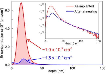
The annealing process is expected to promote an out-diffusion of the Er2+ ions from the Si-air interface, hence effectively reducing the final concentration of emission centers contained in Si. To establish the effective Er2+ concentration, we performed secondary ion mass spectrometry (SIMS) on a sample featuring the highest nominal implantation level (1 × 10¹⁴ions/cm2) before and after the annealing process, which is identical to the ones de-vised for the optical characterization. SIMS measurements were performed by using primary ions of O+2 at an acceleration energy of 3.0 kV with CAMECA IMS-7f. The detection area was 30 µm2 in diameter. The ion concentration level retrieved by SIMS before annealing matches perfectly the nominal values, confirming the excellent reliability of the implantation technique. On the other hand, as expected, the effective ion concentration after annealing drops to 1.5 × 1013 cm−2 (see Fig. 1). Therefore, to account for such an additional phe-nomenon, the nominal ion concentration has to be scaled by about a factor 7 in order to
Er concentration (x10 ions/cm ) 19 3 ~1.0 x 10 cm14 -2 ~1.5 x 10 cm13 -2
FIG. 1. SIMS depth profiles of a sample with nominal Er concentration of ≈ 1 × 1014 cm−2 before
and after annealing. The Er content is evaluated by integrating the concentration in the volume for the whole sample depth (see semi-transparent areas below the curves). The concentration measured after (marked blue) annealing is about 7 times lower than the one recorded before (marked red). Inset: depth profiles plotted in logarithmic scale.
attain the effective ion concentration in Si. A careful observation of Fig. 1 allows identifying a pile-up of the Er2+ ions close to the Si-air interface in the annealed sample, which we at-tribute to surface contamination. It is worth noting that the O+ amount is also reduced by about a factor 10, as can be derived by combining SRIM ion range simulations and diffusion equation, so the ratio around 1:1 is maintained. At these co-doping regimes, i.e. O:Er ≤ 2, density functional computations [25] indicates that the tetrahedral substitutional site is the most stable. In addition to that, according to Ref. [14], this is also the most optically active configuration due to a more favorable crystal field splitting in the case of the singly oxygen coordinated Er in a tetrahedral substitutional site instead of interstitial site.
We addressed Er ions implanted in Si and investigated their photoemission properties by means of a customized inverted confocal microscope coupled to a spectrometer (see Fig. 1b). In such an experimental arrangement, the light from a fiber-coupled laser diode at 792 nm wavelength, reflected by a cube beamsplitter (Thorlabs Inc.), is focused by a 0.85 NA objective (Nikon) to a diffraction-limited spot of about 1 µm in diameter at the sample plane. The emission from the Er2+ ions, collected through the same objective in epi-reflection geometry, is sent to a set of long-pass filters (1300 and 1350 nm cut-off wavelengths,
Piezo Laser LP filters BS z x y 0.85 N.A. Air SPAD Pelin-Broca Prism 50 mm 792 nm Er2+ Si SiO2 b)
Er /Si
2+Si
a) c) 20 mmEr /Si
2+Si
1.0 a.u. 0.7FIG. 2. a) Sketch of an implanted region, identified by gold trances for an easy identification. b) Experimental setup. BS: 70/30 beamsplitter, LP filters: two long-pass filters with 1300 and 1350 nm cut-off wavelengths, respectively; SPAD: InGasAs/InP single photon avalanche diode. Inset: side-view detail of the investigated sample showing the Er2+ implanted areas. c) Reflection map recorded at the excitation wavelength (792 nm).
Thorlabs Inc.) for rejecting the excitation reflected light. The filtered emission is then sent into a home-made spectrometer, which is composed simply by a rotating Pelin-Broca prism and a InP/InGaAs single photon avalanche diode (SPAD) and whose working principle is described in detail elsewhere [26]. Such an experimental setup allows recording fluorescence maps with a diffraction limited spatial resolution of about 1.2 µm together and emission spectra with a spectral resolution of about 10-15 nm. Figure 1c shows the reflectivity map recorded at the excitation wavelength on the corner of one of the pads, selected for the investigation to include also a non-implanted silicon region for control.
We collected PL maps on pads with effective Er+2 ions concentrations ranging from 1.5 × 1013 cm−2 down to 1.5 × 1011 cm−2 and exposed to two different O+ doses which ensure best emission performances. Emission maps collected on the corner of the square patches featuring higher ion implantation and higher oxygen dose are shown in Fig. 3a-d. The maps also reveal homogenous implantation of the ions in each pad, at least within the sensitivity of our optical technique. The maps sketched in Fig. 3 are obtained by averaging
20-30 subsequent maps with an integration time of 100 ms per pixel, resulting in a typical integration time of about 3 s per pixel. Each pixel in the maps returns the number of pho-tons recorded per second by the SPAD unit corrected by the dead-time of the detector. This procedure allows to account for the number of photons that, although reaching the sensing device, are lost due to the long dead-time of the detector (for details see Ref. [26]). By averaging the value of the signal in the patch and subsequently subtracting the background outside we have reconstructed the emission efficiency dependence on the concentration, as plotted in Fig. 3e. The emission, here plotted versus the effective concentration normalized according to the out-diffusion evaluated by SIMS measurements, shows a linear growth of the efficiency with increasing ion concentration that reaches saturation roughly above 0.5 × 10¹³ Er2+/cm2. Furthermore, both the linear and the logarithmic plots shows no significant difference between the two oxygen concentration, indicating that the annealing process op-timizes the Er2+/O+ ratio by forming the clusters. We have also acquired emission spectra of the samples by averaging onto different locations both inside and outside the implanted area (blue dots and black diamonds respectively in Fig. 3f). The spectrum acquired on the implanted region indicates the presence of a spectral feature around 1540 nm, which is typical of the erbium emission, together with a shoulder around 1400 nm. The background PL in the non-implanted area, which is visible between 1300 and 1700 nm, is attributed to residual photo-excited luminescence from the substrate.
As a proof of concept on the potential of our implantation technique we also realized micron-scale spots featuring the higher concentration of erbium. In particular, instead of removing the PMMA by EBL from the whole pad we have just removed a set of circular disks with variable diameter. Figure 4a shows the emission map collected on an area where we implanted a 3 × 3 array of 10 µm-diameter disks, placed at center-to-center distance of 20 µm (Er: 1 × 1014 cm−2 and O: 2.5 × 1013cm−2). Figure 4b shows the profile extracted by the central row in Fig. 4a (below) together with the profile extracted by a 5 × 5 array of of 5 µm-diameter disks located at a center-to-center distance of 10 µm (Er: 3 × 1013cm−2 and O: 2.5 × 1013 cm−2). Figure 4 highlights micrometer-sized isolated areas and it evidences also that the central disk features higher emission in both cases. This can be explained by the convolution between the mask and the shape of the ion implantation beam. It is also worth observing that, despite the low signal to ratio of these last measurements, the resolution appears to be mostly limited at this stage by the fabrication process rather than
300 150 Er PL (kcts/s) 2+ 20 mm ~1.5x10 ions/cm13 2 PL (kts/s) Er dose (10 cm )2+ 13 -2 a) b) c) d) Er PL (kcts/s) 2+ wavelength (nm) e) f) Non-implanted area Implanted area ~4.5x10 ions/cm12 2 ~1.5x10 ions/cm12 2 ~4.5x10 ions/cm11 2 120 80 40 0 0.0 0.5 1.0 1.5 PL (cts/s) O dose: ~ 2.5 x 10 ions/cm+ 12 2 O dose: ~ 1.0 x 10 ions/cm+ 13 2 1300 1400 1500 1600 1700 a b c d 0 5 10 15
FIG. 3. a)-d) Er Photoluminescence (PL) maps obtained at the same sample location as that of Fig. 1c by collecting the emission above 1350 nm at different Er2+ doses. The dashed lines indicate
implanted areas. e) PL emission intensity recorded by the SPAD. Dashed lines represent the linear fit at low implantation doses. Inset: Log-Log plot to highlight data at the low dose. Letters refer to panels a-d. f) Spectra recorded outside (black) and inside (blue) the implanted areas. A double Gaussian fit to the data (blue line) indicates two peaks centered at 1540 and 1400 nm, respectively.
117 121 125 129 Er PL (kcts/s) + 117 123 Er PL (kcts/s) + 20 mm a) 150 154 158 0 10 20 30 40 50 60 displacement ( m)m b)
FIG. 4. a) PL map of a 3 × 3 array of 10 µm-diameter disks with Er implantation (array pitch is 20 µm). Each disk is identified by a white dashed circle as a guide to the eye. b) Intensity profile of the mid row in the array (blue) and intensity profile extracted from a 5 × 5 array of 5 µm-diameter disks with a pitch of about 10 µm. The black arrows indicate the positions of the disk centers, confirming the 20 and 10 µm pitch, respectively. In both profile the central disks show higher intensity attributed to the shape of the ion beam size in our experiment.
by the optical system, which is about 1.3 µm [26].
We have evaluated the lower-bound number of ions that can be detected in these con-ditions by combining the estimation of the overall emitted photons by the implanted area from PL measurements, with given values of the Er emission cross-section and normalized thanks to the data from SIMS measurements. To extract the exact number of photons emit-ted by the centers embedded in the illuminaemit-ted area, we need to first estimate the amount of radiation directed in the semi-space of the collection optics. To do so, we have calcu-lated, by using finite-difference time-domain (FDTD) simulations, the emission pattern of a randomly-oriented dipole emitting at 1550 nm located inside Si, placed 10 nm underneath the Si/air interface. According to these calculations only 1 over 50 photons is emitted to-wards the collection objective. The objective collects about 90% of the light and transmits about 30% of it in this wavelength range. By accounting for (i) the throughput of the other collection optics (about 20%), (ii) the detector quantum yield (about 30%) and (iii) the light lost due to the overfilling of the detector area (about 15%) the overall throughput of the detection system can be estimated to be about 5 × 10⁻⁵. Under the hypothesis that all the implanted ions are active, the effective emitted photon flux for an ion concentration of
about 1.5 × 1012 cm−2, i.e. where the regime is still linear (see dot (c) in Fig. 3e), can be estimated to be about 4 × 10⁸ photons/s.
In addition, dividing the incident power at the ion plane (about 6 mW) by the excitation beam size at the focal plane (10−8 cm2, given a beam diameter of about 1.12 µm), one can easily obtain an excitation intensity of about 6 × 10⁵ W/cm2. As the emitted photon flux is equivalent to a power level of about 50 pW, the overall emission cross-section for the ions con-fined within the excitation volume can be estimated to be about 8 × 10⁻¹⁷cm2. By assuming a typical value for the emission cross-section of individual Er2+ of about 5 × 10⁻²²cm2 [27], we would calculate an effective number of excited ions at this nominal concentration that is about 105. This implies that, under the assumption that all the implanted Er atoms participate to the effect, in this study the minimum number of ions detected is about 104 for acquisition times that remains below 60 s. The lower-bound value for detectability is set in our measurements by two main limitations. On the one hand, the relatively high refractive index of the substrate guides the emitted light inside Si and away from the detection path, for a total loss of 95% of the photons. On the other hand, the detector noise and excessive deadtimes limits the signal-to-noise of our measurements.
By considering the overall estimated photon flux and the estimated number of photons one can calculate a photon flux per ion of about 4 × 10³ photons/s, corresponding to a PL lifetime in the millisecond range that is in line with values reported in literature. This implies a radiative lifetime for the ion in the silicon matrix of the order of the millisecond, which is very close to what reported in literature for this system.
To conclude, we demonstrated room temperature PL by low dose doping of ErOx centers implanted in natural Si at λ = 1.54 µm via the optical transition Er3+: 4I13/2 → 4I15/2. As the implantation depth is relatively close to the top surface, we demonstrate that - after taking into account the out-diffusion from the surface due to unavoidable annealing process - the number of centers is about one order of magnitude less. The signal to noise ratio of our system allowed detecting down to about 104 Er centers at room temperature. Our estimate is supported by the derived photon flux rate per individual ion, ≈ 4 × 10³ photons/s, which is close to the values reported in literature. The detection limit of our study is mainly set by the detector noise and the radiation losses in the silicon substrate. Hence, by engineering the substrate for effectively beaming the emitted light and employing a detector with higher performances the limit of few ion interrogation is within reach. These results set a step
forward towards the employment of ErOx centers in natural silicon optoelectronic devices for quantum networks at the telecomm wavelengths.
E.P. acknowledges JSPS, the Short Term Mobility Program 2015 of CNR and the Short Term Mobility Program 2016 of CNR. This work was supported by a Grant-in-Aid for Basic Research (B) (25289109) from MEXT and Young Scientists (A) (15H05413) from MEXT. The authors thank Maurizio Ferrari (CNR-IFN Trento), Giovanni Pellegrini (Politecnico di Milano) and Francesco Priolo (Universit di Catania)for useful discussions.
∗ [email protected] † [email protected]
[1] P. N. Favennec, H. L’Haridon, D. Moutonnet, M. Salvi, and M. Gauneau, Japanese Journal of Applied Physics 29, L524 (1990).
[2] D. J. Eaglesham, J. Michel, E. A. Fitzgerald, D. C. Jacobson, J. M. Poate, J. L. Benton, A. Polman, Y. Xie, and L. C. Kimerling, Applied Physics Letters 58, 2797 (1991).
[3] A. Polman, Journal of Applied Physics 82, 1 (1997).
[4] A. Polman, J. S. Custer, E. Snoeks, and G. N. van den Hoven, Applied Physics Letters 62, 507 (1993).
[5] R. Serna, M. Lohmeier, P. M. Zagwijn, E. Vlieg, and A. Polman, Applied Physics Letters 66, 1385 (1995).
[6] K. V. Feklistov, D. S. Abramkin, V. I. Obodnikov, and V. P. Popov, Technical Physics Letters 41, 788 (2015).
[7] E. Trave, G. Mattei, P. Mazzoldi, G. Pellegrini, C. Scian, C. Maurizio, and G. Battaglin, Applied physics letters 89, 151121 (2006).
[8] X. Zhang, T. Lin, P. Zhang, J. Xu, S. Lin, L. Xu, and K. Chen, Opt. Express 22, 369 (2014). [9] Y.-W. Lu, C. Huang, J.-G. Cheng, and A. N. Larsen, Journal of Alloys and Compounds 676,
428 (2016).
[10] H. Krzyanowska, Y. Fu, K. S. Ni, and P. M. Fauchet, ACS Photonics 3, 564 (2016). [11] Y. Wang, J.-m. An, Y.-d. Wu, and X.-w. Hu, Optoelectronics Letters 12, 47 (2016).
[12] J. Kalkman, A. Polman, T. Kippenberg, K. Vahala, and M. L. Brongersma, Nuclear Instru-ments and Methods in Physics Research Section B: Beam Interactions with Materials and
Atoms 242, 182 (2006).
[13] J. Kalkman, A. Tchebotareva, A. Polman, T. J. Kippenberg, B. Min, and K. J. Vahala, Jour-nal of Applied Physics 99, 083103 (2006), http://aip.scitation.org/doi/pdf/10.1063/1.2188050. [14] M. Louren¸co, M. Miloˇsevi´c, A. Gorin, R. Gwilliam, and K. Homewood, Scientific Reports 5
(2016).
[15] T. Shinada, S. Okamoto, T. Kobayashi, and I. Ohdomari, Nature 437, 1128 (2005).
[16] E. Prati, M. Hori, F. Guagliardo, G. Ferrari, and T. Shinada, Nature nanotechnology 7, 443 (2012).
[17] E. Prati, K. Kumagai, M. Hori, and T. Shinada, Scientific reports 6 (2016).
[18] E. Prati, Y. Chiba, M. Yano, K. Kumagai, M. Hori, G. Ferrari, T. Shinada, and T. Tanii, in 2015 Silicon Nanoelectronics Workshop (SNW) (IEEE, 2015) pp. 1–2.
[19] S. Tamura, G. Koike, A. Komatsubara, T. Teraji, S. Onoda, L. P. McGuinness, L. Rogers, B. Naydenov, E. Wu, L. Yan, F. Jelezko, T. Ohshima, J. Isoya, T. Shinada, and T. Tanii, Applied Physics Express 7, 115201 (2014).
[20] Y. Shimizu, H. Takamizawa, K. Inoue, F. Yano, Y. Nagai, L. Lamagna, G. Mazzeo, M. Perego, and E. Prati, Nanoscale 6, 706 (2014).
[21] C. Yin, M. Rancic, G. G. de Boo, N. Stavrias, J. C. McCallum, M. J. Sellars, and S. Rogge, Nature 497, 91 (2013).
[22] R. Kolesov, K. Xia, R. Reuter, R. St¨ohr, A. Zappe, J. Meijer, P. Hemmer, and J. Wrachtrup, Nature communications 3, 1029 (2012).
[23] J. Michel, J. Benton, R. Ferrante, D. Jacobson, D. Eaglesham, E. Fitzgerald, Y.-H. Xie, J. Poate, and L. Kimerling, Journal of applied physics 70, 2672 (1991).
[24] F. Priolo, G. Franzo, S. Coffa, A. Polman, S. Libertino, R. Barklie, and D. Carey, Journal of applied physics 78, 3874 (1995).
[25] A. Raffa and P. Ballone, Physical Review B 65, 121309 (2002).
[26] M. Celebrano, M. Baselli, M. Bollani, J. Frigerio, A. Bahgat Shehata, A. Della Fr-era, A. Tosi, A. Farina, F. Pezzoli, J. Osmond, X. Wu, B. Hecht, R. Sordan, D. Chrastina, G. Isella, L. Du, M. Finazzi, and P. Biagioni, ACS Photonics 2, 53 (2015), http://dx.doi.org/10.1021/ph500432k.
[27] T. J. Kippenberg, J. Kalkman, A. Polman, and K. J. Vahala, Physical Review A 74, 051802 (2006).