Charge transport modelling in organic semiconductors: From diodes to transistors,
memories and energy harvesters
Aldo Di Carlo and Francesco Santoni
Dept. of Electronics Engineering, University of Rome “Tor Vergata”, Rome, Italy Email: [email protected]
Introduction
Organic semiconductors are playing an increasingly important role for the fabrication of many electronic and optoelectronic devices such as organic light emitting diodes (OLEDs) [1], organic photovoltaics (OPVs) [2], organic thin-film transistors (OTFTs) [3] and organic memories [4]. Amorphous and/or regular assembly of polymers/small molecules can form such materials which typically exhibit complex electronic properties. Thus, a unified, comprehensive and transferable model of charge transport and injection in organic semiconductors is highly desired to help the understanding, development and optimization of organic devices. In this work, we will present the efforts made to identify a consistent scheme for charge transport in organic semiconductors and applications of this model to the description of diodes, resistive memories, OTFTs and OPVs.
The model
A conduction model should correctly account for (1) the energy structure of the organic material (2) the charge transport mechanism and (3) boundary conditions, such as the contacts. As for the electronic structure, weak bonds with negligible superposition of orbitals between molecules imply that electrons remain localized on their respective molecular sites, and their energy spectrum, taking into account polarization effects, is not very different from the one of the gas phase. Due to the molecular disorder and random orientation of molecular electric dipoles, energy levels are randomly distributed. Assuming there is no correlation between adjacent sites, the energy distribution (i.e. the density of states – DOS) has a gaussian profile. This model is commonly referred to as gaussian disorder model, GDM [10]
Charge transport in organic semiconductor can be described at semi-classical level by using drift-diffusion (DD) equations [6] with a suitable mobility model [7-8] derived from a Miller-Abrahams phonon assisted hopping model [9-11].
When modeling organic devices, charge injection is one of the critical issues, since current in these devices is essentially injection controlled. Estimation of device parameters, such as field-effect mobility, depends critically on the barrier height [14]. Varying the metal/organic semiconductor barrier height by 0.3 eV a variation of one order of magnitude can be found in the extracted mobility. According to the standard Schottky-Mott model, the potential
rise at metal/semiconductor interface is equivalent to the difference of their respective work functions. However, the presence of localized states inside the band gap can alter this picture significantly. According to the IDIS (Induced Density of Interface States) model [6-8], at the contact/organic interface the continuum of metal states overlaps with the organic semiconductor states; as a result the HOMO and LUMO levels broaden, producing a tail of interface states deep inside the band gap. Once experimental injection barriers are known, IDIS model can be used to estimate a realistic density of interface states to be used in the simulation. In the following, we will present some simulation results of organic and hybrid organic/inorganic devices focusing of the influence of the charge injections at the contacts and on the influence of localized traps at the interfaces.
Charge injection at the contacts
Experimental and simulation results for electron injection barriers in Alq3 and -NPD are plotted in Fig. 1. The IDIS
model, although being a clear approximation, works quite well to get a first estimate of simulation parameters, which can successively fine-tuned to set the density of traps and consequently the injection barrier.
3.6 4.0 4.4 4.8 0.0 0.5 1.0 1.5 2.0 -NDP Ele ctron I nj ectio n Barri er [ eV]
Contact Work Function [eV] Experimental Data
Simulation
Alq3
2.4 3.2 4.0 4.8 5.6
Figure 1: Experimental data and simulation results obtained with the IDIS model for electron injection barriers in Alq3 and -NPD
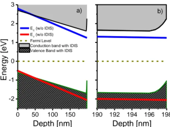
The use of a proper description of the contact permits to define an injection model consistent with the properties of the organic semiconductor. This is reported in Fig. 2 where the experimental I-V characteristics [15] of a ITO/-NPD/Pd diode are compared with simulations performed with different injection contact models. Mobility used for Fig. 2 are reported in Fig. 3 together with experimental data [16]. When simulations are performed with the Pd workfunction as a fitting parameter and without the use of IDIS, the fit of I-V
characteristics produce unrealistic low mobility values (Fig. 3), while if the experimental mobility is used, the simulated I-V curve do not fit with the experiment (Fig. 2.a). On the opposite, if we use the nominal workfunction of Pd (5 eV) and apply the IDIS model to get the correct barrier shift, we are able to reasonably fit both I-V characteristics and mobility data (Fig. 2.b). The effect of interface states near the contact region is shown in Fig. 4. The band bending near the Pd contact explains the variation of the built-in potential in the device without the need to use an effective Pd work function.
1 2 3 4 5 1E-10 1E-9 1E-8 1E-7 1E-6 1E-5 1E-4 1E-3 0.01 1 2 3 4 5 b) Exp. Data Mensfoort et al. [15] Naka mobility [16] Exp. Data Cu rren t De nsi ty [A /cm 2 ] Applied Voltage [V] Mobility tuning Mobility tun. + IDIS
a)
Applied Voltage [V] Figure 2: Experimental and simulated IV characteristics of the ITO/-NPD (200 nm)/Pd device reported in Ref. [15]. Simulated curves are obtained a) using data from [15] and [16] and b) by fitting the mobility ad I-V with and without IDIS model.
200 300 400 500 1E-5 1E-4 1E-3 0.01 Hole m obil ity [cm 2 /Vs] (Electric Field)1/2 [V1/2/cm1/2]
Exp. Data (Naka et al.) Mobility from Mensfoort et al. fitting Fitted mobility (Naka et al,) Mobility extracted with IDIS
Figure 3: Experimental and simulated -NPD hole mobility. Simulations mobility data are related to the IV simulation of Fig. 2.
The transferability of the model has been verified by simulating I-V characteristics of several organic devices (Fig. 5). In particular we simulated a bi-layer device (ITO/ -NPD/Alq3/Al), i. e. a typical OLED structure, showing the
applicability of our model in the analyses and optimization of real devices of industrial interest.
Tunneling from contact metal into localized/semi-localized states in the organic semiconductor play an important role in the low bias region. Due to the presence of a built-in potential (Fig. 4b), the drift-diffusion model cannot explain the low bias current observed experimentally. This is clearly shown in Figs. 2 and 5 where below 1-2 V the simulated current and the experimental one differ considerably.
0 50 100 150 -2 -1 0 1 2 3 190 192 194 196 198 b) Ene rgy [ eV] Depth [nm] E C (w/o IDIS) EV (w/o IDIS) Fermi Level Conduction band with IDIS Valence Band with IDIS
a)
Depth [nm]
Figure 4: a) Band profile of the ITO/-NPD/Pd device using Mensfoort et al. [15] parameters without IDIS and our simulation with IDIS. To obtain the correct built-in potential, Mensfoort et al. used an effective work function for Pd; we used instead the actual Pd work function; the effective built-in potential is due to states inducing band bending close to contact interface as magnified in b) 1E-9 1E-7 1E-5 0 2 4 6 8 10 12 1E-8 1E-6 1E-4 0.01 Exp. Data Simulation ITO/Alq3(100 nm)/Al Cu rren t De nsi ty [A /cm 2 ] Applied Voltage [V] ITO/-NDP(60nm)/Alq3(80nm)/Al
Figure 5: (top) Experimental [20] and simulated IV characteristics of a ITO/Alq3 (100 nm)/Al device. (bottom) Experimental [21] and simulated IV characteristics of ITO/-NPD (60 nm)/Alq3 (80 nm)/Al device.
To account for tunneling, the semi-classical DD model can be coupled in a multiscale fashion [5] with quantum approaches such as the Non Equilibrium Green Functions (NEGF) method [18]. DD-NEGF have been used to simulate the low bias current due electron injection into gap states near the cathode in a PEDOT:PSS/Alq3 (150nm)/Ag device (Figs.
6). Electrons are injected into gap states before the applied bias reaches the built-in potential, thus explaining the low-bias current.
This multiscale approach has been also applied to clarify the relevance of tunneling in organic non-volatile resistive memories based on conductive filaments [19] (Fig. 7, 8). It has been proposed [22-23] that tunneling in disconnected filaments could result in an appreciable and variable change of the current in the higher resistance states. We investigated this mechanism with the NEGF method, calculating the tunneling current in disconnected filament tips near the anode (Fig. 7). Since quantum calculation are computationally very expensive, they are performed only in a small region around the tip (indicated in the same Fig. 7), while in the main
volume of the device a faster semiclassical drift-diffusion model is still employed. The two models can be coupled self-consistently as follows: 1) The semiclassical Poisson + drift-diffusion model is solved across the whole device; 2) The potentials calculated in the previous step are used to calculate the tunneling current with the NEGF method; 3) From the current calculated in step 2 an average effective conductivity is calculated and then used in the drift-diffusion; 4) the Poisson + drift-diffusion system is solved; 5) The whole procedure is repeated iteratively till the solution converges.
This procedure is applied to the system depicted in Fig. 7 for two different typical tunneling gaps (1nm and 2 nm, approximately the size of an Alq3 molecule). The results of our
simulations (Fig. 8) strongly suggest that the tunneling effect, even if present, is negligible for the global behavior of this device and that the total current can be accounted for by fully formed and connected filaments whose conduction can be described in a semi-classical drift-diffusion fashion.
0 1 2 3 4 1E-10 1E-9 1E-8 1E-7 1E-6 Cu rren t De nsi ty [A /cm 2 ] Applied Voltage [V] Experimenta data NEGF + DD DD
Figure 6: Experimental and simulated I-V characteristics of PEDOT:PSS/Alq3 (150nm)/Ag. Gap states near the Ag electrode are responsible for the low-bias behavior of the current. Tunneling trough these states have been calculated by using NEGF+DD.
Figure 7: The mesh used to calculate the tunneling current between the tip of a not-connected filament and the anode. The quantum region is indicated. Outside that region the semi-classical Poisson + DD model is used. The two regions are coupled self-consistently.
Trap states at the interfaces
Interfaces in organic devices are very common and often used to achieve the final functionality of the device itself. Interfaces arises when two or more organic semiconductors
are used or mixed with inorganic materials or when different crystal domains forms. To describe the charge transport in these systems, traps formed at the interfaces cannot be neglected. 0 1 2 3 4 5 1E-17 1E-14 1E-11 1E-8 1E-5 0.01 10 Exp. Data Exp. Data NEGF with 1 nm gap NEGF with 2 nm gap
Cu rren t De nsi ty [A /cm 2 ] Applied Potential [V]
Figure 8: Comparison between experimental data of some resistive states measured in organic memories based on filament forming [19] (shaded area) and simulation results of tunneling conduction calculated with NEGF. This results rule out tunneling as an important mechanism in the resistive memory devices under investigation.
Transport in OTFT, for example, is ruled by the presence of grain boundaries between regular/crystalline phases of the organic semiconductor [24]. Grain boundaries can be model by considering a single trap level with a given concentration and energy. Due to the potential barrier induced by the trap level, the field-effect-extracted mobility is not linearly related to the grain size, but presents a rather abrupt reduction for a grain size smaller than 2 m. (Fig 9)
Figure 9: Comparison between experimental data and simulation results of Pentacene OFET mobility as a function of grain size. (inset) AFM of Pentacene grains with different sizes.
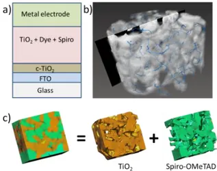
Interface traps play a key role in hybrid organic/inorganic devices such as the solid-state Dye Solar Cells (ss-DSC), a system that outperform other light harvesters in indoor lightening. Multiscale simulation of ss-DSC have been
performed by considering the real morphology of the mesoporous TiO2 and the Spiro-OMeTAD as obtained by
TEM tomography (Fig. 10).
Fig. 10 a) Layer sequence of the ss-DSC. b) TEM Tomography (G. Divitini and C. Ducati, Cambridge University, UK) of the ss-DSC active layer, c) Mapping of the TEM tomography on the simulation grid. The TiO2 and Spiro-OMeTAD domains are well identified and considered as specific regions in the simulations.
The extracted TEM morphology has a linear dimension of few nanometers while the entire device is of micron size. In these cases, a multiscale approach is well suited: in the simulation, the real morphology region is embedded in an effective medium where TiO2 and Spiro-OMeTAD properties
are averaged (Fig. 11) [25]. This also permit to apply correct boundary conditions to the simulated device. Special attention should be made in the definition of recombination rate when passing from the effective medium to the real morphology region. In fact, recombination rate should be consistent between the two regions otherwise spurious effect can show-up [25].
Fig. 11 Multiscale approach concept for the simulation of ss-DSC. The real morphology region, obtained from TEM tomography, is embedded in an effective material accounting for TiO2 and Spiro-OMeTAD in an average way.
The use of a real morphology region allows us to accurately describe the electrostatics between electrons, holes and charged trap states at the TiO2/Spiro interface. Simulation
results show that electrons trapped at the TiO2 surface states
induce a high density of holes at the TiO2/Spiro interface and
consequently a screening of the long-range electric field and an increased e-h recombinations (Fig.12). This clarify the role of ionic additives, such has LiTFSI which are used for the fabrication of solid-state DSC: these ions screen the trapped electrons reducing hole accumulation. As shown in Fig. 12b, when interface charged traps are screened by ions, the current flows far from the interfaces, reducing the recombination and increasing the total current. Short circuit current is doubled when ions are screened.
Fig. 12 Hole current density/flow in the ss-DSC. a) Trapped electrons at the TiO2 surface induce a hole current flux close to the TiO2/Spiro interface enhancing recombination. b) By adding ionic additives (LiTFSI) the trapped charge is screened by the ions and holes can flow far from the interface reducing the recombination.
Acknowledgments:
We acknowledge the support of EU-H2020 project “MOSTOPHOS” (n. 646259)
References:
[1] C. Murawski, K. Leo, M. C. Gather, Advanced Materials 25, (2013), 6801-6827; P. Kathirgamanathan et al. IEEE/OSA Journal of Display Technology 11, (2015), 480.
[2] H. Youn , H. J. Park , L. Jay Guo Small 11, (2015), 2228; T. M. Brown, A. Reale, A. Di Carlo, in Thin Film Solar Cells: Current Status and Future
Trends, Nova Science Publishers, (2012), 245.
[3] H. Sirringhaus, Advanced Materials 26, (2014), 1319; S. Mandal and Y.-Y. Noh, Semicond. Sci. Technol. 30 (2015) 064003.
[4] T. Lee, and Y. Chen, MRS Bulletin, Volume 37, Issue 2, February 2012, Pages 144.
[5] M. Auf der Maur, et. al, IEEE TED 58, (2011), 1425. [6]F. Santoni et al., Org. Electron. 15 (2014) 1557. [7] J. Cottar, P. A. Bobbert, Phys. Rev. B 74 (2006) 115204 . [8]W. F. Pasveer et al., Phys. Rev. Lett. 94 (2005) 206601. [9] A. Miller, E. Abrahams, Phys. Rev. 120 (1960) 745. [10]] H. Bässler, Phys. Stat. Sol. (b) 175 (1993) 15. [11] N. Tessler et al., Adv. Mater. 21 (2009) 2741. [12] A.M. Cowley, S.M. Sze, J. Appl. Phys. 36 (1965) 3212. [13] H. Vazquez et al., Appl. Surf. Sci. 234 (2004) 107.
[14] A. Bolognesi, A. Di Carlo, P. Lugli, App. Phys. Lett. 81 (2002) 4646. [15] S. L. M. van Mensfoort et al., J. Appl. Phys. 107 (2010) 113710. [16] S. Naka et al., Synth. Met. 111–112 (2000) 331.
[17] P. Cosseddu et al., Org. Electron. 15 (2014) 3595. [18] A. Pecchia, A. Di Carlo, Rep. Prog. Phys. 67 (2004) 1497.
[19] S. Nau et al., Adv. Mater. 26 (2014) 2508; F. Santoni et al. IEEE Trans. Nanotechnol. (to be published)
[20] S.H. Kim et al., ETRI J. 26 (2004) 161. [21] E. Tutis et al., J. Appl. Phys. 93 (2003) 4594.
[22] H. -S. P. Wong et al., Proceedings of the IEEE 100 (2012) 1951. [23] S. Yu et al., in IEDM Tech. Dig. (2011) 17.3.1.
[24] A. Di Carlo et al., Appl. Phys. Lett. 85 (2005) 263501. [25] A. Gagliardi et al. Nanoscale,(2015) 7, 1136.

![Figure 8: Comparison between experimental data of some resistive states measured in organic memories based on filament forming [19] (shaded area) and simulation results of tunneling conduction calculated with NEGF](https://thumb-eu.123doks.com/thumbv2/123dokorg/7597859.114042/3.918.502.807.708.928/comparison-experimental-resistive-filament-simulation-tunneling-conduction-calculated.webp)