Production and Characterization of
ZnO/Graphene Devices for Energy
Harvesting
Faculty of Civil and Industrial Engineering
Ph.D School on Electrical, Materials and Nanotechnology
Engineering
Ph.D in Nanotechnology Engineering
ING-IND/31- Electrotechnics
XXXI Cycle 2015-2018
Ph.d Candidate
Marco Fortunato
1201930
Supervisor
Professor Maria Sabrina Sarto
If we knew what it was we were doing, it would not be called
research, would it?
A. Einstein
v
Contents
Abstract ... 1 Chapter I Introduction ... 5 1.1 Piezoelectric Effect ... 8 1.2 Piezoelectric Materials ... 13 1.3 Piezoelectric Devices ... 171.4 Thesis Objective and Organization ... 19
Chapter II Scanning Probe Microscopy ... 23
2.1 Atomic Force Microscopy ... 23
2.1.1 Contact Mode ... 25
2.1.2 Tapping Mode ... 28
2.2 Piezoresponse Force Microscopy (PFM) ... 30
2.2.1 History of PFM ... 30
2.2.2 Operating Principle of PFM ... 31
2.2.3 Imaging of the Piezoelectric Domains ... 33
2.2.4 Quantification of the Piezoelectric Coefficient ... 34
Chapter III Zinc Oxide Nanostructures ... 41
3.1 Introduction ... 41
3.2 Growth of ZnO Nanorods ... 41
3.3 Techniques used for the characterization of ZnO Nanostuctures .. 43
3.3.1 Morphological and Chemical Characterizations ... 45
3.3.2 Structural Analysis ... 47
3.3.3 Chemical Composition ... 47
3.3.4 Photoluminescence Properties ... 49
3.3.5 Piezoelectric Properties... 51
3.4 Growth of ZnO Nanowalls ... 53
3.4.1 Morphological and Chemical Characterizations ... 53
3.4.2 Structural Analysis ... 54
3.4.3 Chemical Composition ... 56
3.4.4 Photoluminescence Properties ... 57
3.4.5 Piezoelectric Properties... 59
vi
4.1 Introduction ... 63
4.2 Deposition of PVDF Nanocomposites ... 64
4.2.1 Route 1 (R1) – Direct exfoliation of expanded graphite in PVDF solution ... 65
4.2.2 Route 2 (R2) – Solution-induced incorporation of nanofiller in PVDF . 67 4.2.3 Route 3 (R3) – Dissolution of hexahydrate salt of different metals (HMS) in PVDF ... 68
4.2.4 Route 4 (R4) – Combined nanofiller dispersion and HS- dissolution ... 69
4.3 Techniques used to characterize the PVDF Nanocomposites ... 69
4.3.1 Morphological Characterization ... 71
4.3.2 FT-IR Analysis ... 75
4.3.3 XRD Analysis ... 77
4.3.4 Piezoelectric properties ... 79
Chapter V Energy Harvesting Device ... 90
5.1 Introduction ... 90
5.2 Device Fabrication ... 92
5.2.1 Deposition of PVDF Films ... 92
5.2.2 Deposition of Graphene-Gold Electrodes ... 92
5.3 Morphological Characterizations ... 93
5.4 Electrical properties ... 94
5.5 Piezoelectric response ... 95
Chapter VI Conclusions and Future Perspective ... 100
Bibliography ... 106
Acknowledgments ... 115
1
Abstract
In this thesis, different types of innovative highly performing piezoelectric nanomaterials and nanocomposites have been synthesized and characterized for energy harvesting application. In order to evaluate the piezoelectric properties of the produced materials, a novel approach to quantitatively evaluate the effective piezoelectric coefficient 𝑑𝑑33,
trough Piezoresponse Force Microscopy (PFM), has been developed. PFM is one of the most widely used techniques for the characterization of piezoelectric materials at nanoscale, since it enables the measurement of the piezo-displacement with picometer resolution. PFM is a non-invasive and easy to use test method; it requires only a bottom electrode (no need of a top-electrode deposition over the material under test), thus considerably simplifying the test structure preparation. In particular, in order to have a quantitative information on the 𝑑𝑑33 a calibration protocol
was developed. To get a macroscale characterization of the piezoelectric coefficient, the PFM signal is averaged over different areas of the sample. The proposed method allows to precisely evaluate the piezoelectric coefficient enabling a proper comparison among the different materials analysed.
Two different classes of piezoelectric materials have been synthesized and characterized:
• zinc oxide nanostructures, in particular zinc oxide nanorods (ZnO-NRs) and zinc oxide nanowalls (ZnO-NWs),
• polyvinylidene fluoride (PVDF) nanocomposites films.
The produced piezoelectric materials were fabricated using process which are cost-effective, time-consuming and easy to scale-up. The ZnO nanostuctures were grown by chemical bath deposition (CBD), that guarantees high deposition rate on a wide variety of substrates. PVDF nanocomposite films were produced with a simple solution casting method, without the need of subsequent electrical poling step. To enhance the piezoelectric properties of PVDF films we investigated different PVDF nanocomposite films:
2
- PVDF filled with Graphene nanoplatelets (GNPs) or with ZnO-NRs; - PVDF filled with different types of hexahydrate metal-salts (HMS); - PVDF filled with HMS in combination with nanofillers, like GNPs
or ZnO-NRs.
We found that the piezoelectric coefficient of the ZnO-NRs is (7.01±0.33) pm/V and (2.63±0.49) pm/V for ZnO-NWs. The higher piezoelectric response of ZnO-NRs is believed to be due to a better crystallinity and a less defectiveness of the ZnO-NRs if compared to the ZnO-NWs, as it has been confirmed by X-ray diffraction (XRD) spectra and by photoluminescence spectroscopy (PL) measurements.
The neat PVDF show a d33 limited to 4.65 pm/V; when the nanofillers
are added the d33 increases up to 6 pm/V. This value reaches 8.8 pm/V
when a specific hexahydrate metal-salts: [Mg(NO3)2∙6H2O] is dispersed in
the PVDF polymer matrix.
From the comparative analysis of the synthesized materials we found that the sample produced using the dissolution of HMS in PVDF shows the best piezoelectric response (8.8 pm/V) and the most attractive structural and mechanical properties to fabricate a flexible nanogenerators. Therefore, a porous piezoelectric HMS-PVDF nanocomposite film has been used as active material to fabricate flexible nanogenerator. To build such a device, graphene-gold flexible top electrodes were developed. The bilayer electrode structure avoids short circuits between top and bottom electrodes, observed in the absence of graphene interlayer. The nanogenerator was tested using a commercial mini-shaker and operated successfully. The piezoelectric coefficient determined from the electromechanical tests was 9.00 pm/V, which is in good agreement with the one (8.88±3.14) pm/V measured through PFM on the same PVDF film without top electrode. We also measured the piezoelectric coefficient of PVDF using PFM with and without top electrode and both values were found to be in close agreement. This finding suggests that the local characterization using PFM is also a good representation of the global piezoelectric properties of the samples.
3
The progress on advanced piezoelectric materials reported in this work opens new opportunities to fabricate energy harvesters and sensors for wearable and smart clothing applications.
4
C
HAPTER
I
I
NTRODUCTION
1.1 PIEZOELECTRIC EFFECT 1.2 PIEZOELECTRIC MATERIALS 1.3 PIEZOELECTRIC DEVICES5
Chapter I
Introduction
All materials can be categorized according to their electrical conductivity into: conductors, semiconductors, and insulators. Where in conductors and semiconductors, electrons are free to move (in semiconductors under certain condition) an insulator has only bound electrons. Since the electrons cannot move in insulators, when an electric field is applied, they can only be displaced within the unit cell i.e. the can be polarized, causing dielectric polarization. If the dielectric is composed of regions of atoms with homogenous polarization (domains), the applied field not only polarizes those atoms, but also can reorient the domains, so that their symmetry axes align to the field (see Fig. 1).
Fig. 1 Piezoelectric domains in a ceramic (a) before, (b) during and (c) after the application of an external electric field.
Generally, the polarization varies approximately linearly with the electric field. Another qualification of physical solids can be made on basis of their crystallinity. When atoms or molecules are packed in a regularly ordered repeating pattern, materials are called crystalline. Materials are called single crystal when the crystal lattice of the entire sample is continuous, with no grain boundaries [1]. Several special electrical phenomena can occur in dielectric crystalline materials. Among these of relevance are:
• Piezoelectricity means “pressure electricity”, from the Greek verb πιέζειν (pi𝑒𝑒́zein), which means squeeze or press. It is the phenomenon of some materials of generating an electrical potential in response to an applied stress;
6
• Pyroelectricity, the phenomenon of some materials of generating an electrical potential when they are heated or cooled;
• Ferroelectricity, the phenomenon of some materials where the spontaneous polarization can be reversed by applying an electric field.
Ferroelectric materials are a sub-group of piezoelectric materials (i.e. all ferroelectrics are piezoelectrics but not all piezoelectrics are ferroelectrics) which are a part of the largest category of dielectric materials. Therefore, piezoelectric materials combine properties of ferroelectric and dielectric materials with the further characteristic of varying their polarization due to an external deformation and vice versa.
In this thesis we will focus on the study of some piezoelectric materials. Piezoelectricity is the property of many materials to develop a polarization (or dielectric displacement) when a mechanical stress is applied (the materials is squeezed or stretched), as sketched in Fig. 2 (a). This phenomenon is called direct piezoelectric effect and the sign of the polarization is reversed according to whether the deformation is due to a compression or a pull. Vice versa, a strain is developed when an electric field is applied, Fig. 2 (b). and in this case the phenomenon is called converse piezoelectric effect.
Fig. 2 Direct piezoelectric effect (a) and converse piezoelectric effect (b).
P��⃗
7
Whether a material is piezoelectric depends on its microscopic charge distribution. For example, the charge distribution in Fig. 3 (a), when deformed into Fig. 3 (b), results in a net polarization [2].
Fig. 3 Origin of the direct piezoelectric effect [2].
The first experimental demonstration of the connection between the macroscopic piezoelectric phenomena and the crystallographic structure was published in the 1880 by Pierre and Jacques Curie, who measured the surface charging that appeared on appropriately prepared crystals (i.e. tourmaline, quartz, and salt of Rochelle) subjected to mechanical stress [3]. The first application of piezoelectricity was developed by Langevin, during the first world war, who built the first sonar (an underwater ultrasound source) made by piezoelectric quartz elements interposed between steel plates. The sonar success stimulated the development of other devices exploiting the piezoelectric effect. The crystal frequency control became essential for the broadcasting industry and radio communication. Most of classical piezo applications (microphones, accelerometers, ultrasonic transducers, bending element actuators, phonograph pick-ups, filters of signal, etc.) were developed despite the fact, that the available materials often limited the performance of the devices. During the second world war, the discovery of the possibility to induce the piezoelectricity applying a strong electric field to metal oxides, synthesized in order to align the dipole domains, allowed new piezo-electric applications and opened the way to intense research on piezoceramics. However, it required a long time and the discovery of new materials before piezoelectric devices became competitor to the
electro-8
dynamic and magnetic based devices, which for a long time were the only way to transform electrical energy or signals into mechanical ones or vice versa effectively. Nowadays the principal research lines on piezoelectric materials are:
• piezoelectric ceramics based on barium titanite and on zirconate titanate lead (PZT).
• crystals and nano-crystals with a perovskite structure
• piezoelectric polymers like Poly[vinylidene fluoride] (PVDF) and its co-polymer poly[vinylidenefluoride-co-trifluoroethylene] (PVDF-TrFE).
The coupling of electrical and mechanical energy makes the piezoelectric materials useful for a wide range of applications, grouped into the following classes:
• Sensors - they take advantage of the direct effect. • Actuators - they take advantage of the converse effect.
• Energy conversion – convert mechanical energy into electricity or vice versa.
1.1 Piezoelectric Effect
A material can only be piezoelectric if its crystalline structure does not have a symmetry centre or as said is non-centrosymmetric. Among the 32 crystallographic groups 21 are non-centrosymmetric and of these 20 are piezoelectric. A stress (traction or compression) applied to this type of material modifies the position between the sites containing the positive and negative charge in each elementary cell, leading to a net polarization on two opposite surfaces of the crystal. The relationship between the applied stress σ and the resulting polarization P is linear:
𝑃𝑃 = 𝑑𝑑direct∙ 𝜎𝜎 (1.1)
in which 𝑑𝑑direct is the piezoelectric coefficient. This means that the
induced polarization varies proportionally with the applied stress and is also dependent on the direction; according to this principle, compressive or tensile stress generates electric fields, and therefore a voltage. In the case of a compressive stress the output voltage has the same polarity of
9
the crystal domains, while if we apply a tensile stress the output voltage has the opposite polarity of the crystal domains. As already mentioned, the phenomenon is also reciprocal, so the same material, if instead of being subjected to a force it is exposed to an electric field, it will undergo an elastic deformation or strain ε, which causes, to a first approximation, an increase or a reduction of its dimension along the direction of the applied electric field, according to the polarity of the applied field (Fig. 2 (a), (b)):
𝜀𝜀 = 𝑑𝑑converse∙ 𝐸𝐸 (1.2)
The piezoelectric constant 𝑑𝑑direct is conventionally expressed in
Coulomb per Newton [C/N] for the converse piezoelectric coefficient 𝑑𝑑converse as meter per Volt [m/V]. The coefficient connecting the field and
the strain in the converse effect is the same as that connecting the stress and the polarization (𝑑𝑑direct= 𝑑𝑑converse). The proof of this equality is
based on thermodynamic reasoning. More precisely the constitutive relations for a piezoelectric material can be expressed as [4]:
𝐷𝐷𝑖𝑖 = 𝑒𝑒𝑖𝑖𝑖𝑖𝜎𝜎𝐸𝐸𝑖𝑖+ 𝑑𝑑𝑖𝑖𝑖𝑖𝑑𝑑 𝜎𝜎𝑖𝑖𝑗𝑗 (1.3)
𝜀𝜀𝑗𝑗 = 𝑑𝑑𝑖𝑖𝑗𝑗𝑐𝑐 𝐸𝐸𝑖𝑖+ 𝑠𝑠𝑗𝑗𝑖𝑖𝐸𝐸 𝜎𝜎𝑖𝑖 (1.4)
which can be written as:
�𝐷𝐷𝜀𝜀 � = �𝑒𝑒𝑑𝑑𝜎𝜎𝑐𝑐 𝑑𝑑𝑠𝑠𝐸𝐸𝑑𝑑� �𝐸𝐸𝜎𝜎� (1.5) where vector D of size (3×1) is the electric displacement (C/m2), ε is the
strain vector (6×1) (dimensionless), E is the applied electric field vector (3×1) (V/m) and σm is the stress vector (6×1) (N/m2). The piezoelectric
constants are the dielectric permittivity 𝑒𝑒𝑖𝑖𝑖𝑖𝜎𝜎 of size (3×3) (F/m), the
piezoelectric coefficients 𝑑𝑑𝑖𝑖𝑖𝑖𝑑𝑑 (3×6) and 𝑑𝑑𝑖𝑖𝑗𝑗𝑐𝑐 (6×3) (C/N or m/V), and the
elastic compliance 𝑠𝑠𝑗𝑗𝑖𝑖𝐸𝐸 of size (6×6) (m2/N). The piezoelectric coefficient
𝑑𝑑𝑖𝑖𝑗𝑗𝑐𝑐 (m/V) defines strain per unit field at constant stress and 𝑑𝑑𝑖𝑖𝑖𝑖𝑑𝑑 (C/N)
defines electric displacement per unit stress at constant electric field. The superscripts c and d have been added to differentiate between the converse and direct piezoelectric effects, though in practice, these coefficients are numerically equal. The superscripts σ and E indicate that the quantity is measured at constant stress and constant electric field respectively. To improve the piezoelectric properties, generally a “poling” process is performed, i.e. a high electric field (1--4MV/cm) is applied to
10
the material to align most of the unit cells as closely parallel to the applied field as possible. Usually, the poling process is carried out at temperatures higher than the room temperature (typically in the range of 60°C--100°C) to be more effective. This process imparts a permanent net polarization to the piezoelectric materials, although not all the dipoles are oriented along the direction of the field, due to the anisotropy that characterizes these materials. To realize the poling process electrodes must be deposited onto the piezoelectric material. The poling procedure is sketched in Fig. 4.
Fig. 4 Poling procedure: random orientation of polar domains prior to polarization (a); polarization in DC electric field (b); remanent polarization
after the electric field is removed (c).
The direction of the applied field is usually along the thickness and is denoted as the 3- axis and the 1-axis and 2-axis are in the plane of the sheet. The piezoelectric materials are anisotropic materials. For that reason, is necessary to use a notation that allows to identify the directions in which mechanical stresses and electric responses occur and vice versa. The directions X, Y, Z are for convenience of notation indicated respectively with the number 1, 2 and 3, while the rotation around these axes are indicated by numbers 4, 5 and 6, as showed in Fig. 5.
11
The 𝑑𝑑𝑖𝑖𝑗𝑗𝑐𝑐 matrix can then be expressed as:𝑑𝑑 = 31 32 33 24 15 0 0 0 0 0 0 0 0 0 0 0 0 0 d d d d d (1.6)
where the coefficients d31, d32 and d33 relate to the normal strain in the 1, 2
and 3 directions respectively to a field along the poling direction, E3. The
coefficients d15 and d24 relate the shear strain in the 1-3 plane to the field E1
and shear strain in the 2-3 plane to the E2 field, respectively. Note that it
is not possible to obtain shear in the 1-2 plane purely by application of an electric field.
Generally, the compliance, the permittivity metrics and the stress vector are of the form:
𝑠𝑠𝐸𝐸= 11 12 13 12 22 23 13 23 33 44 55 66 0 0 0 0 0 0 0 0 0 0 0 0 0 0 0 0 0 0 0 0 0 0 0 0 s s s s s s s s s s s s (1.7) 𝑒𝑒𝜎𝜎= �𝑒𝑒11 𝜎𝜎 0 0 0 𝑒𝑒22𝜎𝜎 0 0 0 𝑒𝑒33𝜎𝜎 � (1.8) 𝜎𝜎 = 1 2 3 4 5 6
σ
σ
σ
σ
σ
σ
= 11 22 33 23 31 12σ
σ
σ
σ
σ
σ
(1.9)Equation (1.3) is the formula that describes the direct piezoelectric effect and that is the so called “sensor equation”. The piezoelectric material is exposed to a stress field and generates a charge in response. Equation (1.4) is the formula that describes the converse piezoelectric effect and that is the so called “actuator equation”. The actuator is bonded
12
to a structure and an external electric field is applied to it, which results in an induced strain field. In the case of a piezoelectric material, where the applied external electric field is zero, Equation (1.5) becomes:
�𝐷𝐷𝐷𝐷12 𝐷𝐷3 � = 1 2 15 3 24 4 31 32 33 5 6 0 0 0 0 0 0 0 0 0 0 0 0 0 d d d d d
σ
σ
σ
σ
σ
σ
(1.10)This equation summarizes the principle of operation of piezoelectric materials. A stress field causes surface charging to be generated (Equation 1.10) as a result of the direct piezoelectric effect. Note that shear stress in the 1-2 plane, 𝜎𝜎6, is not capable of generating any electric response. If we
considered a parallelepiped of a piezoelectric material and two electrodes placed on its faces, there are 3 possible types of energy conversion:
• Effect 33 → the stress is applied along the direction 3 (transverse stress) and the voltage is in direction 3: this is the effect that will studied in this thesis.
• Effect 31 → the stress is applied along the direction 1 (longitudinal stress) and the electric field is again in direction 3;
• Effect 15 → the stress is applied along the direction 5 (shear stress) and the tension is in direction 1.
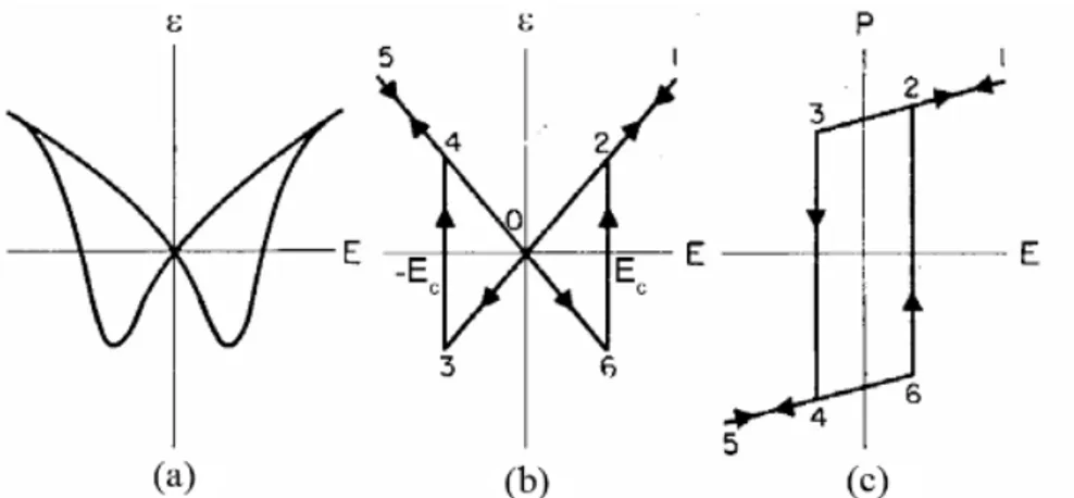
Fig. 6 Relation stress-voltage [5].
The behaviour of strain versus applied electric field appears in the shape of a butterfly loop (Fig. 7 (a)). In an ideal case (Fig. 7 (b)), when the electric field (E) is applied in the same direction of the polarization the material stretches (𝜀𝜀 > 0), as showed in Fig. 7 (b) step 0-1-2. When the electric field is inverted, the material initially contracts, until the electric field reaches an strength equal to the coercive electric field (-Ec) capable
13
(b). For E < Ec the direction of dipole is inverted, and the material re-stars
to stretch. When the polarization changes direction, the sign of the strain changes and when it is stable the strain is linear with the field. The value of the piezoelectric coefficient is obtained by calculating the slope of the linear part. In real crystals the strain versus applied field assume a characteristic butterfly shape, given by the fact that different polarization orientations are present in the crystal, making the curve smoother in accordance with the change in polarization.
Fig. 7 Schematic description of the converse piezoelectric effect. Actual butterfly loop (a); theoretical butterfly loop of strain vs field (b); polarization
hysteresis loop (c). In (a) and (b), ε denotes the uniaxial strain.
1.2 Piezoelectric Materials
The main piezoceramics can be grouped depending upon their crystalline structure and they are schematically summarized in Fig. 8. Perovskite ceramics are the most important polycrystalline structures for piezoelectric applications, thanks to the high values of their piezoelectric constants. The most common piezoceramics with a perovskite structure are Barium Titanate (BaTiO3) or Lead Zirconate Titanates [Pb(Zr,Ti)O3 or
PZTs]. The BaTiO3 was widely used after the second world war in acoustic
and ultrasonic actuators. Today it is generally replaced by PZT for its larger piezoelectric coefficients and higher operating temperatures. A perovskite crystal exhibits a FCC lattice with metallic atoms at the vertices, oxygen atoms at centre of the faces and a heavier atom in the centre of the unit cell. The heavier atom is confined between octahedral spaces, which are positions with lower energy, but in which it cannot
14
Fig. 8 Main classes of piezoelectric ceramic materials.
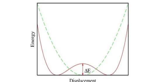
move without distorting the lattice (as show in Fig. 9 for PZT). It is a metastable structure. Appling an electric field the central atom exceeds the potential threshold and it moves to one of two octahedral spaces realizing a lower energy configuration but leading to an imbalance in the charges that is expressed in the formation of an electric dipole.
Fig. 9 One equilibrium position of energy for T>TC, green line, and two
equilibrium position of energy for T<TC, red line, in function of the
15
This behaviour can be verified below the Curie temperature (TC),
where the elementary cell is slightly distorted and tetragonal, exhibiting a non-zero dipole moment. Above TC, the elementary cell is cubic and
symmetrical, and the piezoelectric effect disappears because of the minor rigidity of the lattice due to greater atomic agitation.
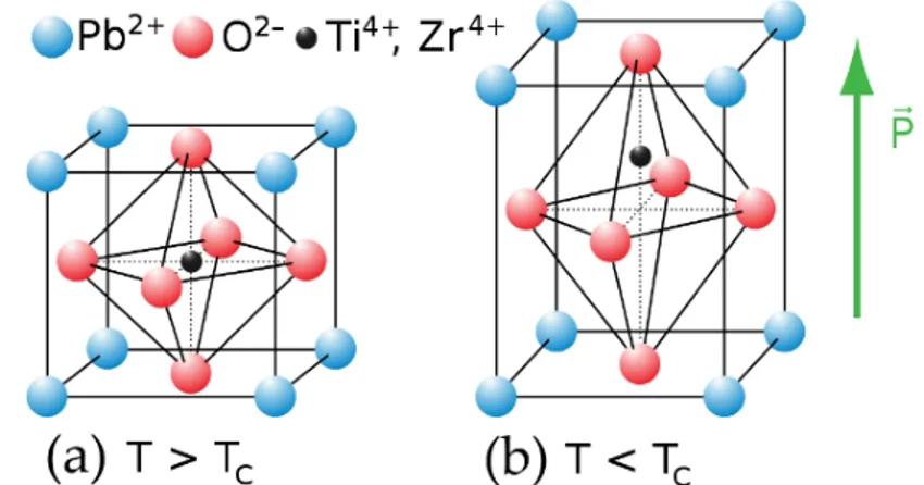
PZT is a solid solution of lead zirconate and lead titanate, often doped with other elements to obtain specific properties. PZT is produced by mixing a proportional amount of lead, zirconium, and titanium oxide powders and heating it to temperatures of 800-1000°C. During subsequent cooling phase, the cubic unit cell of the PZT becomes tetragonal. As consequence the material undergoes to a paraelectric ferroelectric phase transition. The tetragonal cell is elongated in one direction and has a permanent dipole moment oriented along its long axis (c-axis) (Fig. 10).
Fig. 10 Unit cell of perovskite crystals: paraelectric phase, T>TC (a) and
piezoelectric phase with polarization vector pointing upwards T<TC (b).
The unpoled ceramic has no net polarization because of the presence of many randomly oriented domains. Appling a high electric field (1--4 MV/cm) we can align most of the unit cells as closely parallel to the applied field as possible. This process, as said, is called “poling”. PZT exhibit typically characteristics of the piezoelectric ceramics, such us a high elastic modulus, brittleness, and low tensile strength [4].
To overcome the material’s brittleness different polymeric piezoelectric materials and nanostructured materials have been investigated. Polymers exhibit a piezoelectric effect thanks to their molecular structure and arrangement. One of the most used piezoelectric polymers is Poly(vinylidene fluoride) [PVDF; (CH2CF2)n] a
16
its chemical resistance, thermal stability, high mechanical strength, large polarization, short switching time, and peculiar electrical properties. In recent years, PVDF is widely used in organic electronics, biomedical applications, optoelectronics and energy harvesters [6–8].
In PVDF, both amorphous and crystalline phases coexist. Several crystalline phases can be identified in PVDF (α-, β-, γ-, and δ-phase). The
α-phase is non-polar and it is the most stable polymorph when PVDF is
directly cooled down from the molten state. It has, like the δ-phase, the so called TGTG’ (trans-gauche-trans-gauche) chain conformation (Fig. 11). The β-phase exhibits the strongest ferro-, piezo-, pyroelectric properties, due to its largest spontaneous polarization (7x10-30 C∙m) [9]. This phase is
generally obtained through uniaxial or biaxial stretching of melt-crystallized films [10], melt crystallization under high pressure [11], crystallization from solution under special condition [12] or through the application of high electric fields to PVDF in its α-phase [13]. Depending on the processing route, β-PVDF can be obtained in a porous or non-porous form [14]. The β-phase present the so called TTT (all trans) planar zigzag chain conformation. The γ-phase, also piezoelectric, shows the T3GT3G’ configuration (Fig. 11) [15].
Fig. 11 Schematic representation of the chain conformation for the α, β and γ phases of PVDF [15].
Among the piezoelectric nanostructured materials great interest have attracted the zinc oxide (ZnO) nanostructures, such as nanorods (NRs) and nanowalls (NWs). The ZnO nanostructures have high elasticity, hence they can be bent to a large extent. Moreover, the piezoelectric coefficient is much higher for nanostructures as compared to their bulk structure [16]. These properties make the ZnO nanostructures ideal to
17
develop a flexible nanogenerator with high performance. ZnO is an n-type semiconductor (II-VI) with a wide energy gap (3.37 eV), high exciton binding energy (60meV), high electron mobility, and unique optical, pyroelectric, and piezoelectric properties [17]. It crystallizes in three different forms: hexagonal wurtzite, cubic zincblende and the rarely observed cubic rocksalt. The hexagonal wurtzite-type structure is the most common phase of ZnO and it is showed in Fig. 12. The lattice parameters are a=0.32495 nm and c=0.52069 nm [18]. The structure is composed of several alternating planes with tetrahedrally-coordinated O2- and Zn2+ ions, stacked along the c-axis. The positively charged
Zn-(0001) polar surface and negative charged O-(0001�) polar surface are the strongest polarity surfaces. This polar surface present the piezoelectric effect: when a stress is applied, the non-central symmetric structure will lead to the separation of the central point of positive charges and that of negative charges, resulting in a net polarization [19].
Fig. 12 Hexagonal wurtzite crystal structure of ZnO.
1.3 Piezoelectric Devices
One of the most useful applications of the direct piezoelectric effect is in the field of sensors. A sensor is a device that can converts a physical quantity that is to be measured in a signal of different nature, typically electric, more easily measurable. Piezoelectric sensors are active electrical systems; it means that piezoelectric materials produce an electrical output only when there is a variation in the mechanical load (stress). For this reason, they are not able to carry out static measurements. Piezoelectric
18
sensors are used in all applications that require accurate measurement of dynamic changes of mechanical quantities such as pressure, force and acceleration. They are used in aerospace, ballistic, biomedicine, mechanical and structural engineering. The most used material to realize piezoelectric sensors is quartz (SiO2) thanks to his high resistance to the
mechanical stress, high piezoelectric thermal stability up to 500°C, high rigidity, high linearity, constant sensitivity in a wide temperature range and low conductivity. The quartz transducers are made with a layer of crystal cut along any of its axes x, y and z, depending on the specific application. Appling a force the crystal generates a charge of few pC proportional to the applied force. To pick up the electric charge, two conductive electrodes are applied to the crystal at the opposite side (Fig. 13). The piezoelectric effect is simple: when a mechanical force is applied to the crystal, the electric charges move and accumulate on the opposite faces.
Fig. 13 Piezoelctric sensor [20].
In this configuration, the piezoelectric sensor is a capacitor in which the dielectric material, in-between the metal plates, is a piezoelectric crystalline. The dielectric acts as a generator of electric charge, resulting in voltage V across the capacitor. Although charge in a crystalline dielectric is formed at the location of an acting force, metal electrodes equalize charges along the surface making the capacitor not selectively sensitive [20]. Therefore, a piezoelectric sensor is a direct converter of a
19
mechanical stress into electricity or vice versa a converter of electricity into strain.
Another important application of the piezoelectric materials is as actuator. These devices exploit the converse piezoelectric effect to convert the electrical energy in mechanical energy. For example, an electric motor is an actuator: it converts electric energy into mechanical action.
In recent years great interest was devoted to the use of piezoelectric materials to realize flexible nanogenerators. Such devices can find applications as wearable energy harvesters and sensors for smart clothing applications. Energy harvesting from ambient vibrations originating from sources such as moving parts of machines, fluid flow and even body movement, has enormous potential for small power applications, such as wireless sensors, flexible, portable, wearable electronics, and biomedical implants, to name a few. Vibrational mechanical energy is one of the most present and accessible forms of energy. Random vibrations have frequencies ranging from hundreds of Hz to kHz and the available energy density is in the range of a few hundred microwatts to milliwatt per cubic centimetre [21]. In this specific sector great interest has been attracted by piezoelectric polymers, such as PVDF ant its co-polymer such us PVDF-TrFe, semiconducting metal oxide nanomaterials such as ZnO and novel polymer-based piezoelectric composites.
1.4 Thesis Objective and Organization
Piezoelectric nanomaterials and novel polymer-based piezoelectric composites with enhanced electromechanical properties open new opportunities to the development of wearable energy harvesters and sensors for smart clothing applications.
The objectives of this thesis are:
• to develop new piezoelectric materials, suitable for the fabrication of low-cost flexible nanogenerators;
• define a characterization protocol, based on the Piezoresponse Force Microscopy (PFM), allowing quantitative evaluation of the piezoelectric response, to easily compare different materials and using simple test structures;
• demonstrate a flexible nanogenerator based on the developed piezoelectric materials.
20
Among the different emerging piezoelectric materials, we focused on two different classes of piezoelectric materials: zinc oxide nanostructures and piezoelectric polymer nanocomposites based on PVDF.
As already mentioned, Zinc oxide (ZnO) has been attracting a great deal of interest, owing to a variety of intriguing properties, along with a remarkable performance for several applications, such as piezoelectric transducers, photovoltaic devices, gas and bio-sensors, nanoscale optoelectronics and self-powered micro/nanosystems.
Poly(vinylidene fluoride) [PVDF; (CH2CF2)n] is a semi-crystalline
piezoelectric polymer. Due to its chemical resistance, thermal stability, high mechanical strength, large remnant polarization, short switching time, and unique electrical properties, PVDF has found a wide range of applications in organic electronics, biomedicine, optoelectronics and energy harvesters.
PFM technique is particularly interesting for measuring sub-picometer deformations and mapping piezoelectric domains with a lateral resolution of some nanometres. The success of this technique lies in its versatility, ease of use, non-invasiveness and the possibility of imaging the piezoelectric domains of any type of material without any particular sample preparation procedure. However, PFM does not allow to directly determine the absolute value of the piezoelectric coefficient. To this purpose, in this work, a specific protocol, based on a calibration procedure, has been proposed to provide a quantitative evaluation of the piezoelectric coefficients.
As final test vehicle a flexible piezoelectric nanogenerator has been fabricated by using as active layer the best performing piezoelectric material among those investigated. To this end, we had to also to develop advanced top electrodes, based on graphene-Au bilayers.
Moreover, various characterization techniques, such as field emission scanning electron microscopy (FE-SEM), energy dispersive X-ray analysis (EDX), X-ray diffraction (XRD), X-ray photoelectron spectroscopy (XPS), photoluminescence spectroscopy (PL) and Fourier transform infrared spectroscopy (FT-IR) have been used to probe the properties of the produced materials.
In Chapter II the principle of operation of AFM and the PFM is described. First, the two main operation modes for the AFM, contact- and tapping-mode, are discussed. Then the PFM set-up is described and it is pointed out how to perform the imaging of the piezoelectric domains. Then, a specific protocol, based on a calibration procedure, is proposed to
21
perform the quantification of the piezoelectric coefficient (d33) of the
materials studied in this thesis.
Chapter III focusses on the study of two different ZnO nanostructures namely nanorods (NRs) and nanowalls (NWs). These two nanostructured materials have been analysed in terms of morphological and chemical properties using FE-SEM, EDX and XPS. The structural analysis was assessed trough XRD and the defectivity was studied trough PL. The d33
is measured trough PFM using the calibration protocol presented in Chapter II.
In Chapter IV, in order to increase the d33 of the PVDF films, three
different nanocomposites have been studied: PVDF plus nanofillers like GNPs or ZnO-NRs; PVDF plus different HMS and PVDF plus HMS in combination with two different nanofiller either ZnO-NRs or GNPs. The morphology of the produced sample was investigated trough FE-SEM, the presence of the β-phase was assessed through FT-IR and in the sample with HMS the XRD was used to better understand the role of HMS in the formation of the β-phase. Finally, the d33 of all the produced sample was
measured.
In Chapter V the fabrication and the characterization of a flexible nanogenerator based on the best PVDF nanocomposite is presented. To guarantee high flexibility and high conductivity the top and bottom electrodes are made with a bilayer of graphene-gold (GGE). The device was successfully operating and a value of the piezoelectric coefficient of 9.00 pm/V was measured. This value was found in very good agreement with the value obtained through PFM measurements (8.88 ± 3.14) pm/V (measured without top electrode).
In Chapter VI concluding remarks on the synthesis and characterization of the different types of piezoelectric materials investigated in this thesis are reported. Future perspectives are also mentioned.
22
C
HAPTER
II
S
CANNING
P
ROBE
M
ICROSCOPY
2.1 ATOMIC FORCE MICROSCOPY2.1.1 CONTACT MODE 2.1.2 TAPPING MODE
2.2 PIEZORESPONSE FORCE MICROSCOPY (PFM) 2.2.1 HISTORY OF PFM
2.2.2 OPERATING PRINCIPLE OF PFM
2.2.3 IMAGING OF THE PIEZOELECTRIC DOMAIN
23
Chapter II
Scanning Probe Microscopy
Scanning Probe Microscopy (SPM) includes a vast range of technologies that are based on scanning a sample’s surface with a mechanical probe and it is able to give different sample's details. SPM techniques can be divided in two main categories, depending upon the feedback signal: 1) the scanning tunnelling microscopy (STM) where the current is the feedback signal and is suitable only for conducting surfaces; 2) the atomic force microscopy (AFM) where the feedback is related to the van der Waals and Pauli interactions and is suitable for all surfaces. AFM is one of the most used tools in SPM, since it allows the investigations of a wide range of surface properties on any materials, spanning from morphology to piezometric properties. In this chapter, after discussing the experimental setup and the operating principle of AFM, Piezoresponse Force Microscopy (PFM) will be explained and the experimental procedure to perform the domain imaging and the quantitative determination of the piezoelectric coefficient will be illustrated.
2.1 Atomic Force Microscopy
Atomic force Microscopy (AFM) is one of the most important SPM techniques employed to characterize a sample surface at extremely high resolution. In Fig. 14 is shows the Bruker-Veeco Dimension Icon that was used to characterize the samples.
24
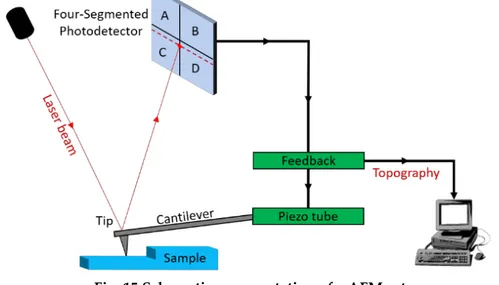
The working principle of AFM is based on the interaction between a sharp probe, a tip with a radius from 10 nm to 100 nm, placed on a cantilever, that is lead into proximity with the sample to be analysed. The interaction between tip and sample leads to a deformation of the cantilever. During the interaction between tip and sample two kinds of atomic forces are involved: at large distance the van der Waals force is the dominant one; at short distance the repulsive Pauli force is the dominant one. Probe and sample are moved relative to each other in a raster pattern, each line of the selected area is scanned forth (trace) and back (retrace), then the cantilever following the topography of the sample give back the morphology of the sample itself. A feedback loop controls the cantilever’s deformation, controlling a piezoelectric actuator (Z scanner), which keeps either the tip at a constant distance from the surface or tip contact force constant (depending on the used scanning mode). The cantilever deformation is detected trough a laser beam, focused onto the backside of the probe, then reflected and collected through a photodetector, consisting of four different photodiodes. This setup is called beam deflection method, which measure the displacement with respect to the equilibrium beam position. In Fig. 15 a schematic representation of the AFM setup is reported.
Fig. 15 Schematic representation of e AFM setup.
The angular displacement of the cantilever results in a variation of the laser spot position on the photodetector, corresponding in one
25
photodiode which collect more light then the other, generating an output signal. The deformation can be due to a vertical or lateral force (Fv and
Fl). The photodiode, measuring the intensity A, B, C and D of the reflected
laser beam, can distinguish the signals of vertical and lateral forces as follows:
Vertical Signal: 𝑆𝑆v= (𝐴𝐴+𝐷𝐷)−(𝐵𝐵+𝐶𝐶)(𝐴𝐴+𝐵𝐵+𝐶𝐶+𝐷𝐷) (2.1)
Lateral Signal: 𝑆𝑆𝑙𝑙 = (𝐴𝐴+𝐵𝐵)−(𝐶𝐶+𝐷𝐷)(𝐴𝐴+𝐵𝐵+𝐶𝐶+𝐷𝐷) (2.2)
The difference between the sum of the signal of the top two elements and the two bottom elements provides the measure of the vertical deflection Sv of the cantilever while the difference between the sum of the
two left elements and the sum of the two right elements provides the measure of the torsion of the cantilever SL. In Fig. 16 is sketched the
cantilever deformation that correspond to the vertical and lateral deflection.
Fig. 16 Vertical and lateral forces (Fv and Fl) acting on the tip (a);
deformation of the cantilever and corresponding deviation of the laser spot (b) [22].
The two principal operating modes for the AFM are: contact mode and tapping mode.
2.1.1 Contact Mode
Contact mode is the basic and fundamental AFM mode and it is used to measure a series of surface properties, including conductive AFM and PFM. Extending the Z scanner, the probe approaches the surface of the sample. Once the tip is in contact with the sample the cantilever starts to
26
bend. When the cantilever deflection reaches the defined setpoint, that corresponds to a predetermin contact force, the extinction of the Z scanner stops. The scanning over the sample’s surface causes the cantilever deflection to change. In this case the feedback element controls the Z scanner in a way that the force between sample and tip is kept constant to a chosen setpoint. This procedure provides the topography information which is visualized by a computer [22].
The interaction between tip and surface can be expressed by the Lennard-Jones potential that, as well known, is the result from the combination of the terms: an attractive interaction Van-der-Walls force and a repulsion interaction Pauli force (see Fig. 15). During the probe approach, the attractive Van-der-Waals interaction is dominant. At short distance the Pauli repulsion overcomes the attraction. In the contact mode the distance is z ≪ 1 nm where the repulsive forces control the cantilever deformation. The steep trend of the potential guarantees a high vertical resolution [22].
Fig. 17 Lennard-Jones potential U(z) for two atoms with distance z [22].
The contact force can be estimated performing the so-called force plot procedure. In order to perform this measurement, the Z scanner has to make, without any feedback, two different movements: first the probe approaches the surface and then retracts from it. In Fig. 18 a typical force curve is reported: the deflection of the cantilever is plotted as a function
27
of the of the position of the Z scanner. From the non-contact position, the probe goes down until it touches the surface. The cantilever is not bent, and there is no tip-sample contact and the beam is in its equilibrium position (blue line, segment 1), until the attractive forces, in proximity of the surface, pull down the tip. The tip starts to be in contact with the sample and the cantilever bends downwards, with a decrease in deflection (segment 2). Once in contact, the probe descends further producing an increasing of the contact force, and the cantilever bends upward resulting in an increase of the deflection (segment 3). When the Z scanner is moving in the reverse direction, the probe starts ascending, the force decreases, and the cantilever relaxes (red line, segment 4). Attractive capillary forces between tip and surface make the tip to hold on it, causing the cantilever to bend downward (segment 5). The deflection decreases further until the spring force of the cantilever overcomes the attractive forces (segment 6) at the pull-up point. The cantilever comes back to the non-contact position (segment 7).
Fig. 18 Typical force curve. The red line represents the response during the tip approaching while the blue line is the response during the retracting.
The deflection setpoint determines the contact force. From the force curve it is possible to calculate the contact force maintained by the feedback loop during the measurement. The vertical deflection of the cantilever coincides to the Z scanner movement. If the cantilever spring constantan k is known, using the Hooke’s law it is possible to calculate the contact force:
28
where Δz is the distance covered by the Z scanner to bring the cantilever deflection from the setpoint to the pull-up point. Typical contact forces are in the range of 10-9 N.
In contact mode AFM there are high lateral forces between the tip and the surface that can damage the tip or the sample surface. To overcome this problem the tip can touch the sample's surface only for a short time using a so-called tapping mode AFM.
2.1.2 Tapping Mode
Tapping mode AFM operates by scanning a tip attached to the end of an oscillating cantilever across the sample surface. The cantilever is oscillated at or slightly below its resonance frequency with an amplitude ranging typically from 20 nm to 100 nm. A typical response curve of a cantilever is shown in Fig. 19. When the tip is close to the surface, because of their interaction, the resonance shifts to lower frequencies and exhibits a drop-in amplitude. The tip lightly “taps” on the sample surface during scanning, contacting the surface at the bottom of its swing. The feedback loop maintains a constant oscillation amplitude by maintaining a constant RMS of the oscillation signal acquired by the split photodiode detector. The photodetector sends the signal to an internal lock-in amplifier (LIA), which yields a DC signal proportional to the amplitude of the cantilever
Fig. 19 Resonance curve of a tapping mode cantilever above (a) and close to the surface (b) [23].
29
oscillation. To maintain constant the amplitude oscillation the feedback control drives a piezo-tube to adjust the vertical position of the cantilever. The vertical position of the scanner at each (x,y) data point is stored by the computer to form the topographic image of the sample surface. By maintaining a constant oscillation amplitude, a constant tip-sample interaction is maintained during imaging. A schematic representation of the tip oscillation, without feedback loop (a) and with feedback loop (b), for two different average tip-sample distance is reported in Fig. 20.
Fig. 20 Tip oscillation without feedback loop (a) and with feedback loop (b) for two different average tip-sample distances dA and dB. The oscillation
remains sinusoidal also at reduced distances d [24].
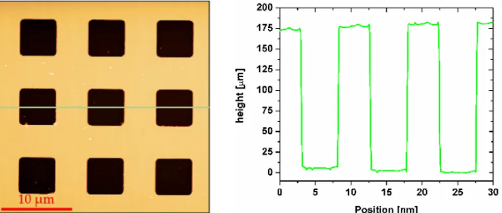
Fig. 21 shows the topography of a calibration grating with 10 µm pitch and 180 nm step height.
Fig. 21 Topography of a calibration grating with 10 µm pitch and 180 nm step height(a) and heigt profile along the green line (b).
It should be pointed out that, thanks to the LIA technique, the tapping mode guarantees a higher lateral resolution respect to the contact mode.
30
2.2 Piezoresponse Force Microscopy (PFM)
Piezoresponse Force Microscopy (PFM) is an AFM technique able to record the piezoelectric response of a sample. The technique allows to detect the piezoelectric amplitude and phase imaging with high resolution, down to 0.1 nm. The mechanisms contribution to the contrast in PFM imaging are still under debate in literature and can hardly be used for quantitative measurements. In this thesis PFM has been applied to quantitatively evaluate the piezoelectric coefficient of the different investigated materials.
2.2.1 History of PFM
PFM was introduced to measure the local piezoelectric coefficient at the nanoscale as a non-destructive method. In the ideal case, the electromechanical response can be linked to the local piezoelectric response.
At the beginning of the 90s some research groups started to modify the AFM setup. To detect the polarization in ferroelectric samples they used a tip as movable electrode. In 1991 the Dransfeld’s group [25] using a scanning tunnelling microscope (STM) measured the piezoelectric coefficient of a vinylidene fluoridetrifluoroethilene (VDF-TrFE) sample provided with a top gold electrode. One year later [26] they developed an AFM using the tip as top electrode for both polarizing and detecting polarization in VDF-TrFE.
Since then a great attention was focused on ferroelectric materials in view of data storage applications. PFM evolved with the combination of vertical and lateral PFM, and the area of research expanded over PZT thin films and different materials [27]. In order to have a proper interpretation of the PFM data a lot of groups started to study the process underlying PFM measurements. Among those, in 2006, Jungk et al. [28] developed a vectorial analysis of the PFM mechanism to detect the piezoresponse signal. In particular they pointed out how the presence of a background noise, coming from the experimental setup, is responsible of many irregularities in PFM measurements.
31
2.2.2 Operating Principle of PFM
PFM is based on the standard contact mode AFM setup, schematically sketched in Fig. 22. The imaging contrast for domains is based on the converse piezoelectric effect.
Fig. 22 Schematic representation of the piezoresponse force microscopy (PFM).
In addition to the standard AFM setup, an alternating voltage is applied between the mandatorily conductive tip and a back electrode behind the sample. The alternating voltage can also be applied to the back-electrode (BE) while grounding the tip. Such an interchange results only in a phase shift of π of the lock-in output signal.
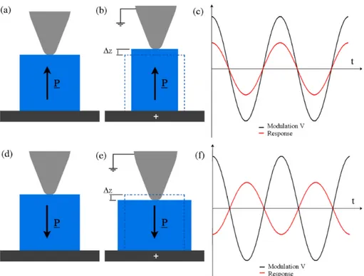
The modulation voltage generates an alternating field across the sample, which makes it to vibrate. The phase Θ of such a vibration depends on the polarization direction inside the sample. If the latter is in phase with the applied field, the vibration of the sample is in phase with respect to the modulation voltage (Θ = 0). Conversely, for opposite mode it is out of phase (Θ = π, see Fig. 23).
The BE, that is grounded, guarantees a well defined electric field distribution and thereby reproducible conditions for PFM imaging. The piezoelectric samples respond to the alternating electric field with a periodic deformation. Consequently, according to the piezoelectric
32
Fig. 23 Phase shift in piezoresponse: for a upward polarization (a), the volume expand for an upward field (b) and the vibration is in phase with the
excitation voltage (c). For a downward polarization domain (d), the volume contracts for upward field (e) and the vibration is out of phase with the
modulation voltage (f) [27].
coefficients the sample will be deformed and this deformation will be followed by the tip. The probe displacement, due to the deformation, is recorded via the photodiode. In order to separate the topography and piezoresponse signal, a lock-in amplifier (LIA), which also acts as a sharp band pass filter, is required. The LIA compares the response signal with the reference signal and amplifies only the frequency component that is equal to the reference signal. Since the reference signal and the voltage applied to the tip have the same frequencies, the expected piezoresponse is also at the same frequency. This allows measurements with a high signal-to-noise ratio even for small signals, like average displacements of just a few picometers (pm). Generally, the amplitude is set to values up to 10 V and the frequency from 10 kHz to 100 kHz. PFM can measure both out-of-plane and in-plane components of the piezoresponse [29], performing complementary measurements called vertical PFM (VPFM)
33
Fig. 24 Possible movements of the cantilever due to forces acting on the tip. Flexural deflection (left), detected in VPFM, originates from an out-of-plane
piezoresponse. Flexural buckling (centre), detected in VPFM, and lateral twisting (right), detected in LPFM, both originate from an in-plane piezoresponse. The double arrows in the upper part of the figure represent
changes in the laser spot position on the photodiode. The solid double arrows in the lower part represent the cantilever motion, while the dashed
double arrows represent the motion of the sample surface acting of the cantilever [29].
and lateral PFM (LPFM). As showed in Fig. 24, VPFM detects vertical movements of the laser position on the photodiode, associated with the flexural deflection or buckling of the cantilever, while LPFM detects the lateral movements of the laser position, associated with the lateral twisting of the cantilever.
Flexural deflection is caused by an out-of-plane piezoresponse (deformations in the z direction), but flexural buckling is caused by an in-plane piezoresponse parallel to the cantilever axis (deformations in the y direction). Lateral twisting is caused by an in-planepiezoresponse perpendicular to the cantilever axis (deformations in the x direction).
2.2.3 Imaging of the Piezoelectric Domains
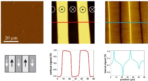
Periodically poled lithium niobite (PPLN) is a very useful sample to demonstrate the relationship between polarization orientation and
34
piezoresponse, since it exhibits a simple 180° domain structure, as sketched in Fig. 25. Furthermore, in Fig. 25 are reported the corresponding vertical and lateral PFM signals.
Fig. 25 Morphology and domain structure of PPLN (a), vertical (b) and lateral (c) PFM signal domain image and the relative profile, respectively along the
red and the blue line.
The two 180° domains cause a 180° phase shift in the respective vertical piezoresponse. This results in a positive and negative DC signal from the LIA, respectively, that is visible as a contrast in the vertical PFM image (Fig. 25 (b)). Since for z-cut PPLN the polarization is always perpendicular to the sample surface, there is a lateral signal that which produces a peak-like structure at the domain boundaries, as can be seen in Fig. 25 (c) [30].
2.2.4 Quantification of the Piezoelectric Coefficient
PFM is well used to detect the ferroelectric domain patterns with a high lateral resolution of about 10 nm and has also proven to be extremely sensitive as it allows measurement of local surface displacements in the sub-pm regime [31]. Nevertheless, there is still lack of an opportune procedure to determine the absolute values of the piezoelectric coefficient with high precision. In this thesis a procedure to quantitative evaluate the piezoelectric coefficient (d33) is proposed and applied to a variety of
samples. In the PFM measurements, thanks to the LIA, a periodic signal from a noisy environment can be extracted and rectified and comparing it with an external reference frequency a phase Θ can be attributed to the
35
signal. The LIA measurement can be presented either as two amplitudes (X, Y) or as magnitude and phase (R, Θ). These two representation are connected by X = R sin Θ and Y = R cos Θ [31]. It has to be pointed out that the LIA determines (X, Y) electronically and calculate (R, Θ) in a successive step. A useful way to understand the evaluation of the background is to use a x–y-representation on an oscilloscope of the X- and
Y -output LIA signals (see Fig. 26).
Fig. 26 x/y-representation of the PFM signal obtained on a PPLN sample with piezoresponse d in the case of no background (a) and with background (b)
[31].
A PPLN sample, that is characterized by two-domain (↑↓) (see Fig. 25) with a piezoresponse +d and -d, is used as test sample. The alternating voltage V𝑎𝑎𝑐𝑐, applied to the tip, fixed the external reference frequency.
When the output LIA signal is background free the magnitudes R on both domains are the same and their relative phase difference is ∆𝛩𝛩 = 180°, as sketched in Fig. 26 (a). When a background 𝐵𝐵�⃗ is present the origin of the Cartesian coordinate system is shifted to a new position by the vector 𝐵𝐵�⃗. The consequence is that the magnitude R of the PFM signals on the two domains are no longer equal, and their phase difference ∆𝛩𝛩 ≠ 180° [31]. A simple way to overcome the background problem consists in recording the X-output signal of the LIA for PFM imaging. Since any contribution to the PFM signal caused by the piezoresponse from the PPLN must be either in phase or 180° out of phase with respect to the V𝑎𝑎𝑐𝑐, any
information in the Y-output must be either due to the background or to an electronic delay in the electronics of the system. The X-output signal of the LIA therefore contains the complete information of a PFM measurement.
36
The PFM technique gives us both the phase Θ and the magnitude R of the LIA output channels. The Θ output of the LIA, as said before, gives us only two values: 0° and 180°, even if the polarization vector is not oriented normal to the sample surface but at a certain angle φ (see Fig. 27 (a)), the Θ output of the LIA yields only these two values. The magnitude of the output R presents the displacement at the sample surface. The amplitude output X contains both the phase and the magnitude information. In the case of a background the Θ output can exhibit values different from 0° and 180°. In this case we need to estimate the background and subtract it from the PFM measurements [28]. Briefly, the procedure is based on the evaluation of the vertical PFM signal of the PPLN. If the VPFM signal of PPLN is symmetric respect to the vertical signal axis (see Fig. 25), the background is nought. Otherwise, the background signal is the mean value between the highest and the lowest value of the VPFM, for each applied voltage value.
In Fig. 27 the LIA output signals Θ, R and X are shown for a sample exhibiting seven domains with the polarization pointing into different directions. It can be seen that the combination of the Θ and R output signals yields the same information as the X output signal on its own.
Fig. 27 Sample with polarization vector oriented at the angle ϕ with respsct to the surface sample (a). Phase Θ, magnitude R and amplitude X of a sample
37
The deformation at the surface of the sample, Δz, due to the converse piezoelectric effect, is a linear function of the amplitude of the applied a.c. voltage V𝑎𝑎𝑐𝑐:
𝛥𝛥𝑧𝑧 = 𝑑𝑑𝑖𝑖𝑖𝑖 𝑉𝑉ac (2.4)
in which 𝑑𝑑𝑖𝑖𝑖𝑖 is the local relevant element of the third-rank piezoelectric
tensor of the material [32]. The raw amplitude signal, measured using the segmented photodiode and LIA, is converted to a displacement amplitude by applying a calibration factor, which is obtained through the measurement of a calibration piezoelectric material. To this purpose a Bruker reference sample, consisting of a periodically poled lithium niobate (PPLN) specimen, with an effective piezoelectric coefficient 𝑑𝑑33_PPLN= 7.5 pm/V, is employed. In the ideal case the amplitude of the
measured piezoresponse X depends linearly from Vac:
𝑋𝑋 = 𝜉𝜉 𝑑𝑑33 𝑉𝑉ac (2.5)
in which 𝜉𝜉 is a calibration parameter, 𝑑𝑑33 is the effective piezoelectric
coefficient measured via PFM and 𝑉𝑉𝑎𝑎𝑐𝑐 is the amplitude alternating
voltage. In order to estimate 𝜉𝜉 the background correction technique, briefly outlined above and discussed in in more detailed in [31], is applied. At first, six areas at the same point of the specimen were scanned, with a scan area (60×7.5) µm2 in size with (256×32) measured points with
an applied alternating voltage at a fixed frequency (10 kHz ≤ 𝑓𝑓 ≤ 100 kHz, typically 15 kHz) and increasing amplitude from 0 V to 10V with a step of 2V. The amplitude of the PFM signal (X) resulting from the average of the (256×32) measurement points over the scanning area is plotted as a function of 𝑉𝑉𝑎𝑎𝑐𝑐 (see Fig. 28). Then, through a linear fitting of
the straight line the slope of the calibration sample (𝑚𝑚PPLN) is evaluated
and the calibration factor is estimated:
𝜉𝜉 = 𝑚𝑚PPLN⁄𝑑𝑑33_PPLN (2.6)
where 𝑑𝑑33_PPLN is the known piezoelectric coefficient of the PPLN.
Finally, the response of the sample under test is measured and using 𝜉𝜉 we convert the X signal (expressed in V) into the vertical displacement (Apiezo):
38
.Fig. 28 Measured amplitude of the piezoresponse of PPLN with respect to the applied voltage Vac.
Using the well-known equation of the converse piezoelectric effect (𝐴𝐴𝑝𝑝𝑖𝑖𝑖𝑖𝑖𝑖𝑐𝑐= 𝑑𝑑33∙ 𝑉𝑉𝑎𝑎𝑐𝑐) evaluating the slope (m) of the Apiezo in function of the
Vac, through a linear fitting, we estimated the 𝑑𝑑33:
𝑑𝑑33 = 𝑚𝑚 =𝐴𝐴𝑝𝑝𝑝𝑝𝑝𝑝𝑝𝑝𝑝𝑝𝑉𝑉𝑎𝑎𝑎𝑎 (2.8)
After completing the PFM characterization of the desired sample, the reference PPLN was tested again in order to verify that the system was still calibrated. For this purpose, we repeated the measurement of the piezoelectric signal (𝑋𝑋) of the reference PPLN sample and we compared the new value with the corresponding value previously measured (before the characterization of the desired sample). If the difference between the two calibration piezoelectric signals for each value of the applied voltage 𝑉𝑉𝑎𝑎𝑐𝑐is less than 20%, the measurement of the sample under test is
considered reliable. Differences larger than 20% may occur due to several instabilities, including tip degradation, drift of the electronic apparatus or of the thermal and noise conditions.
The proposed protocol can be then schematically summarized as follows:
• First a calibration measurement of the PPLN sample, with known
d33, is conducted in the amplitude voltage range at which the sample
39
• Then the sample under test is measured in the selected amplitude voltage range;
• The PPLN is measured again and the new VPFM signals, for each value of the applied voltage 𝑉𝑉𝑎𝑎𝑐𝑐, are compared with the
corresponding values measured during the first calibration cycle; • If the difference between the two piezoelectric calibration signals is
less than 20%, the measurement of the sample under test is considered reliable;
• Then the calibration factor 𝜉𝜉 is evaluated, averaging over the two calibration measurements, and the d33 value of the sample under test
40
C
HAPTER
III
Z
INC
O
XIDE
N
ANOSTRUCTURES
3.1 INTRODUCTION3.2 PRODUCTION OF ZNO NANORODS
3.3 CHARACTERIZATION OF ZNO NANORODS
3.3.1 MORPHOLOGICAL AND CHEMICAL CHARACTERIZATION 3.3.2 STRUCTURAL ANALYSIS
3.3.3 CHEMICAL COMPOSITION
3.3.4 PHOTOLUMINESCENCE PROPERTIES 3.3.5 PIEZOELECTRIC PROPERTIES
3.4 PRODUCTION OF ZNO NANOWALLS
3.5 CHARACTERIZATION OF ZNO NANOWALLS
3.5.1 MORPHOLOGICAL AND CHEMICAL CHARACTERIZATION 3.5.2 STRUCTURAL ANALYSIS
3.5.3 CHEMICAL COMPOSITION
3.5.4 PHOTOLUMINESCENCE PROPERTIES 3.5.5 PIEZOELECTRIC PROPERTIES
41
Chapter III
Zinc Oxide Nanostructures
Zinc oxide (ZnO) nanostructures, such as ZnO nanorods (NRs) and nanowalls (NWs), have attracted a great interest to fabricate devices for energy harvesting, thanks to their capability to convert the ambient vibrational energy into electrical energy. In this chapter, after a brief description of the synthesis method of ZnO NRs and NWs, structural, crystalline, chemical electronic and piezoelectric properties of the materials are analysed.
3.1 Introduction
Several methods have been developed to grow ZnO nanostructures [33–38]. Among them chemical bath deposition (CBD) [35–37] has received much attention, as it ensures a high deposition rate on a wide variety of substrates; moreover, it is facile, cost-effective and easy to scale-up. The properties of ZnO nanostructures are strongly depending on their size, shape, and morphology [36,39–41]. In particular, the characterization of the piezoelectric properties of ZnO nanostructures having different morphology is a fundamental step towards the production and performance optimization of nano-generators and nano-actuators.
3.2 Growth of ZnO Nanorods
In this thesis the ZnO NRs are grown using a facile CBD, developed by Chandraiaghari during his PhD thesis [19,42]. All chemicals are of reagent grade and used as obtained from the manufacturer: zinc acetate dihydrate (Zn(CH3COO)2⋅2H2O, Sigma-Aldrich, ≥ 98%), zinc nitrate hexahydrate
(Zn(NO3)2⋅6H2O, Acros Organics, 98%), hexamethylenetetramine
(HMTA, C6H12N4, Fisher Scientific, ≥99%), isopropanol ((CH3)2CHOH,
Sigma-Aldrich, ACS reagent, ≥ 99%), acetone (CH3COCH3, Acros
Organics, ≥ 99%) and deionized water (DI) with a resistivity of 18 MΩ⋅cm. The substrates, generally glass or polyethylene terephthalate (PET) covered with a thin film of indium tin oxide (ITO), are first cleaned in acetone and then in isopropanol. Subsequently they are dried in an oven at 70 °C for 10 min. Prior to growth, a seed layer is deposited onto the
42
cleaned substrates by the dip-coating method. A seed solution is prepared by dissolving 5 mM of zinc acetate dehydrate in to 40 ml of isopropanol using magnetic stirring at room temperature. The substrates were then dip-coated in the seed solution and underwent thermal annealing inside a muffle furnace at 300 °C for 30 min, in the case of a PET/ITO as a substrate the thermal annealing is inside a furnace at 150 °C for 30 min. This process resulted in substrates coated uniformly with ZnO seed particles having an average diameter of 20 nm (see Fig. 29) [42].
Fig. 29 FE-SEM micrograph of the ZnO seed particles.
ZnO nanostructures are grown on the seeded substrates using CBD [32]. Briefly, an aqueous growth solution is prepared by dissolving 20 mM equimolar ratios of zinc nitrate hexahydrate and hexamine together in 100 ml of DI water. The seeded substrate was then vertically immersed into the growth solution. The suspension was placed on a hot plate (Heidolph MR-Hei Standard) under static conditions for 4.5 h. During the reaction, the beaker was sealed with an Al foil and the solution temperature was fixed at 60 °C using an automatic electronic temperature controller (EKT Hei-Con). After Zn nitrate dissociation, Zn2+ ion forms a complex with six
water molecules [Zn(H2O)6]2+. The essential equations for the description
of ZnO-NRs growth is the following [37]:
[Zn(H2O)]2++ H2O ↔ [Zn(H2O)5OH]++ H3O+ (3.1)
[Zn(H2O)5OH]++ H2O ↔ Zn(OH)2(s)+ H3O++ 4H2O (3.2)
![Fig. 11 Schematic representation of the chain conformation for the α, β and γ phases of PVDF [15].](https://thumb-eu.123doks.com/thumbv2/123dokorg/2894563.11498/24.744.115.638.500.718/fig-schematic-representation-chain-conformation-a-phases-pvdf.webp)