UNIVERSITY OF CALABRIA
Department of Engineering for the Environment and the Territory and Chemical Engineering
Ph.D. Course
Science and Engineering of the Environment, the Structures and the Energy
CYCLE XXXI
Random Telegraph Signal in CMOS Single Photon Avalanche
Diodes
SSD ING-INF/01 ING-IND/20
Coordinator: Prof. Salvatore Critelli
Supervisore/Tutor: Prof. Calogero Pace Prof. Felice Crupi
Dott. Francesco Di Capua
Prof. Elio Angelo Tomarchio
Ph.D. Candidate: Dott./ssa Daniela Fiore
i
Contents
Abstract……… 1
1. Photon Detectors in CMOS Technology………. 3
1.1 Photosensor properties……….. 4
1.2 Avalanche photodiodes……….. 6
1.3 Single Photon Avalanche Diodes……….. 8
1.3.1 SPAD performance parameters………...……….. 9
1.3.2 Quenching circuit………...11
1.4 SPAD architectures ... 13
1.5 CMOS SPAD technology ... 16
1.6 Silicon Photomultipliers ... 18
1.7 SPAD Noise Performance ... 20
1.7.1. Afterpulsing events………20
1.7.2. Crosstalk………. ... 23
2 Noise Sources ... 25
2.1 Shockley-Read-Hall thermal processes ... 28
2.2 Tunneling process ... 31
ii
2.4 Diffusion from neutral region ... 36
2.5 Radiation effects ... 37
2.5.1. Total Ionizing effect………. 37
Displacement Damage effect………. ... 40
Niel Scaling……….. 43
2.6 Random Telegraph Signal ... 45
Probability distribution of RTS ……… 46
1/𝑓 noise ……… 49
Time Lag Plot ……… ... 52
Surface and bulk damage in semiconductor ….………..……..53
Hypotheses for RTS origin ………57
Annealing process ……….65
3 SPADs characterization ... 67
3.1 SPAD device under test ... 67
3.1.1 SPAD depletion region………. ... 73
3.2 Experimental setup ... 75
3.3 Dark Count Rate Measurements ... 76
3.4 Activation energy... 80
4 Random Telegraph Signal Investigation ... 86
4.1 Proton irradiation test ... 87
iii
4.3 RTS in time and frequency domain………..…. ... 92
4.4 RTS measurements ... 102 4.5 RTS amplitudes ... 104 4.6 RTS Time Constants ... 108 4.7 Annealing ... 110 4.7.1 DCR and RTS annealing………...111 Conclusion ... 117 Bibliography ... 120
iv
List of Figures
Figure 1-1. Absorption coefficient as a function of incident light wavelength for semiconductor material………...6
Figure 1-2. a) Current-voltage characteristic; b) Description of working processes in SPAD………. 8 Figure 1-3. Schematic representation of SPAD with equivalent circuit… ... 11 Figure 1-4. Basic circuit of SPAD with passivea) and activeb) quenching circuit...13 Figure 1-5. Structure of Reach-Trough SPAD……. ... 14 Figure 1-6. Structure of planar SPAD… ... 15 Figure 1-7. a) N+ layer between n substrate and p surface, b) low doped p guard ring enclosing the junction, c) low-doped n region between p area, d) structure with STI guard ring…… ... 17 Figure 1-8. Scintillation light detector systems based on the analog (a) and digital (b) silicon photomultiplier.. ... 19 Figure 1-9. Mechanism of trapping and delayed realising of a free carrier by an impurity in the depletion region (afterpulsing event) ... 21 Figure 1-10. Afterpulsing events introducing a short a) or long b) dead time after first carriers avalanche ... 22 Figure 1-11. Optical Crosstalk between neighbouring pixels……… ... 23 Figure 1-12. Direct a) and reflected b) optical path at bottom of substrate ... 24 Figure 2-1. Source of noise in SPADs: a) thermal generation, b) trap-assisted thermal generation, c) band-to-band tunneling, d) trap-assisted tunneling, e) direct thermal generation and diffusion ... 26
v
Figure 2-2. Processes involved in the Shockley Read Hall model: a) electron capture, b) electron emission, c) hole capture, d) hole emission ... 29 Figure 2-3. Tunneling probability variation in a) small electric field and b) large electric field ... 33 Figure 2-4. Schematic representation of Poole-Frenkel effect ... 34 Figure 2-5. Basic radiation-induced processes at Si-SiO2 ... 38
Figure 2-6. Point defect damage in silicon with vacancy and interstitial atoms .. 41 Figure 2-7. NIEL as a function of energy for electrons, pions, neutrons and protons ... 44 Figure 2-8. RTS behaviour with parameters: 𝝉𝒖𝒑,𝝉𝒅𝒐𝒘𝒏,𝑨𝑹𝑻𝑺 ... 47
Figure 2-9. a) RTS noise power spectral density (Lorentzian shape) and b) corresponding current fluctuactions ... 50 Figure 2-10. The summation of RTS noise results in a 1/f noise spectrum in the frequency domain ... 52 Figure 2-11. Schematic explanation of Time Lag Plot ... 53 Figure 2-12. Energy versus defect configuration for a defect with two stable states A and B. In one charged state (thick line) state A has the lower energy. In the other (thin line), B is the more stable ... 58 Figure 2-13. The silicon lattice containing the E-center defect ... 60 Figure 2-14. Schematic representation of intercenter transfer mechanism with diagram of SRH generation ... 63 Figure 2-15. Structures of trapped vacancies and their electrical level positions .. ... 64 Figure 2-16. Intercenter transfer mechanism in case of two adjacent divacancies. Each energy level in the bandgap corresponds to the energy levels in Fig. 2.15 .. ... 64
vi
Figure 2-17. Vacancy and vacancy-defect pair annealing stages... 66
Figure 3-1. Layout of PN layout (P+/Nwell junction) ... 68
Figure 3-2. Layout of PWNISO1 layout (Pwell/Niso junction)... 69
Figure 3-3.Layout of PWNISO2 layout (Pwell/Niso junction) ... 69
Figure 3-4. Array block with 8 linear arrays ... 70
Figure 3-5. Square SPADs matrix with cut corners ... 70
Figure 3-6. a) Cross section of PN layout; b) Cross section of PWNISO layout ... 71
Figure 3-7. Schematic SPAD front-end circuit ... 73
Figure 3-8. Cross section and simplified doping profile of PN (a) and PWNISO (b) layout ... 73
Figure 3-9. Simulated electric field in PN (left) and PWNISO (right) layout ... 75
Figure 3-10. Schematic diagram of experimental setup ... 76
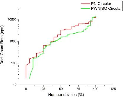
Figure 3-11. Dark Count Rate in circular PN and PWNISO layout ... 77
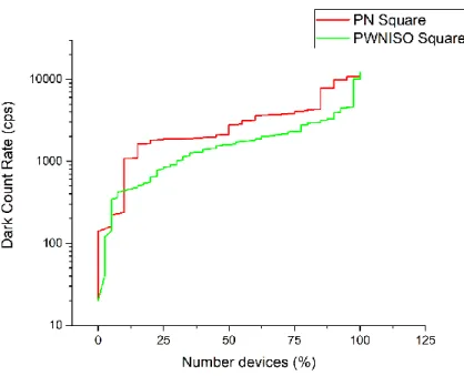
Figure 3-12. Dark Count Rate in square PN and PWNISO layout ... 78
Figure 3-13. DCR vs. time behaviour of four pixels before irradiation ... 79
Figure 3-14. Dark Count Rate as a function of temperature in PN and PWNISO layout... 79
Figure 3-15. Dark Count Rate as a function of Bias Voltage at different temperatures in PN (a) and PWNISO (b) layout ... 80
Figure 3-16. Breakdown voltage as a function of temperature for PN (a) and PWNISO (b) layout ... 81
Figure 3-17. Dark Count Rate as a function of overvoltage at different temperatures in PN (a) and PWNISO (b) layout ... 81
vii
Figure 3-19. Arrhenius plot of PWNISO SPAD at Vov=3V ... 83
Figure 3-20. Activation energy as a function of Dark Count Rate at 20°C for different PN and PWNISO pixels ... 85
Figure 4-1. Proton irradiation test at Tandem accelerator: experimental setup with the boarding test (a) and the beam stopper and ionization chamber on the beam line (b) ... 88
Figure 4-2. Ionization chamber output current vs. beam current ... 89
Figure 4-3. GAFchromics film EBT3 impressed by proton beam ... 89
Figure 4-4. Dose profile of irradiated GAF EBT3 ... 90
Figure 4-5. Proton irradiation test at Cyclotron accelerator ... 91
Figure 4-6. Mean DCR as a function of Displacement Damage Dose on several proton irradiated chips ... 93
Figure 4-7. DCR cumulative distribution for 25 SPADs with 10 μm active region at Vov = 3.4 V ... 93
Figure 4-8. Power Spectral Density of RTS pixel with 1/f (green) and 1/f2 slope (red) ... 94
Figure 4-9. Bi-level RTS (left) and multi-level RTS behaviour (right) ... 95
Figure 4-10. Dark Count Rate as a function of time in RTS pixel ... 96
Figure 4-11. Time up and time down distribution of bi-level RTS pixel ... 96
Figure 4-12. Variation of time constants and amplitude by changing the temperature ... 98
Figure 4-13. Bi-levels RTS Gaussian curve ... 98
Figure 4-14. TLP of bi-level RTS in Fig. 4.10 ... 100
viii
Figure 4-16. a) Bi-levels RTS and b) corresponding TLP ... 101 Figure 4-17. a) Bi-levels in bi-levels RTS and b) corresponding TLP ... 102 Figure 4-18. Dark Count Rate histogram for all pixel population (red) and for RTS pixel (blue) ... 104 Figure 4-19. Dark Count Rate vs. OverVoltage in PN and PWNISO pixel in High (a) and Low (b) RTS level ... 105 Figure 4-20. RTS behaviour at different SPAD reverse bias with 0.2 V increasing step ... 106 Figure 4-21. RTS amplitude as a function of temperature for PN and PWNISO pixel ... 107 Figure 4-22. Time constant in the high level 𝝉𝒖𝒑 (a) and in the low level 𝝉𝒅𝒐𝒘𝒏 (b) as a function of temperature in PN and in PWNISO layout ... 109 Figure 4-23. Evolution of DCR annealing at different temperatures for PN and PWNISO layout ... 112 Figure 4-24. Evolution of RTS pixels annealing at different temperatures for PN and PWNISO layout ... 112 Figure 4-25. Distribution of RTS PWNISO pixels at different annealing temperatures ... 113 Figure 4-26. Evolution of a bi-level (a) and multilevel RTS during annealing. No RTS behaviour occurs at 𝟏𝟓𝟎 °𝑪 ... 115 Figure 4-27. Evolution of a bi-level RTS during annealing. RTS behaviour persists at 𝟐𝟓𝟎 °𝑪 ... 116
ix
List of Tables
Table 2-1. Some defect reactions in silicon. The i subscript stands for interstitials,
s for substitutional, I for Si interstitials, V for vacancy, C for carbon, O for oxygen
and P for phosphorus ... 59
Table 2-2. Energy levels in eV of some defect states. The subscript c stands for conduction and v for valence ... 60
Table 3-1. Geometrical features of SPADs ... 71
Table 3-2. Geometrical features of SPADs array ... 72
Table 3-3. Geometrical features of SPADs matrix ... 72
Table 3-4. Average Dark Count Rate in circular and square layout ... 77
Table 3-5. Activation energy values for PN and PWNISO layout at positive and negative temperatures ... 82
Table 4-1. Chip 5 proton irradiation runs... 90
Table 4-2. Total Ionizing Dose (TID) and Displacement Damage Dose (DDD) for analysed pixels ... 92
Table 4-3. Classification of RTS pixels and of the number of RTS levels in two layouts in chip 5 ... 103
Table 4-4. Classification of RTS pixels and of the number of RTS levels in two layouts in chip 10 ... 103
Table 4-5. Classification of RTS pixels and of the number of RTS levels in two layouts in chip N2 ... 103
Table 4-6. Activation Energy for RTS amplitude in P+/Nwell and Pwell/Niso junction ... 107
x
Table 4-8. Activation energies for τdown in PN and PWNISO layout ... 110 Table 4-9. Levels classification of RTS PWNISO pixels at different annealing temperatures ... 113
1
Abstract
This dissertation is focused on single photon devices that have triggered a real revolution in the world of imaging, the Single Photon Avalanche Diodes (SPADs). These devices acquired immediately a great interest in the field of single photon imaging, since they showed great performances in several fields, such as quantum mechanics, optical fibres, fluorescent decays and luminescence in physics, chemistry, biology, medical imaging, etc. These applications require single photon detectors able to assure high performances in photon counting, such as high photon detection efficiency, high speed and extremely low noise detection. The interest on SPAD became wider as they have been implemented in Complementary Metal-Oxide Semiconductor (CMOS) technology, reaching the integration of quenching and post-processing circuits on the pixel itself. The high timing and spatial resolution, the low power performance, the easy integration of circuits made CMOS SPADs the best choice in the field of single photon detectors. The ability to detect individual photons with very high timing resolution, at the order of few tens of picoseconds, and with an internal gain of 106 allowed to reduce the complexity in amplification circuit.
However, SPAD performance is also influenced by Dark Count Rate (DCR), i.e. no-photon induced count rate, and by Random Telegraph Signal (RTS) occurrence, i.e. DCR discrete fluctuations. DCRs are mainly due to defects introduced in the semiconductor lattice and in the oxide during the fabrication process. In addition, radiation environment can induce new defects in the silicon structure, knows as radiation-induced defects. These defects or cluster of defects create new energy levels in the bandgap and cause the generation of carriers in depletion regions through thermal processes (Shockley Read-Hall, SRH, processes) and tunneling processes. This results in the increase of the mean dark current and in RTS. An
2
increased occurrence of RTS effects degrades the performances of the devices, since the randomisation of this signal makes impossible to calibrate correctly the device. Therefore, it is important to investigate RTS behaviour and recognize the defects involved in this mechanism. The identification of defects responsible for RTS and the understanding of its evolution could be very useful to limit the effects on the devices operating in radiation environment.
The thesis is structured in four chapters.
The first chapter introduces the semiconductor-based photodetectors, the evolution of these devices until to CMOS Single-Photon Counting Detectors (SPADs). SPADs are described in detail, by explaining the working principle and the associated electronic circuits. SPAD performances are also discussed, taking into consideration the crosstalk and the afterpulse.
The second chapter explains the mechanisms responsible for DCR increase and RTS occurrence, focusing on generated electron-hole pairs due to thermal trap-assisted transition or to trap-trap-assisted tunnelling (TAT) and band-to-band tunnelling (BTBT) at high electric field. RTS phenomenon is described and several theoretical models to explain its origin are presented in this chapter.
The third chapter describes SPADs device investigated in the experimental analysis, focusing on two different layouts implemented in the test-chip: P+/Nwell and Pwell/Niso layout. The experimental setup and SPAD characterization before irradiation is reported.
The fourth chapter describes the proton irradiation test and presents the experimental RTS data and the evolution in frequency and time domain. The chapter reports also the experimental results obtained by RTS investigation on two different SPAD layouts. The results allowed to hypothesize an explanation involved in RTS phenomenon.
3
1. Photon Detectors in CMOS Technology
Introduction
In the last decade a great interest has been focused on photons detection techniques due to its large employment in different fields, such as Fluorescence Lifetime Imaging Microscopy (FLIM), Time Of Flight (TOF) imaging, biomedical imaging (Positron Emission Tomography, PET), etc. [1, 2]. A photon detection system consists mainly in a photodetector, light sensitive device, an electronic circuit to amplify the signal and a data processing unit to manage the data [3]. When this system is used to detect an optical signal, great attention should be payed to the noise of the entire system, especially for low-level light applications, since it could alter the optical signal. In order to reach an appropriate signal detection, photodetectors able to amplify internally the photocurrent can be employed, i.e. photomultiplier tubes, microchannel plates, or avalanche diodes. However, for low-level light applications, like FLIM and PET, these sensors could not be appropriate, since these applications require very high detection sensitivity and accuracy [1]. In order to successfully detect weak signal, it is necessary to improve the detection system and to employ photodetectors able to count each single photon in the input optical signal. Photon counting detectors, such as Single Photon Avalanche Diodes (SPADs), fulfil well this requirement, since they possess very high single-photon sensitivity. Moreover, the excellent timing resolution makes them the best candidates in those applications in which the time of arrival of individual photons on detector should be known very accurately [3, 4]. One of these applications is FLIM [2, 5, 6], in which the fluorescence time allows the identification of molecules families. The fluorescence lifetime is the mean time in which the molecules go from excited to the ground state. A useful technique to determine the fluorescence lifetime is called time-correlated single photon counting (TCSPC) [2, 3]. This technique measures the decay time of the fluorescence light emitted by a sample
4
excited with a laser pulse. Since a sub-ns accuracy is required in these applications, single-photon counting detectors are the best solution for accurate photon detection [2, 7].
SPADs can find application even in time-of-flight (TOF) imaging [3]. TOF technique measures the distance between a sensor and an object, by evaluating the time between the emission of a signal ad its return to the sensor after the reflection on the object.
Even biomedical imaging has benefited from single-photon imaging, such as PET application. Indeed, in order to estimate the position of the two annihilation photons with excellent spatial resolution, the detection system must possess picosecond timing accuracy [8, 9, 10].
This chapter will introduce the photodetectors, focusing on the SPADs. The structure implemented in CMOS technology and the associated electronic circuits will be described in order to explain SPADs working principle and to demonstrate the excellent performances. On the other hand, noise performance will also be deepened in correlated noise sources: afterpulse and crosstalk.
1.1 Photosensor properties
Semiconductor based photosensors are able to detect optical signals and to convert the incident light in an electrical signal proportional to the light intensity [4]. The basic structure of a photodetector is a simple p-n junction reverse biased. The detection principle is based on thermoelectric or photoelectric effect. However, thermal detectors suffer from long time response in temperature change, so they do not find wide application. The photons absorbed in the depletion layer create drifting electrons and holes that are separated by the electric field and collected on the electrodes.
The operation of a general photodetector consists mainly in three processes: carrier generation (electrons and holes) coming from photon absorbed in the
5
semiconductor, carriers transport process and/or multiplication carriers and current extraction, coming from transport process, to provide the output signal.
However, in order to travel inside the bandgap (𝐸𝑔) and generate an electron-hole pair, photon energy 𝐸𝑝ℎ has to follow the relationship
𝐸𝑝ℎ = ℎ𝜈 = ℎ𝑐0
𝜆 ≥ 𝐸𝑔 (1.1)
with ℎ the Planck’s constant (ℎ = 6.623 ∙ 10−34𝐽 ∙ 𝑠), 𝜈 the frequency, 𝜆 the
wavelength, 𝑐0 the light speed in the vacuum (𝑐0 = 3 ∙ 108𝑚 𝑠⁄ ). Only if the photons energy is greater than the bandgap energy level, the photoelectric effect occurs: photons are absorbed and e-h pairs are created in the semiconductor. Generated carriers can travel in a high electric-field and free new carriers by means of impact ionization processes.
The minimum frequency necessary for photoelectric effect is
𝜈 = 𝐸𝑔
ℎ (1.2)
The wavelength limit for photon detection is
𝜆 = 1.24
𝐸𝑔 (𝑒𝑉) (𝜇𝑚) (1.3)
Moreover, an important parameter that influences the photon detection is the material absorption coefficient, 𝜇. The photons intensity that penetrates the material decreases exponentially with the distance according to
𝐼 = 𝐼0𝑒−𝜇𝑥 (1.4)
with 𝜇, absorption coefficient, depending by material and radiation frequency (Fig. 1.1).
6
The penetration depth is the inverse of absorption coefficient and it is defined as the distance in which the photon intensity decreases of 1 𝑒⁄ . High 𝜇 means that the photon is absorbed near the surface, while low 𝜇 means the photon can penetrate deeply in the semiconductor.
Photons with short wavelengths (UV range) will be absorbed near the surface, while photons with long wavelengths can penetrate deeper in the semiconductor. Therefore, according to wavelength of photon to detect, in the photodiode fabrication process, materials with the penetration depth of the same size of depletion regions have to be chosen.
Figure 1-1. Absorption coefficient as a function of incident light wavelength for semiconductor material [11]
1.2 Avalanche photodiodes
When a p-n junction is biased with a high reverse voltage, a high electric field exists in the depletion layer of the diode. If the electric field is sufficiently high, an electron drifting in the electric field can gain enough kinetic energy to excite an
7
electron in the conduction band after collision, leaving a hole in the valence band. The threshold kinetic energy has to be obviously larger than the bandgap energy. This process is known as impact ionization, and it can be due even to a hole drifting. In high electric field the carriers can cause further impact ionizations and create an avalanche of carriers in the photodiode [12].
The avalanche process depends on two factors: the number of pairs generated by a carrier (carrier ionization rate), and the rate at which electrons and holes leave the high electric field region and they are collected (carrier extraction rate) [13]. When a photon is absorbed in the depletion region, the photo-generated carriers begin the carrier multiplication process, resulting in an internal gain multiplication of the photodiode and therefore, in a signal amplification. As the reverse bias voltage increases until the breakdown voltage, the ionization rate is compensated by the extraction rate, so the carrier concentration and the photocurrent increase according to a finite multiplication factor or gain, M, defined as
𝑀 = {1 − ∫ 𝛼𝑛 𝑊𝐷 0 𝑒𝑥𝑝 [− ∫ (𝛼𝑛− 𝛼𝑝) 𝑑𝑥′ 𝑊𝐷 𝑥 ] 𝑑𝑥} −1 (1.5)
with 𝑊𝐷 the depletion layer, 𝛼𝑛 and 𝛼𝑝 respectively the electron and hole ionization rates. For 𝛼𝑛 = 𝛼𝑝 = 𝛼, the multiplication in high field region at 𝑥 = 0 becomes [14]
𝑀 = 1
1 − 𝛼𝑊𝐷 (1.6)
This multiplication process occurs in Avalanche Photodiode (APD), in which the current increases linearly to the incident light intensity with a multiplication factor between few tens and few hundreds [13]. However, when more and more carriers are generated in the multiplication region, space-charge reduces the electric field, leading to carrier avalanche extinction [4]. Therefore, APD results a linear signal amplifier but with limited amplification gain [1].
8
1.3 Single Photon Avalanche Diodes
When the reverse bias voltage overcomes the breakdown voltage, charge carriers in the depletion layer can create an infinite number of electron-hole pairs in a self-sustaining avalanche of carriers (𝛼𝑊𝐷 = 1) [14]. Above the breakdown voltage,
the electric field is so high to overcome the space-charge effect. As a result, the ionization rate increases and it can be not compensated by the extraction rate: the carrier concentration reaches very high values. The internal gain can become infinite due to positive feedback in the avalanche multiplication and no further amplification is necessary. Biased over breakdown voltage, due to its internal amplification, the photodiode is able to detect low intensity light levels and identify the contribution to the signal of each single photon, hence the name Single Photon Avalanche Diodes (SPADs), or Geiger-mode Avalanche Photodiodes (GAPDs).
Figure 1-2. a) Current-voltage characteristic; b) Description of working processes in SPAD [1]
The avalanche current increases rapidly as shown in Fig. 1.2a, b and it would continue to increase until the destruction of the diode due to device heating [4]. Therefore, a quenching circuit that decreases the bias voltage below the breakdown voltage, is necessary to stop the self-sustaining avalanche. The electric field becomes lower and the carriers do not possess sufficient energy to trigger the avalanche. When the avalanche is quenched, the bias voltage has to be reset above
9
the breakdown voltage. In this way, the photodetector is ready to detect another photon [7].
1.3.1
SPAD performance parameters
First of all, in order to describe SPAD technology and its working principle, it is necessary to define some important parameters:
Photon detection efficiency (PDE) is the ratio between the number of detected photons and the number of incident photons. In an ideal condition PDE value is 100%, but in real condition phenomena like self-reflection, absorption and self-quenching can decrease PDE:
photons can be reflected at device surface or at interface of many layers. An antireflection coating helps to maximize photon transmission and to minimize the material reflectance;
photons can be absorbed close to the surface of active region or deeper in silicon substrate;
an avalanche event can be triggered, but the event may not yield enough potential difference to trigger an output pulse. In this condition, the avalanche event becomes self-quenching. Higher bias voltage assures enough high electric fields to minimize self-quenching effect and to increase impact ionization [1,15].
Time resolution (jitter) represents the precision of photon arrival time. It is defined as the spread in time between photon absorption and pulse detection by timing electronics [7]. It is quantified in standard deviation of photon arrival time distribution, or with the full-width half-maximum (FWHM) [1]. The jitter is modelled as a Gaussian distribution that represents the timing uncertainty by the statistical nature of the impact ionization process [1]. A predominantly Gaussian shape in the histogram of avalanche events
10
indicates that the bulk of photon triggering the avalanche occurs in high field active region detector, while a long tail means that the photons are absorbed in the neutral region and most of avalanche events are due to photon generated carriers diffusing into the high field region after a delay time [7, 13, 15].
Dead Time is the time necessary to reset the photodetector to bias condition after avalanche quenching and in which the photodetector is not able to detect new photons. In passive quenching circuits the dead time is constituted by the time needed to quench the avalanche and the time needed to reset the detector to operative bias conditions [1]. It can occur that the photodetector is biased above breakdown voltage and it is able to detect new photons before the reset. This results in fluctuations in reset waveform [13]. In active quenching circuit, an additional hold-off time, in which the detector is insensitive to photons, has to be set in the circuit [1]. Dead time should be as short as possible, to increase the dynamic range of incident photon flux and to decrease the variations in photon counting output. Regarding this, active quenching circuits offer a better performance with short, well-defined dead time and high counting rates. However, as it will explain in Section 1.3.2 and 1.7.1, short dead time increases the afterpulsing probability [13].
Taking into consideration arrays of SPADs, other parameters, such as fill factor and pixel pitch, become important:
Fill factor contributes to photon detection probability. It is defined as the ratio between sensitive active area and the total area of the cell. Low fill factor means the sensitive area is small, and therefore, photon detection probability decreases [7].
Pixel Pitch (PP) is the distance between the centers of neighbouring pixels. Smaller PP means higher spatial resolution of detector, but lower fill factor.
11
1.3.2
Quenching circuit
Several type of quenching circuits can be employed in SPAD pixel. They can be divided in passive, active or mixed active/passive quenching circuits. The most simple passive circuit consists in a resistor in series to SPAD pixel, with a high resistance value, 𝑅𝑄 (100 𝑘Ω to 1 𝑀Ω) [16]. When the SPAD current increases
during the avalanche, the voltage at SPAD 𝑉𝐷, due to the voltage drop through the resistor, decreases until to reach 𝑉𝐵𝐷 and to quench the avalanche. After, the SPAD
is restored again to 𝑉𝑏𝑖𝑎𝑠 [7].
In order to better understand SPAD operation with resistor quenching circuit, SPAD is replaced by an equivalent circuit in Fig. 1.3.
Figure 1-3. Schematic representation of SPAD with equivalent circuit [11]
SPAD, or GM-APD, is modelled by a junction transition capacity 𝐶𝐷, an internal resistance 𝑅𝑆 and a DC generator to reach the breakdown voltage, 𝑉𝐵𝐷, during the
operation. If the diode is in stand-by, the circuit is open, there is no current and the capacitor is charged to 𝑉𝑏𝑖𝑎𝑠. When a charge carrier is injected in the region, due to
incident photon on the detector, the electric field related to SPAD voltage, is enough high to start a self-sustaining avalanche. The equivalent circuit closes and the capacitor is charged to 𝑉𝐵𝐷 through the internal resistor 𝑅𝑆.
12
The diode current 𝐼𝐷 reaches the maximum value:
𝐼𝐷 =𝑉𝐵𝐷− 𝑉𝑏𝑖𝑎𝑠
𝑅𝑄 (1.7)
The voltage 𝑉𝐷 begins to decrease towards the following asymptotic value:
𝑉𝐷 = 𝑉𝑏𝑖𝑎𝑠−(𝑉𝑏𝑖𝑎𝑠− 𝑉𝐵𝐷)𝑅𝑄
𝑅𝑄+ 𝑅𝑆 = 𝑉𝑏𝑖𝑎𝑠−
𝑉𝑂𝑉
1 + 𝑅𝑆⁄𝑅𝑄 (1.8) where 𝑉𝑂𝑉 is the excess bias voltage with respect to the breakdown voltage. Since 𝑅𝑄 ≫ 𝑅𝑆, 𝑉𝐷 will tend to𝑉𝑏𝑖𝑎𝑠 [11].
While 𝑉𝐷 decreases, the lower electric field in the depletion region quenches the
avalanche and the equivalent circuit is again open allowing the capacitor to recharge to 𝑉𝑏𝑖𝑎𝑠. At the end of recharging process, GM-APD is able to detect another photon. In order to reach fast response, the diode should be quenched and recharged very rapidly. An accurate choice of 𝑅𝑄 value can accelerate quenching and recharging operations. 𝑅𝑄 has to be sufficiently high to quench the avalanche of carriers avoiding spurious pulses, but no excessively high to have a long dead time. Since during dead time the detector is not able to detect photons, a long dead time causes the decrease of the detector sensitivity [11].
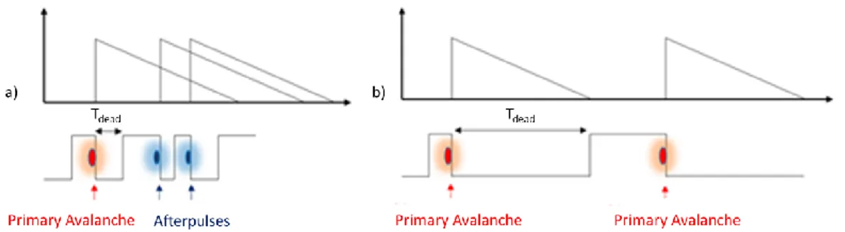
Notwithstanding the passive quenching circuit appears simple and compact, for high-rate events or for afterpulsing effects, due to de-trapping of carriers after a random time (Section 1.7.1), SPAD may create a current avalanche before the complete recharge and cause spurious carriers avalanches. Therefore, it is necessary to add a delay time, hold-off time, in the circuit design to avoid distortion in the timing response [1, 17].
The active quenching circuit is able to force the quenching and recharging process in short time and with controlled bias-voltage source [17], even if it requires much large area, at the expense of fill factor. It consists in a fast comparator to insert in
13
the circuit, whose output forces the bias voltage source below 𝑉𝐵𝐷 after the
avalanche. After an adjustable hold-off time, the bias voltage is set again to 𝑉𝑏𝑖𝑎𝑠. Basic circuits of passive and active quenching circuits are shown respectively in Fig. 1.4a, b.
Figure 1- 4. Basic circuit of SPAD with passive a) and active b) quenching circuit [13]
The active quenching circuit benefits from fast recharge, fast transitions between quenching and recharging process and shorter and controlled avalanche time and dead time [1, 7, 17].
Another solution can be the employment of a mixing active/passive circuit in order to have lower afterpulsing probability and shorter hold-off time, even if the circuit is not so compact [1].
1.4 SPAD architectures
In order to assure high level performance, SPADs require particular attention in the design and fabrication process. A highly doped region and a thin junction are required to obtain a high electric field, while a large depletion region contributes to increase the absorption efficiency [11]. In addition, in order to prevent spurious avalanches, high purity level of semiconductor, without lattice imperfections, has to be employed in SPAD design process [1]. Finally, in order to avoid premature edge breakdown (PEB) due to high doping profile curvature near the device edge, guard rings have to be insert in the structure. Guard rings avoid even spurious
14
avalanche due to carrier diffusion in the active region since they separate active region from surrounding. Sometimes so called “virtual” guard rings are employed; the term “virtual” is due to the lack of real structure in the edge of device. A “virtual” guard ring is created where the graded doping profile of the retrograde deep n-well cathode implant encourages breakdown in the central active region rather than at the device periphery [18].
According to different design, SPAD can be divided in Reach-Through avalanche photodiode, in which thick substrate constitutes the absorption region, and Planar avalanche photodiode, in which only a thin layer in the substrate is used as absorption region.
One of the first Reach-Through SPAD has been developed in the early 70s by McIntre and Webb. A Reach-Trough SPAD consists in a thin 𝑝 + doped layer, a slightly 𝑝 type doped substrate (𝜋 layer), thin 𝑝 doped layer and 𝑛 + doped layer (Fig. 1.5) [11, 19]. In 𝜋 layer the electric field is low, as shown in Fig. 1.5, while in 𝑝 − 𝑛 + junction there is a region with high electric field.
Figure 1-5. Structure of Reach-Trough SPAD [11]
When a photon hits the device, it is absorbed in the 𝜋 layer, resulting in generation of free carriers. The electric field moves the carriers towards 𝑝 − 𝑛 + junction, in which the high electric field triggers the impact ionization generating new carriers. According to different wavelength of photons to detect, the fabrication process has
15
to assure the employment of materials that guarantee photon absorption in 𝜋 layer. In this way, the device can detect photons of specific wavelengths, according to fabrication material. The guard ring of the structure is “virtual”, since, as mentioned before, it consists simply in the lack of 𝑝 implant layer near the edge of 𝑝 + layer. Additional 𝑝 dopants in 𝑝 + layer assure higher electric field in the center than in the edge region [16]. These thick devices feature high breakdown voltage, high detection probability in the visible and even in InfraRed light, large active area but poor timing resolution, due to thick junction [4].
Several types of planar SPAD have been developed since the beginning of 1970s. The thin depletion region reduces the detection probability but it improves timing performances, in timing jitter and dead time. Haitz developed one of the first planar SPAD [20]. In these devices 𝑛 + layer creates a 𝑛 + − 𝑝 junction with 𝑛-well guard ring in order to overcome the PEB problem. The multiplication layer is under 𝑛 + layer (Fig. 1.6).
Figure 1-6. Structure of planar SPAD [16]
The proximity of avalanche region to surface makes the devices sensitive to blue and UltraViolet light. This structure has been successfully integrated in Complementary Metal-Oxide-Semiconductor (CMOS) processes. In addition to planar structure with 𝑛 + − 𝑝 junction, CMOS SPADs can be developed in different configurations. If CMOS process has a deep 𝑛-well, the active region is constituted by 𝑝 + layer with 𝑝-well guard ring. The deep 𝑛-well helps to isolate the SPAD from substrate noise, since it adds another junction between 𝑛-well and 𝑝 substrate that prevents free carriers in the substrate. The 𝑛-well allows to isolate SPADs from each other and from the rest of circuitry, reducing the crosstalk probability between SPADs. The crosstalk is an unpleasant phenomenon occurring
16
when SPADs are so close that an avalanche in a SPAD causes the avalanche in neighbouring SPAD (Section 1.7.2). However, 𝑛-well isolation causes larger distances between neighbouring SPADs reducing the fill factor of the device.
1.5 CMOS SPAD technology
In the last years Complementary Metal-Oxide-Semiconductor (CMOS) technology has become the most diffused technology in digital integrated circuits for high speed, low power consumption, low fabrication costs and small area occupation. In particular, CMOS technology allows the monolithic integration of additional circuit for quenching processing and data readout and storage in the same substrate of the photodiode [21]. The integration improves the signal temporal response, reduces detector size as well as the fabrication cost. Even if CMOS technology became available in 1980s, the feasibility of CMOS SPAD has been proved only in 2003. The SPAD integration in CMOS technology requires complex processes to assure high level of performance. The fabrication material and the fabrication process have to guarantee very low level of impurities, since they could constitute energy levels in the silicon bandgap in which carriers can be trapped and after released, or in which carriers annihilate each other. Moreover, the high electric field in the depletion region should be not so high to avoid the transitions of carriers between valence and conduction bands, band-to-band tunnelling effects. The tunnelling becomes significant when electric field goes beyond 106 𝑉 𝑐𝑚⁄ [11].
However, the most important goal of SPAD in CMOS technology is to reduce the electric field in the peripheral edges to avoid premature edge breakdown (PEB). At this purpose, guard ring has to be insert in the structure. As introduced above, PEB is due to high doping profile curvature at the edge of junction, resulting in a high electric field. The key to reduce PEB probability is to reduce the electric field
17
at the edge of junction and to increase the avalanche probability in the center of multiplication region.
The first requirement against PEB consists in adding 𝑛 + layer in the central part of the junction, between 𝑛 substrate and 𝑝 surface, enhancing and confining the electric field in the central part of the junction (Fig. 1.7 a). The second option could be the insertion of low doped 𝑝 guard ring enclosing the junction, in order to decrease the electric field in peripheral edge (Fig. 1.7 b). Another solution consists in a 𝑝 diffusion close to the edge 𝑝 well at sensing area, resulting in low-doped 𝑛 region between 𝑝 area. The bias of additional gates placed on low-doped 𝑛 region causes the depletion of this region (Fig. 1.7 c).
Finally, the development of CMOS process has developed the Shallow Trench Isolation (STI) employment as guard ring. They are trenches of dielectric materials (e.g. silicon dioxide), which stop the electric current leakage in the silicon and confine the electric field (Fig. 1.7 d) [22].
Figure 1-7. a) N+ layer between n substrate and p surface, b) low doped p guard ring enclosing the junction, c) low-doped n region between p area, d) structure with STI guard ring [22]
However, STI can increase the noise level device, since they inject free carriers from STI surface to the depletion region. To reduce this level sources, implant “virtual” guard ring near STI should be designed in the device.
18
1.6 Silicon Photomultipliers
In each CMOS SPAD all electronic circuits, quenching, reset, control and read-out, are integrated in the same pixel resulting in higher time resolution and lower size and cost. Despite of these advantages, a single SPAD works as photon-trigger switch, ON or OFF state, and the output signal does not give information about the number of photons hitting the device. The signal will be the same if one or more photons simultaneously hit the device. To obtain a signal proportional to the photon flux, CMOS SPAD can be assembled in arrays. Silicon photomultipliers (SiPMs) are arrays of independent SPADs in parallel configuration with quenching resistor. Each SPAD and quenching resistor represents a cell that works independently: if a cell detects a photon triggering the avalanche, other SPADs are ready to detect another photon. This increases the photon detection capability of SPAD.
The sum of SPADs signal results in analog signal output proportional to the incident photon flux, in particular to the triggered cells and then, to the number of photons hitting the cells.
In addition to high photon detection capability, SiPMs benefit from compactness, excellent time resolution, low operative voltage. However, the analog SiPMs are susceptible to electronic noise [23] and the output signal could be altered from parasitic effects due to interconnections between SiPM and read-out electronic circuit. A buffer to isolate SPAD from the external processing electronic circuits can reduce the electronic noise effect.
The signal read-out circuit integrated in CMOS SPADs is typically constituted by a CMOS inverter used as discriminator, even if voltage comparators or source follower circuits can be found in other applications.
In addition to analog ones, SiPMs can be assembled in Digital SiPMs with each cell containing a SPAD and a more complex quenching circuit. Each cell gives an output digital signal that is successively sum up with other cells outputs.
19
Contrary to analog SiPMs, each SPAD has an own readout circuit. A digital memory is integrated in the electronic circuit to select and enable or disable SPADs in specific row and column of the array. A photon counter is connected to the cell to count the number of detected photons. This processing data configuration is known as photon counting modality.
SPAD arrays are a good solution for low light level detection applications, since it is possible to have a sensitivity down to single photon level, working in photon counting mode.
In order to have information not only about the number of detected photons, but even about the arrival time of photons, a time-to-digital converter (TDC) is co-integrated in the sensor.
In Fig. 1.8 each cell provides a fast asynchronous trigger signal and a slower synchronous data output signal. The trigger signal is connected to a balanced, low skew trigger network connected to on-chip TDC. The trigger network can be set to start the TDC at the detection of the first photon, or at higher photon threshold [23].
Figure 1-8. Scintillation light detector systems based on the analog (a) and digital (b) silicon photomultiplier [23]
Even if TDC in SPAD arrays exhibits excellent time resolution [9], it reduces the fill factor, as well as the photon detection efficiency, since it covers a large part of
20
pixel. In order to increase the FF, SPAD layout has to be put very close to read-out electronic circuit with an appropriate implant to be electrically isolated.
1.7 SPAD Noise Performance
SPAD performance is influenced to intrinsic noise sources, such as dark counts and afterpulsing events, and external noise sources due to electrical and optical crosstalk between neighbouring pixels [22].
An avalanche process can be triggered even in dark condition. The Dark Count can be constituted by avalanche pulses due thermal generation, diffusion from neutral regions, band-to-band tunnelling, trap assisted tunneling, etc. The dark counts will be deepened in the Chapter 2, while in the next paragraphs afterpulsing events and crosstalk will be explained.
1.7.1
Afterpulsing events
The impurities and crystal defects due to semiconductor material or due to fabrication process can create new energetic levels inside the bandgap of the semiconductor. These levels become trapping centers, that capture charge carriers during avalanche process. Some charges carriers can be trapped during SPAD discharge. Trapping centers are characterized by finite lifetime, i.e. the emission rate of filled traps [3], that it may vary from short time until hours. Therefore, they can be released in random time interval (Fig. 1.9). If a carrier is released when SPAD bias voltage is over the breakdown value, it can trigger another avalanche and induce a time correlated noise called afterpulse [24].
21
Figure 1-9. Mechanism of trapping and delayed realising of a free carrier by an impurity in the depletion region (afterpulsing event)
The afterpulsing probability at a time 𝑡 after the first avalanche is:
𝑃𝑎𝑝(𝑡) = 𝑁𝑐∙ 𝑃𝑡∙
𝑒−𝑡 𝜏⁄
𝜏 ∙ 𝑃𝐵𝐷 (1.9)
with 𝑁𝑐 the carriers numbers coming from the first avalanche, 𝑃𝑡 the probability that carriers remain trapped, 𝜏 the time constant of capture depending on the position of trap level inside the bandgap, 𝑃𝐵𝐷 the probability that a free carrier
generates an avalanche process. The Dark Count Rate (DCR) due to afterpulse can be evaluated as
𝐷𝐶𝑅 = 𝐷𝐶𝑅0
1 − 〈𝑃𝑎𝑝〉 (1.10)
with 𝐷𝐶𝑅0 the dark count rate without afterpulsing events [11].
Afterpulses can introduce a significant noise source (strong DCR increase), especially if afterpulse probability is so large that each pulse generates a new afterpulse. Therefore, it is important to reduce as much as possible the afterpulsing probability, 𝑃𝑎𝑝. Firstly, 𝑃𝑎𝑝 minimization can be reached by operating in design
and manufacturing process. In design process, small depletion area reduces the parasitic SPAD capacitance (𝐶𝑆𝑃𝐴𝐷), resulting in decrease of charge flowing in an avalanche:
22
𝑄 = 𝐶𝑆𝑃𝐴𝐷∙ (𝑉𝑏𝑖𝑎𝑠− 𝑉𝑏𝑑) (1.11) manufacturing process should be performed assuring high cleanness level to decrease the number of traps. Successively, during SPAD operation, it is possible to act on operating parameters, such bias voltage and temperature, to decrease afterpulse probability. If SPAD works at low bias voltage, a small number of carriers generates an avalanche. Moreover, at low voltage, the avalanche trigger probability 𝑃𝐵𝐷 will be also reduced, decreasing the probability 𝑃𝑎𝑝.
If SPAD works at low temperature, the lifetimes of traps will increase and the random release of trapped carriers will become slower, increasing the afterpulsing events at long time from the first avalanche. Working at higher temperature, SPAD afterpulse probability will decrease.
As explained in the Section 1.3.2, a circuit with large quenching resistor can be designed to introduce a dead time after photon detection in order to allow the release of all carriers. During dead time, the voltage is decrease below the breakdown value and all charges are released without any afterpulse event. Increasing the dead time, the afterpulse probability will be lower, but as well as the photon detection, since, during the dead time, the system is not able to detect photon (Fig. 1.10). By replacing a quenching transistor to a quenching resistor, the dead time can be changed modulating gate voltage in the transistor [3, 11].
Figure 1-10. Afterpulsing events introducing a short a) or long b) dead time after first carriers avalanche
23
1.7.2
Crosstalk
In addition to afterpulsing, representing a time-correlated noise source, there is a spatial correlated noise, called crosstalk, optical or electrical, between neighbouring pixels.
The optical crosstalk is triggered by emission of secondary photons from carrier avalanche (Fig. 1.11). If the photons have greater energy than the silicon bandgap, they can travel in the silicon bulk and hit directly or indirectly (optical reflection on substrate) neighbouring SPADs, triggering correlated avalanches. The crosstalk influences strongly the photon counting. SPAD output will be an incorrect evaluation of the optical signal detected by each pixel.
Crosstalk research indicated that photons triggering avalanche in adjacent pixels can be generated even by Bremsstrahlung with charged impurity centers or recombination of free charges in avalanche region [11].
Figure 1-11. Optical Crosstalk between neighbouring pixels [13]
The crosstalk probability increases with long wavelength photons, since they can cross the silicon device without being absorbed, and with SPAD density [11, 24]. Therefore, a solution to decrease the crosstalk in SiPM applications results in increasing the distance between adjacent pixels. However, this configuration would decrease the fill factor and detection efficiency. For this reason, several strategies have been employed in order to reduce crosstalk probability. Barriers with optical absorbing material between adjacent pixels can reduce the optical crosstalk, but not completely prevent it: photons can be reflected at the bottom of device bypassing
24
the barrier (Fig. 1.12). As an alternative, thick and highly doped substrates increase the absorption of secondary photons generated from carrier avalanche [25].
Figure 1-12. Direct a) and reflected b) optical path at bottom of substrate
The electrical crosstalk is due to lateral diffusion and drift of photo-generated carriers in neighbouring pixels. When multiple p-n junctions are located in the same substrate, the charge carriers can exit from depletion region and be injected in depletion region of another SPAD.
The electrical crosstalk is not influenced by temperature as afterpulse event, but it is strongly dependent on overvoltage. The charge flow in the high field region and the avalanche triggering probability are proportional to overvoltage. Working with low voltage can reduce the crosstalk probability, but even the photon detection efficiency. Another solution to decrease electrical crosstalk, as well as the optical one, consists in the isolation of pixel by STI. Exploiting dielectric material assures the electrical isolation of pixel, but influences negatively the fill factor and the photon detection efficiency. Moreover, STI can introduce defects at interface Si/SiO2 resulting in the increase of dark count rate and in DCR switching, known
25
2.Noise Sources
Introduction
The optical devices performance can be seriously compromise by level of noise, a limiting factor which impacts on the photon counting performance and detection dynamic range. The noise can be external or internal, if it is caused respectively by external factors or if it depends by internal factors.
Some noise contributions are due to:
Photon shot noise. It is due to fluctuations in the photon arrival time. The photons arrive at random intervals and the number of charges producing photocurrent is random. The fluctuations probability is governed by Poisson statistics. It is called even “white noise” because its power spectral density is constant with frequency.
Johnson or thermal noise. It is generated by thermal fluctuations in conducting materials. The electrons move in a semiconductor and they collide each other and with atoms of materials creating a current. To reduce the thermal noise, the system should be cool. Thermal noise is independent by the frequency, so it could be also considered “white noise”.
1 𝑓⁄ noise or Flicker Noise. This type of noise is present when the frequency 𝑓 is low. The mechanism that causes Flicker Noise is not clear yet. To reduce 1 𝑓⁄ noise, the detector should operate at higher frequency [1]. In addition to these signal fluctuations, dark counts in SPAD represent the main intrinsic noise source contribution. Dark counts are spurious signal pulses recorded without incident light. The noise can be uncorrelated or correlated to signal photons. The correlated noise is due to crosstalk and afterpulsing events described in the first chapter. The uncorrelated contribution can come firstly from diffusion of thermally generated minority carriers from neutral region to depletion region, or from
26
generated electron-hole pairs in depletion region due to band-to-band transition or trap-assisted transition [26, 27].
Figure 2-1. Source of noise in SPADs: a) thermal generation, b) trap-assisted thermal generation, c) band-to-band tunneling, d) trap-assisted tunneling, e) direct thermal generation and diffusion
In semiconductor material the thermal generation of carriers depends strongly on the density of local defects located in the bandgap and it increases with the temperature. These local defects depend on intrinsic material impurities or to the technological processes used in device fabrication [25]. As example, in CMOS technology STI or high doping profile can introduce a large number of defects resulting in increase of DCR. In the applications where the time of arrival of photons is unknown, the dark counts constitute an important physical background not distinguishable from the real signal.
In addition to thermal generation, the uncorrelated noise can come from trap-assisted tunnelling (TAT) or band-to-band tunnelling (BTBT) at high electric field (Fig. 2.1) [26]. SPAD bias voltage can contribute to DCR increase by means of different carriers generation mechanisms, such as Poole-Frenkel effects [28, 29] and TAT, occurring at high electric fields (> 105𝑉 𝑐𝑚⁄ ). These mechanisms can
27
generation). At higher electric field (> 7 ∙ 105𝑉 𝑐𝑚⁄ ) direct band-to-band
tunnelling (BTBT) can occur, resulting in a strong generation of free carriers in SPAD junction without the transition in deep bandgap energy levels. If the thermal carrier generation depends on temperature profile, the tunneling generation depends on electric field profile in SPAD junction. Therefore, cooling the detector can contribute to decrease thermal generation rate, but in addition an appropriate electric field profile should be designed to avoid band-to-band tunnelling and field-enhanced generation of carriers.
In addition to defects introduced during technological process, the radiation environment can introduce radiation-induced defects in silicon structure. An impinging particle can interact with silicon structure, dislodging the atom from the normal lattice site. This results in new energy levels in semiconductor bandgap, that can facilitate the transition of electrons and holes between valence band and conduction band, or that can act as trapping centres, catching carriers for a short time and releasing them later [30].
Single defects or cluster of defects may cause the switching in device current resulting in the Random Telegraph Signal (RTS) effect. In the last years different theories have been developed in order to explain the RTS. However, further investigations are necessary to clarify this phenomenon.
This chapter is focused on the main mechanisms that contribute to DCR increase and to RTS effect. RTS is deeply described in the main characteristics and in the causes that could induce it. If the dark current fluctuations between two dark discrete levels (bi-level RTS) can be easily analysed by evaluating the RTS characteristics, the analysis becomes more complicated if the fluctuations are more complex (multi-level RTS). Anyhow RTS analysis can provide tools to recognize the defect responsible for RTS, as explained in this chapter. In addition, annealing process can help in the investigation of RTS defects, since each defect anneals at specific temperature.
28
2.1 Shockley-Read-Hall thermal processes
When a thermally excited electron moves from the valence band to the conduction band leaves a hole in the valence band. This mechanism generates a charge current. Both electrons and holes contribute to charge current, so the process is known as electron-hole pair generation. The inverse mechanism is known as electron-hole pair recombination.
In silicon devices, due to large and indirect bandgap of silicon, such transitions are rare at working temperature, without extra energy [19]. However, the trap levels introduced in the bandgap by material impurities or defects can assist electron transfer and act as intermediate states between valence and conduction band. This results in a significant increase of rate of free carrier generation in darkness in semiconductor devices. This trap-assisted thermal generation is known as Shockley-Read-Hall (SRH) process [11]. The mechanisms involved (Fig. 2.2) in SRH process are:
a) electron capture: an electron transfers from conduction band to free trapped level;
b) electron emission: an electron moves from trapped level into the conduction band;
c) hole capture: an electron transfers from trapped level to a valence band, annihilating the hole;
29
Figure 2-2. Processes involved in the Shockley Read Hall model: a) electron capture, b) electron emission, c) hole capture, d) hole emission
The SRH generation/recombination rate due to trapped levels in forbidden band is
𝐺𝑆𝑅𝐻 = 𝑛𝑖 2− 𝑝𝑛 𝜏𝑒0(𝑝 + 𝑛𝑖𝑒 −(𝐸𝑡−𝐸0) 𝑘𝐵𝑇 ) + 𝜏ℎ0(𝑛 + 𝑛𝑖𝑒 (𝐸𝑡−𝐸0) 𝑘𝐵𝑇 ) (2.1)
in which 𝐺 indicates the net generation (if negative the recombination rate is higher than the generation rate), 𝑛𝑖 is the intrinsic carrier concentration, 𝑛 and 𝑝 are
non-equilibrium electron and hole concentrations, 𝐸𝑡 the trap level energy, 𝐸0 the Fermi level, 𝑘𝐵 the Boltzmann’s constant, 𝑇 the absolute temperature, 𝜏𝑒0 and 𝜏ℎ0 the lifetimes respectively of electrons and holes
𝜏𝑒0 = 1 𝑣𝑡ℎ𝜎𝑛𝑁𝑡 (2.2) 𝜏ℎ0 = 1 𝑣𝑡ℎ𝜎𝑝𝑁𝑡 (2.3)
with 𝜎𝑛 e 𝜎𝑝 are the electron and hole capture cross section, 𝑁𝑡 is the density of generation centres, 𝑣𝑡ℎ is the thermal velocity of electron and hole given by
𝑣𝑡ℎ = √3𝑘𝐵𝑇
30 with 𝑚∗ the electron or hole effective mass.
The SRH generation/recombination rate can be rewritten [3, 31]:
𝐺𝑆𝑅𝐻 = 𝑣𝑡ℎ𝜎𝑛𝜎𝑝𝑁𝑡(𝑛𝑖2− 𝑝𝑛) [𝜎𝑝(𝑝 + 𝑛𝑖𝑒 −(𝐸𝑡−𝐸0) 𝑘𝐵𝑇 ) + 𝜎 𝑛(𝑛 + 𝑛𝑖𝑒 (𝐸𝑡−𝐸0) 𝑘𝐵𝑇 )] (2.5)
If 𝐸𝑡= 𝐸0, so taking into account only those traps with energy level in the mid-gap
as generation/recombination (GR) centres, 𝐺 is maximized and it results:
𝐺𝑆𝑅𝐻 = 𝑣𝑡ℎ𝜎𝑛𝜎𝑝𝑁𝑡(𝑛𝑖
2− 𝑝𝑛)
[𝜎𝑝(𝑝 + 𝑛𝑖) + 𝜎𝑛(𝑛 + 𝑛𝑖)] (2.6) Since in the reverse-biased junction the minority carrier concentration in depletion region is lower than the equilibrium concentration (𝑝𝑛 ≪ 𝑛𝑖2), the generation process is dominant with respect to the recombination process in order to reach the equilibrium. If 𝑝 ≪ 𝑛𝑖 e 𝑛 ≪ 𝑛𝑖, the generation rate results:
𝐺𝑆𝑅𝐻 = 𝑣𝑡ℎ𝜎𝑛𝜎𝑝𝑁𝑡𝑛𝑖 [𝜎𝑝+ 𝜎𝑛]
= 𝑛𝑖
𝜏𝑔 (2.7)
where 𝜏𝑔 = 𝑣𝑡ℎ𝜎𝑛𝜎𝑝𝑁𝑡⁄[𝜎𝑝+ 𝜎𝑛] is called the generation lifetime and it describes the rate at which electron-hole pairs are generated in a depletion layer [3].
The SPAD dark count rate due to SRH generation is obtained integrating on depletion region (width 𝑊𝐷) the product of generation/recombination rate 𝐺 times
the probability for an electron-hole pair to trigger an avalanche 𝑃𝐵𝐷:
𝐷𝐶𝑅𝑆𝑅𝐻 = 𝑆 ∫ 𝐺𝑆𝑅𝐻∙
𝑊𝐷 0
𝑃𝐵𝐷(𝑧) 𝑑𝑧 (2.8)
with 𝑆 the surface of photodiode.
DCR due to thermal generation in depletion region depends on crystal defects and impurities due to fabrication process. Low DCR means a good CMOS process with
31
low defect density, while high DCR indicates high concentration of defects acting as GR centers according to SRH model.
In order to reduce DCR, it is necessary to employ devices with low impurities and, as shown Eq. 2.8, to act on design parameters such as photodiode surface (𝑆): the decreasing of size pixels reduces trap centers for trap-assisted thermal generation. Moreover, DCR caused by thermal generation depends even on working parameters such as bias voltage and temperature. Indeed, DCR increases with bias voltage since the probability to trigger an avalanche increases and the depletion region becomes larger. In addition to bias voltage, the dark count generation rate is also dependent from intrinsic concentration 𝑛𝑖 of material, depending on temperature and bandgap
energy 𝐸𝑔 [14]:
𝑛𝑖 ∝ 𝑇32∙ 𝑒− 𝐸𝑔
2𝑘𝐵𝑇 (2.9)
The bandgap of silicon is obtained by [19]
𝐸𝑔(𝑇) = 1.17 −
4.73 ∙ 10−4∙ 𝑇2
(𝑇 + 636) (2.10)
Therefore, employing a device with low intrinsic defects and working at low temperature would strongly decrease DCR [11].
2.2 Tunneling process
In order to obtain carriers avalanche, a high electric field exists in SPAD depletion region. At high electric field, the carrier generation and emission rate are increased by tunneling of electron from trap level into conduction band (Trap Assisted Tunneling, TAT) and by tunneling of electron from valence band into conduction band (Band-to-Band Tunneling). The probability of TAT is dependent on process conditions and steps introducing trap levels [19]. When electron tunnels into
32
conduction band, it leaves a hole in the valence band, therefore the tunneling process generates electron-hole pairs. TAT contribution is taken into consideration by replacing the lifetimes 𝜏𝑒0 and 𝜏ℎ0 in Eq. 2.1 with respectively 𝜏𝑒0⁄1 + Γ and
𝜏ℎ0⁄1 + Γ, where the function Γ is defined as field-effect enhancement factor [31]:
𝐺𝑆𝑅𝐻, 𝑇𝐴𝑇 = (𝑛𝑖2− 𝑝𝑛)(1 + Γ) 𝜏𝑒0(𝑝 + 𝑛𝑖𝑒 −(𝐸𝑡−𝐸0) 𝑘𝐵𝑇 ) + 𝜏ℎ0(𝑛 + 𝑛𝑖𝑒 (𝐸𝑡−𝐸0) 𝑘𝐵𝑇 ) (2.11)
The function Γ [31] is the field effect function of the TAT model, and it is expressed by Γ = 2√3𝜋|𝐸(𝑧)| 𝐹Γ 𝑒 (𝐸(𝑧)𝐹 Γ) 2 (2.12)
with 𝐸(𝑧) the local electric field intensity and
𝐹Γ =
√24𝑚∗(𝑘 𝐵𝑇)3
𝑞ℎ (2.13)
where 𝑚∗ = 0.25𝑚0 is the effective mass for tunneling (𝑚0 is the free electron rest
mass), 𝑞 is the electron charge and ℎ is the reduced Planck’s constant. The DCR caused by thermal generation (SRH model) and TAT is given by:
𝐷𝐶𝑅𝑆𝑅𝐻, 𝑇𝐴𝑇 = 𝑆 ∫ 𝐺𝑆𝑅𝐻, 𝑇𝐴𝑇∙
𝑊𝐷 0
𝑃𝐵𝐷(𝑧) 𝑑𝑧 (2.14)
The probability of tunneling is highly dependent on depletion thickness, electric field intensity and doping concentration [19]. Indeed, at high doping concentrations, the influence of TAT enhances the DCR, due to higher electric field intensity, and the strong bias voltage dependence of DCR. At low doping concentrations, the influence of TAT becomes negligible [3].
33
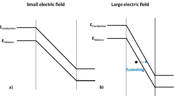
If the electric field intensity in avalanche region is very high, electrons are able to penetrate directly from valence band into conduction band through the bandgap (Band to Band Tunneling, BTBT). Contrary to TAT that occurs more frequently, BTBT is expected in extreme conditions (Fig. 2.3) [19]. The width of the bandgap is 𝐸𝑔𝑎𝑝⁄𝑞𝐸, therefore increasing electric field intensity, the width of this barrier decreases [3]. BTBT becomes the main noise source if the electric field intensity exceeds 7 ∙ 105 𝑉 𝑐𝑚⁄ [11, 31].
Figure 2-3. Tunneling probability variation in a) small electric field and b) large electric field
The generation rate due to BTBT is given by:
𝐺𝐵𝑇𝐵𝑇 = 𝐵 ∙ 𝐸(𝑧)5 2⁄ ∙ 𝐷 ∙ 𝑒
− 𝐸(𝑧)𝐹0 (2.15)
where factor 𝐵 is 4 ∙ 1014 𝑐𝑚−1 2⁄ 𝑉−5 2⁄ 𝑠−1, 𝐸(𝑧) is the electric field intensity, 𝐷 is 1 in depletion region in which tunneling effect occurs, while it is 0 on the edges of depletion region, 𝐹0 is a constant depending on the form of the potential barrier in the forbidden band. This value is important since it determines the temperature dependence of the tunneling current. In literature it is given by 1.9 ∙ 107 𝑉 𝑐𝑚−1
34
[3]. Moreover, BTBT is strongly dependent on electric field intensity and on doping profile: with high doping profile, the depletion region is thinner and BTBT probability increases.
The dark count rate due to tunneling is
𝐷𝐶𝑅𝐵𝑇𝐵𝑇 = 𝑆 ∫ 𝐺𝐵𝑇𝐵𝑇∙
𝑊𝐷 0
𝑃𝐵𝐷(𝑧) 𝑑𝑧 (2.16)
The total DCR is given by all three contributions [31]:
𝐷𝐶𝑅𝑇𝑂𝑇 = 𝐷𝐶𝑅𝑆𝑅𝐻+ 𝐷𝐶𝑅𝑇𝐴𝑇+ 𝐷𝐶𝑅𝐵𝑇𝐵𝑇 (2.17)
2.3 Poole-Frenkel effect
Depending on the electric field, it could be necessary take into account in Dark Count the contribution due to Poole-Frenkel (PF) effect [28, 29]. This effect becomes dominant at moderate electric fields (104 𝑉 𝑐𝑚⁄ ) [32].
The Poole-Frenkel effect is an electric-field-induced lowering of potential barrier for the thermal emission of a carrier from a level in the bandgap (Fig. 2.4) [33].
![Figure 1-1. Absorption coefficient as a function of incident light wavelength for semiconductor material [11]](https://thumb-eu.123doks.com/thumbv2/123dokorg/2872626.9530/18.892.300.623.464.777/figure-absorption-coefficient-function-incident-wavelength-semiconductor-material.webp)
![Figure 1-2. a) Current-voltage characteristic; b) Description of working processes in SPAD [1]](https://thumb-eu.123doks.com/thumbv2/123dokorg/2872626.9530/20.892.176.778.631.794/figure-current-voltage-characteristic-description-working-processes-spad.webp)
![Figure 2-7. NIEL as a function of energy for electrons, pions, neutrons and protons [42]](https://thumb-eu.123doks.com/thumbv2/123dokorg/2872626.9530/56.892.235.726.171.505/figure-niel-function-energy-electrons-pions-neutrons-protons.webp)
![Table 2-2. Energy levels in eV of some defect states. The subscript c stands for conduction and v for valence [65]](https://thumb-eu.123doks.com/thumbv2/123dokorg/2872626.9530/72.892.212.719.168.527/table-energy-levels-defect-states-subscript-conduction-valence.webp)
![Figure 2-14. Schematic representation of intercenter transfer mechanism with diagram of SRH generation [71]](https://thumb-eu.123doks.com/thumbv2/123dokorg/2872626.9530/75.892.303.639.290.619/figure-schematic-representation-intercenter-transfer-mechanism-diagram-generation.webp)
![Figure 3-6. a) Cross section of PN layout; b) Cross section of PWNISO layout [76]](https://thumb-eu.123doks.com/thumbv2/123dokorg/2872626.9530/83.892.181.757.289.477/figure-cross-section-layout-cross-section-pwniso-layout.webp)