A 11-15 GHz CMOS
÷2 FREQUENCY DIVIDER
FOR BROAD-BAND I/Q GENERATION
Annamaria Tedesco, Andrea Bonfanti, Luigi Panseri, Andrea Lacaita
Dipartimento di Elettronica ed Informazione - Politecnico di Milano,
P.za Leonardo da Vinci 32, I-20133 Milano, Italy
E-mail:
[email protected]
ABSTRACT
This paper presents a 0.13 µm CMOS frequency divider
for I/Q generation. To achieve a wide locking range, a novel topology based on a two stages injection-locking ring oscillator is adopted. This architecture can reach a larger input frequency range and better phase accuracy with respect to injection-locking LC oscillators, because of the smoother slope of its phase-frequency plot. Post layout simulations show that the circuit is able to divide an input signal spanning from 6 to 24 GHz, although the available tuning range of the signal source (integrated VCO) limited the experimental verification to the interval 11-15 GHz, with a consequent measured 31% locking range. A single divider dissipates 3 mA from 1.2 V power supply.
1. INTRODUCTION
High-speed frequency dividers are among the most critical building blocks in modern CMOS wireless tranceivers. They are employed both in the feedback path of Phase Locked Loops (PLL) and to generate the I/Q quadrature signals necessary in zero- or low-IF receivers. The design of a fully integrated CMOS divider is critical, above all for its power consumption that is comparable to the one of the Voltage Controlled Oscillator (VCO). This problem becomes even more severe when a wide input frequency range is required, since in this case it is not possible to adopt resonant loads, that would allow power reduction. Moreover, the dissipation of a broad-band buffer, usually interposed between the VCO and the divider itself, must be also taken in to account in the total power budget. We
discuss a topology for a ÷2 frequency divider for I/Q
generation in a WLAN transceiver for IEEE 802.11a/b/g standards. In the frequency synthesizer only one VCO will be employed, and a first divider provides the I/Q signals for the 802.11a channels without using an input buffer. Then, a following divider makes the signals for the 2.5 GHz band available. The key advantage of this architecture is that VCO pulling is avoided. Given the channellizations of the standards, the input frequency of the first divider must vary between 9.6 and 11.6 GHz, leading to 18 % input tuning, or locking, range. However, a more conservative figure for the locking range is 35%, to account for the process spreads in the VCO. In the next section we will recall why such high tuning range makes not possible to adopt some recently presented low-power
solutions, as LC injection locking topology. Then we discuss the circuit topology and we show why this circuit can achieve a wide tuning range. We present the circuit implementation, some experimental results and, then, the conclusions will follow.
2. HIGH-SPEED DIVIDERS
High-speed dividers are typically realized as two latches in a negative feedback loop [1]. For multi-GHz input signals, these circuits have a differential current-steering structure that allows fast current switching, usually called source-coupled logic (SCL). To reduce the dissipation a dynamic logic was employed in [2], but it does not provide I/Q outputs. Probably, the best solution in term of power consumption is to differentially drive two injection locking LC oscillators, as in [3]. With respect to the SCL dividers the dissipation reduces by about Q, the quality factor of the divider’s resonant tank, at the cost of a large area occupation. Unfortunately, this topology is intrinsically narrow band: to increase the divider locking range the quality factor Q of the LC tanks must be lowered with a resulting rise in dissipation. Our locking range requirements demand a low Q, close to two, practically voiding the effect of the LC resonance. In this sense, power is traded not only with speed, but also with input locking range. A further example of this trend is the 40 GHz divider presented in [4], which demonstrates good power performance but features 6 % locking range.
2.1 Proposed injection-lock ring divider
Our approach was to injection-lock a wide tuning range oscillator, namely a two-stages ring oscillator. Self oscillating dividers have also the useful property of requiring less power from the driving signal, avoiding the use of a power consuming buffer. Fig.1 shows the circuit scheme and the detail of one stage. Simulations show that the transfer function of the single stage can be approximated as:
( )
z 0 p 1 j T j T 1 j − ω ω ω = + ω ω (1)The small signal dc gain is T0 = gmiR/(1 – gmcR), being gmI
-M4 respectively. The dominant pole frequency is ωP=(1–
gmcR)/COR, where CO is the output load capacitance.
Owing to the gate-drain overlap capacitance of the input
couple M1-M2, the transfer function also exhibits a right
half-plane zero at higher frequency, ωZ = gmi/Cgd To satisfy
the Barkhausen criterion for loop phase, a lag of – π/2
radians is required for each stage, providing in this way the quadrature outputs. The cross-connection between the
two stages in Fig.1 gives the remaining phase shift of π.
The – π/2 delay is reached only thanks to the right zero,
and it is straightforward from (1) to evaluate that this shift is achieved at a frequency corresponding to the geometric mean between the pole and the zero. The ring oscillation
frequency is thus ω0 = (ωp ωz)1/2. Using (1) and the
Barkhausen criterion for loop magnitude, we obtain the condition for the dc gain: T0(ωp /ωz)1/2 = 1. Then, when
the amplitude rises, the “effective” transconductance of
the cross-coupled pair M3-M4 reduces with respect to the
initial small signal value gmc/2, until the oscillation
becomes stable. It’s important to note, from the expression
of the dominant pole frequency, that also ωP and,
accordingly, ω0 vary. Both ωP and ω0 increase when the
transconductance of the pair M3-M4 lowers. In an
oscillator this effect would lead to very poor performance in term of frequency stability and phase noise. In our application we do not face this problem, since the circuit is driven by an input signal.
A similar analysis can be found in [5], though the circuit in that case is a standard SCL divider, and only simulation results are shown. In our case the cross-coupled pair acts as a gain-boosting stage at the start-up and then as an amplitude limiter to stabilize the oscillation, and not as a latch for data holding. An injection-locking ring is also discussed in [6]. In that paper however, the circuit only generates the I/Q signals without dividing the VCO output, that could suffer from pulling effect.
2.2 Lock Range and Phase Accuracy
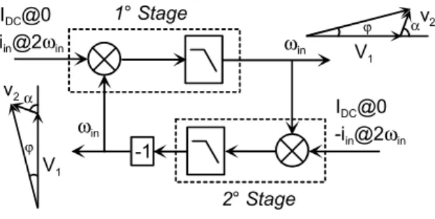
The two differential outputs of the VCO, running at 2ωin,
drive the divider through the tail transistors of the two
stages, M5 in Fig. 1 and the analogous one of the other
stage. In this way the injected current iin, at 2ωin is
superimposed to the dc tail bias current IDC. In this way the
ring is forced to oscillate at ωin, which is in general
different from ω0. The mechanism of injection locking has
been rigorously discussed by many authors, see for instance [3], [6], [7] and is intuitively recalled with the help of Fig. 2.
A steady condition is reached when the ring oscillates at ωin. In this case the input pair M1-M2 in Fig. 1 behaves as a
mixer for the signal coming from the tail and thus converts IDC and iin to ωin. The dominant pole of each stage
filters out the higher-frequency products. Since ωin differs
from ω0, the lag of each stage is not exactly –π/2 but it is –
π/2–ϕ. The mixer stage must balance this phase shift ϕ adding the opposite shift to its output. That is sketched in Fig. 2, where all the represented phasors rotate at ωin. V1
represents the output signal as a result of the dc current,
while v2 is the additional signal caused by the injected
current. The loop adjusts the phasors, by settling the angle α, in order to obtain an additional shift ϕ, with respect to the state in which there’s not injection of current. It is easy to see that when a differential signal, iin and –iin, is forced in the two stages, their outputs are still in quadrature. It is also possible to evaluate which is the the maximum
frequency deviation, ∆ω, from ω0 so that the divider can
properly operate, [7]. If we call SL the magnitude of the
slope, evaluated at ω0, of the phase vs. frequency
characteristic of T(jω), it results SL ≅ ϕ/∆ω. If we define
the injection strength m = v2/V1 = iin/IDC, Fig.2 shows that,
with a good approximation, is ϕmax≅ m, and consequently
∆ωmax≅ m/SL. Consequently the lock range increases with
m, and it is also inversely proportional to SL. From equation (1) it is possible to simply evaluate the magnitude of the slope. Recalling that the expression for the free running frequency, ω0, is ω0 = (ωP ωZ)1/2, it
results:
(
)
0 p z d SL 2 d ω ϕ = = ω + ω ω (2)For a given ω0, this value is much smaller than the
corresponding one in an LC tank oscillator, namely 2Q/ω0.
In fact, first, the arithmetic mean (ωp + ωz)/2 is always
larger than the geometric mean, ω0. Second, the factor 2Q
ωin I 180° + _ 2ωin Q 0° + _ ωin V DD gmi gmc 2ωin
+
_
_
+
R Vbias M1 M2 M5 M4 M3 RFigure 1. Ring frequency divider driven by a
differential VCO. The scheme of one stage is also
ωin IDC@0 iin@2ωin -1 IDC@0 -iin@2ωin ωin 1° Stage 2° Stage ϕ αv2 V1 ϕ α v2 V1
Figure 2. The injection locking mechanism in
is usually greater than one. Thus, the lock range obtained is accordingly larger. Moreover a low value of SL provides also benefits to the quadrature accuracy. The quadrature error is due to the mismatch between the values
of ω0 in the two stages. For a difference dω0, a
corresponding variation dϕ must thus occur. That can be
achieved only by changing the angle α between the
vectors V1 and v2. This shift dα, is the quadrature error.
From the phasors diagram in Fig.2 we obtain that:
(
)
2 1 m 2mcos d d m m cos + + α α = ϕ + α (3)Since the magnitude of dϕ is approximately |dϕ| ≅ SL
|dω0|, also in this case a smoother slope SL is beneficial.
3. CIRCUIT REALIZATION
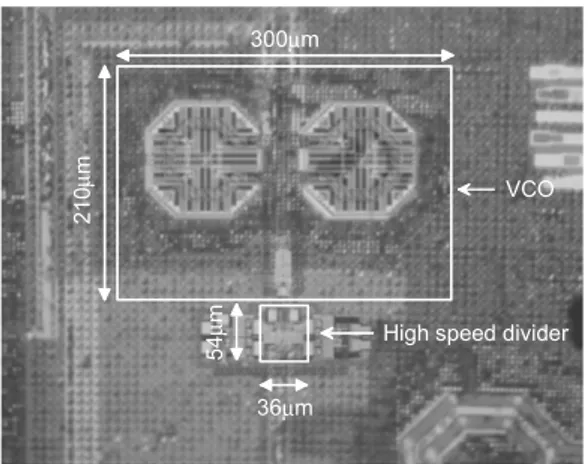
A cascade of two dividers has been integrated in a STM
0.13µm CMOS technology. A differential VCO as signal
source and a quadrature mixer are integrated on the same die. The two circuits have the same topology, with the difference that in the second divider the bias current is almost half of the first divider, because of its halved operating frequency. Fig. 3 shows a photo of the chip. The inductors of a differential LC-tank VCO fill most of the area. The only signals available are the ones at the output of the VCO and of the second divider. Moreover in order to let the first circuit oscillate in free running mode, it is possible to switch-off the power supply of the VCO. Post-layout simulations show that the first circuit can operate with an input frequency varying between 6 and 24 GHz. Fig. 4 shows the simulated sensitivity curve between the minimum amplitude of the input signal of the first divider and its operating frequency. At 19 GHz the amplitude of the voltage signal at the input of the divider is zero. This means that the divider operates in free running mode.
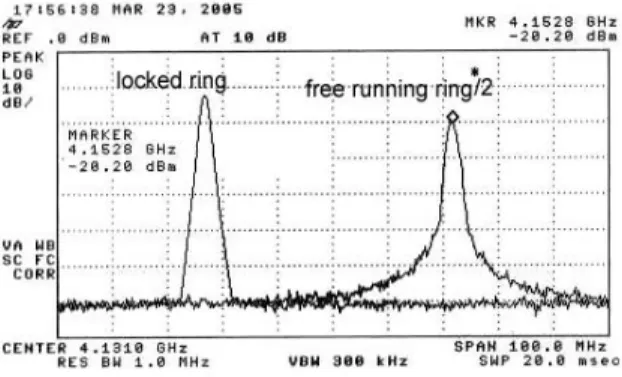
4. EXPERIMENTAL RESULTS
As previously discussed, one characteristic of these dividers is the capability to operate both driven by an input signal and in free running mode For comparison, two measured output spectra are superimposed in Fig. 5. The spectrum on the left side was measured when the divider chain is driven by the VCO. Its center frequency,
shifted in the figure for comparison, is 3.66 GHz,
corresponding to a VCO frequency four times higher, that is 14.64 GHz. The spectrum on the right side is the one of the first ring operating in free running mode, divided by two by the second ring. The measured locking range is close to 31 % because it was possible to test the divider chain only at the operating frequencies of the VCO, between 11 and 15 GHz. The measured free running frequency is 8.3 GHz, a value slightly inferior to the one obtained by simulations. Actually, the divider current needed for free-running oscillation was slightly higher than the one used in the simulations. This may be due to the underestimation of the parasitic capacitances which leads to a lower open-loop gain.
Fig. 6 shows first the output phase noise when the VCO is switched off. It is the phase noise of the first ring, reduced of – 6 dB by the frequency division. As expected, this noise is very high, but it does not impair the overall noise performance. When the two dividers are injection-locked to the VCO it is the phase noise of this circuit that appears at the output. In Fig.6 in fact, we also compare the measured phase noise of the VCO with the one at the output of the two locked dividers. The frequency division by four reduces the noise by 12-dB and confirms that the ring phase noise doesn’t affect the output phase noise. In Table I are summarized the two dividers’ performances.
5. CONCLUSIONS
A novel topology of frequency divider has been presented. The key feature of the circuit is the reduced slope of the phase-frequency plot of one single stage. That allows
6 8 10 12 14 16 18 20 22 24 0.0 0.2 0.4 0.6 0.8 1.0 1.2
In
put Vol
tage
[V
]
Input Frequency [GHz]
Figure 4. Simulated sensitivity curve between
the minimum amplitude of the input signal of the first divider and its operating frequency.
300µm 36µm 21 0µ m 54 µ m VCO
High speed divider
achieving a measured locking range about 31% of the center frequency, with a reasonable power budget. This value is limited by the operating frequency range of the VCO (11-15 GHz) used as injection signal. Simulation demonstrate even a larger locking range, 6 – 24 GHz, which was not possible to experimentally verify given the limited tuning range of the signal source.
6. REFERENCES
[1] B. Razavi, RF Microelectronics, Prentice Hall, Upper Saddle River, NJ, USA, 1998, pp. 290-295.
[2] S. Pellerano, S. Levantino, C. Samori, and A. Lacaita, “A 13.5-mW frequency synthesizer with dynamic-logic frequency divider,” IEEE Journal of
Solid-State Circuits, vol. 39, pp. 378-383, Feb. 2004. [3] A. Mazzanti, P. Uggetti, and F. Svelto, “Analysis and
design of injection-locked LC dividers for quadrature
generation,” in IEEE Journal of Solid-State Circuits, vol. 39, pp. 1425-1433, Sept. 2004.
[4] J. Lee, and B. Razavi, “A 40-GHz frequency divider
in 0.18 µm CMOS technology,” in IEEE Journal of
Solid-State Circuits, vol. 39, pp. 594-601, April 2004. [5] R. Dehgahani, and S. M. Atarodi, “A low power
wideband 2.6 GHz CMOS injection-locked ring oscillator prescaler,” in Proc. RFIC Symposium, pp. 659-662, Philadelphia, PA, 8-10 June 2003.
[6] P. Kinget, R. Melville, D.Long and V. Gopinathan, “An injection-locking scheme for precision quadrature generation,” IEEE Journal of Solid-State
Circuits, vol. 37, pp. 845-851, July 2002.
[7] R. Adler, “A study of locking phenomena in oscillators,” Proc. IEEE, vol. 61, pp. 1380-1385, Oct. 1973.
Figure 5. Output spectrum (left) of the cascade
of the two dividers driven by the VCO running at 14.64 GHz (the spectrum is shifted for sake of comparison), compared with the spectrum (right) of the first ring in free running, divided by two.
Table. 1. Measured Dividers Performance
Power supply 1.2 V
Bias current – first divider 3 mA
Bias current – second divider 1.5 mA
Free running frequency – first divider. Free running frequency – second divider
8.3 GHz 5.5 GHz
Input frequency range 11 – 15 GHz
10k 100k 1M 10M -150 -140 -130 -120 -110 -100 -90 -80 -70 -60 -50 -40 -30 -20 -10 VCO locked ring
free running ring /2
P h a se N o ise [d B c /H z] Frequency Offset [Hz]
Figure 6. Comparison between the phase noise of
the VCO and the phase noise at the output of the two dividers. The difference is 12 dB, indicating that the dividers do not impair the noise performance.