ScienceDirect
Energy Procedia 00 (2015) 000–000
www.elsevier.com/locate/procedia
1876-6102 © 2015 The Authors. Published by Elsevier Ltd.
Peer-review under responsibility of The European Materials Research Society (E-MRS).
E-MRS Spring Meeting 2015 Symposium C - Advanced inorganic materials and structures for
photovoltaics
Analysis by finite element calculations of light scattering in
laser-textured AZO films for PV thin-film solar cells
D. Canteli
a, J. M. López
a, S. Lauzurica
a, M. Lluscà
b, M. I. Sánchez-Aniorte
a, J.
Bertomeu
b, M. Morales
a, C. Molpeceres
aaCentro Láser, Universidad Politécnica de Madrid, Carretera de Valencia km 7,3, Madrid 28031, Spain bDepartment of Applied Physics and Optics, Universitat de Barcelona, Av. Diagonal 645, Barcelona 08028, Spain.
Abstract
In the thin-film photovoltaic industry, to achieve a high light scattering in one or more of the cell interfaces is one of the strategies that allow an enhancement of light absorption inside the cell and, therefore, a better device behavior and efficiency. Although chemical etching is the standard method to texture surfaces for that scattering improvement, laser light has shown as a new way for texturizing different materials, maintaining a good control of the final topography with a unique, clean, and quite precise process.
In this work AZO films with different texture parameters are fabricated. The typical parameters used to characterize them, as the root mean square roughness or the haze factor, are discussed and, for deeper understanding of the scattering mechanisms, the light behavior in the films is simulated using a finite element method code. This method gives information about the light intensity in each point of the system, allowing the precise characterization of the scattering behavior near the film surface, and it can be used as well to calculate a simulated haze factor that can be compared with experimental measurements. A discussion of the validation of the numerical code, based in a comprehensive comparison with experimental data is included.
© 2015 The Authors. Published by Elsevier Ltd.
Peer-review under responsibility of The European Materials Research Society (E-MRS).
Keywords: Laser texturing; light management;finite element method (FEM) simulations.
1. Introduction
A strategy to improve the solar cells efficiency is to have one or more textured surfaces inside the device that produce a high light scattering in the wavelength range from 500 nm to 1000 nm, increasing the light path in the absorptive layer, and so, allowing a higher absorption [1]. There are two typical ways to obtain a textured surface:
approximate value of the electromagnetic field at every point of a system, and could be used over theoretical surfaces, making easy the study of the effect of different morphologies over the film or device properties.
This work shows the comparison between experimental and simulated haze factors for several laser-textured AZO films, and discusses the different parameters used to characterize this kind of surfaces, as well as the light distribution observed near the textured surfaces. To calculate the scattered light in laser-textured AZO films the finite element method (FEM) has been used, which deals with the electromagnetic scattering problem by discretizing Helmholtz equation in space, solving it numerically as a boundary value problem [7], and it has been previously used to study light scattering [1, 8].
2. Experimental
2.1. TCOs samples preparation
The films used were aluminum-doped zinc oxide (AZO) thin-films deposited by direct current (DC) magnetron sputtering onto 10 × 10 cm2 Corning 1737F glass substrates, using a power of 200 W, an argon working pressure of
0.4 Pa, and maintaining a substrate temperature of 300 ºC during the deposition [9]. The as-deposited AZO films presented an average transmittance of 80% in the 400-800 nm range, and a sheet resistance of 7 Ω/sq. The thickness of the films was about 1000 nm and had a smooth surface, with root mean square roughness, σrms, about 7 nm.
2.2. Laser systems
The AZO films were textured using a diode-pumped solid-state laser (Nd:YVO4) from Spectra Physics working
at the third harmonic wavelength, 355 nm. This source emits pulses about 10 ns of duration, and the laser beam radius on focus is 17 µm. To generate a texture in the films, successive parallel grooves were ablated in the film maintaining a constant separation between grooves. Although different process parameters (laser average power, process speed and groove distance) were tried, as well as the use of one or more arrays of grooves with different directions (more details about those samples are given by Lauzurica et al. [4]), in this work we focus in the parallel grooves scheme with just one array of processes, showed in the image on the left in Fig 1. The four samples used in this study were textured at 50 kHz and scan speed of 85 mm/s, with a distance between grooves of 10 µm or 20 µm and average laser power ranging between 75mW and 135 mW. The process parameters and most relevant properties of the samples studied are listed in table 1.
Table 1. Process parameters (laser power and distance between laser processes) used to texture the AZO films, and properties of the textured samples. In the four samples the repetition frequency was 50 kHz and the process speed was 85 mm/s.
Sample Laser parameters Average T (400-800 nm) (%) Haze Factor (600 nm) (%) σrms (nm) Sheet resistance (Ω/sq)
A 75 mW, 10 µm 77.8 12.7 76 11
B 100 mW, 10 µm 81.9 18.6 151 60
C 100 mW, 20 µm 78.5 11.7 183 12
D 135 mW, 20 µm 81.5 37.1 284 110
Fig. 1. (a) Diagram of laser texturization process of AZO thin-films used in this work; (b) Scheme of the FEM model used to simulate scattering at the laser-textured AZO films. In the model a Gaussian beam of light, incident from the left, passes through the AZO film and is scattered in the AZO-air interface, traveling to the semicircular edge of the domain where the far field is calculated.
2.3. Characterization techniques
The textured films were morphologically characterized using a confocal microscope Leica SensoScan, from which the 3D images, profiles, and σrms values were obtained. The optical properties of the samples such as total
transmittance (Tt) and diffused transmittance (Td) were measured with a PerkinElmer Lambda 950 spectrophotometer equipped with a 150 mm integrating sphere. To evaluate the scattering of light in the laser-textured samples, the haze factor values were calculated using the following expression: Haze Factor = 100·Td/Tt. The sheet resistance (Rs) of the samples was measured with a four-point probe system (Jandel RM3). Due to the
directional morphology of the textured samples, the Rs values shown in table 1 are average values of several
measures made in two positions, with the probes in two orthogonal directions.
3. Simulation model
3.1. FEM model description
A COMSOL simulation software version 4.4 with a radio frequency (RF) module was used to construct the simulation system. When working with electromagnetic field calculations, the size of the model elements must be at least five times smaller than the light wavelength [1, 8]. With a wavelength of 500 nm, for example, this condition means ~3·104 nodes/µm3, or ~300 nodes/µm2 when working in a 2D model. This limits the size of the model,
because the larger number of nodes, the higher number of calculations must be done. Although this study aimed to calculate scattering in sample areas of tens of microns, that kind of simulation in a 3D system would suppose a very high number of nodes and a huge calculation capacity. Due to the limited capacity of the work station used, it was decided to take advantage of the sample properties and use the 2D model shown in the right image on Fig. 1, formed by a semicircular domain with a radius of tens of microns (maximum 100 µm). In this model, similar to the experimental system used to measure the total and diffuse transmittances of the film, the light enters the system from the left, passes through the AZO film, and is scattered at its surface. The scattered waves travel towards the circular edge where the far-field intensity is calculated.
If a planar incident wave of light is used for the simulation part of the light will produce reflections in the points where the surface met the semicircle. To avert these unwanted reflections a Gaussian beam, according to equation 1 was selected instead of a planar wave.
2 2 0 0
y
E E e
=
⋅
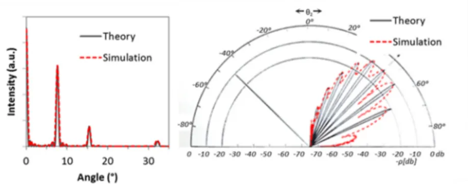
− ω (1)Fig. 2. Theoretical calculations (continuous black line) and simulation results (dashed red line) for a diffraction grating of nine slits of 2.5 µm wide separated 7.5 µm one to another (left), and for the reflection of a light beam incident at 45º into a sinusoidal surface (right). The theoretical results for the right image have been taken from [12].
To avoid dispersion of the Gaussian beam, related to the ratio between the beam width and the wavelength, the beam width must be more than five times the light wavelength [1]. A beam width ω0 equal to 0.6 of the domain
radius was used, which it is about 30 µm, so the calculations are not influenced by the beam dispersion.
Refractive index values of the AZO films used were obtained from literature [10]. Taking samples profiles obtained with the confocal microscopy, the angular resolved scattering (ARS) of the four samples was computed from far-field calculations. Finally, by choosing an angle to differentiate between specular and diffuse fractions of light, the haze factor is calculated from the ARS results, and compared with the experimental data. An angle of 6°, similar to the one in the integration sphere (measured from the center of the sample port, where the textured sample is placed, to the edges of the opening allowing the exit of specular light), was chosen.
3.2. Verification of the model
The model was tested comparing the theoretical and calculated ARS of two different systems. First an ideal diffraction grating formed by nine slits of 2.5 µm wide in a metallic film separated 7.5 µm from one another was studied. The angular scattering produced by that grating could be easily calculated from equation 2.
( )
( )
( )
( )
( )
0 2 2 sin sin sin sin sin sin sin sin b d N N I I b dπ
θ
π
θ
λ
λ
θ
π
θ
π
θ
λ
λ
⋅ ⋅ ⋅ ⋅ = ⋅ ⋅ ⋅ ⋅⎛
⎛
⎞
⎞ ⎛
⎛
⎞
⎞
⎜
⎟
⎜
⎟
⎜
⎝
⎠
⎟ ⎜
⎝
⎠
⎟
⎜
⎟ ⎜
⎟
⎛
⎞
⎛
⎞
⎜
⎟ ⎜
⎟
⎜
⎟
⎜
⎟
⎜
⎝
⎠
⎟ ⎜
⎝
⎠
⎟
⎝
⎠ ⎝
⎠
(2)The second system was the reflection of incident light at 45º on a sinusoidal surface given by the expression: y(x) = h·sin(K·x), with K·h = 1 and a period Λ = 10·λ, being λ the wavelength of the incident light. The calculations of scattered intensity for this case are quite complicated [11, 12]. In Fig. 2 the ARS obtained with the theoretical calculations is presented with a continuous black line and the results obtained using the model with a dashed red line. The theoretical diagram showed for the sinusoidal surface reflection was taken from the study of P. Beckmann et al. [12]. As it can be seen, both cases show very good agreement between theoretical and simulated results.
4. Results and discussion
4.1. Laser texturing results
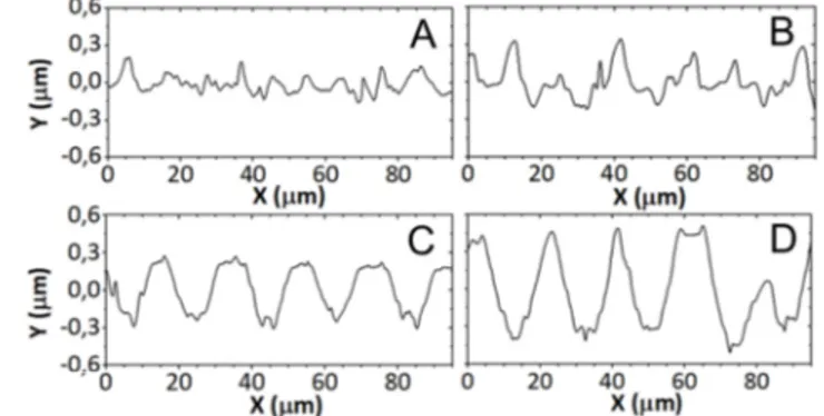
The laser texturing processes were performed at 355 nm and 50 kHz, with a process speed of 85 mm/s and different values of laser power and groove separation. Fig. 3 shows profiles of the four laser-textured AZO films studied in this work, measured in a perpendicular direction to the grooves.
Fig. 3. Profiles of the four samples studied in this work, obtained by confocal microscopy. Process parameters and properties of the samples are listed in table 1.
The textured samples maintain good optoelectronic properties, similar to the as-deposited film, with an integrated transparency in the 400-800 nm range over 75 %, and a sheet resistance ranging between 11 Ω/sq and 110 Ω/sq, presenting in addition quite interesting haze factor values (see Fig. 4). The high σrms values of the samples, ranging
between 70 and 290 nm, can be misleading, as the σrms roughness gives a measurement of the height variations of the
surface, but does not consider its lateral proportions. The process parameters, as well as the most relevant properties of the textured films are listed in table 1.
4.2. FEM model results
As has been said before, from profiles of the laser-textured films measured by confocal microscope it is possible to simulate the ARS of the different samples. And by selecting an angle to distinguish between diffuse and specular light, the haze factor of each sample can be calculated. Fig. 4 shows the comparison between the experimental haze measurements and the simulated results for the four samples. The solid lines show total transmittance (red line) and haze factor (blue line) of the samples, and the dashed lines are the simulated values obtained with the FEM model using a 6º angle to discriminate between specular and diffuse light.
The results are in good agreement with experimental data. However, there are some discrepancies: at λ < 650 nm the simulated haze factor is smaller, and at λ > 1100 nm both the haze factor and the total transmittance overestimate the experimental values. The main reason for these discrepancies could be the mismatch between the AZO refractive index used and the real one. There are also aspects of the simulations and the experimental measurements which influence on the results is hard to evaluate. Firstly, the use of a 2D profile instead of a 3D surface: in the 2D profile the angle between the forms with the normal to the substrate are always lower than in the 3D surface, so a 3D surface would increase the diffused transmittance, and also the haze. Secondly, the AZO refractive index can suffer changes during the laser process (for example by crystallization of the film). Finally, when using an integrating sphere, due to the finite size of the port used to remove the specular light, part of the scattered light falls into that port and is counted as specular light [6]. Also the influence of the illuminated area in the haze results is difficult to assess.
Where n0 and n1 are the refractive index of the two materials (in this case air and TCO), and
γ
and Ccorr(λ) aretwo fitting parameters, initially fixed at 2 and 1, respectively. This theory is used in several works to study random textured surfaces [13-16], but trying to use it with the laser-textured AZO samples of this work leads nowhere, because eq. 3 is valid under two assumptions: the surface must have a random surface roughness with a Gaussian height distribution, and its correlation length (that gives a measure of the average roughness lateral size) should be much larger than the wavelength of light [14].
In the samples showed in this work, where the surface morphology has some kind of ordered structure, other scattering source appears: the interference of light from different parts of the sample becomes critical. In particular, the grooves of the AZO samples studied in this work act as slits of a diffraction grating, producing a scattering behavior very similar to that of a diffraction grating. This can be seen if the laser-textured surfaces are illuminated with a low intensity laser beam, appearing several intensity maxima at regular distances.
Olindo et al. [15] suggested that the scattering produced in a surface is achieved by superposition of different scattering mechanisms caused by the different geometrical features integrated in a modulated surface texture. With this in mind, the laser-textured samples discussed here will look like a sinusoidal surface with some roughness on it, so there will be two different scattering sources.
Fig. 4. Experimental measurements (solid lines) and simulation results (dashed lines) for hemispherical transmittance (red) and haze factor (blue) of the four samples. A 6º angle, similar to the angle in the experimental measurements, has been used in the simulation model to discriminate between specular and diffuse light.
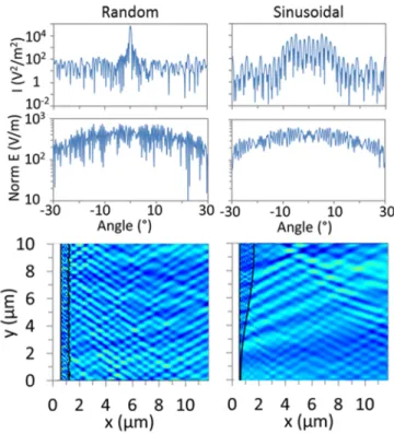
Fig. 5. Angle resolved scattering obtained from far-field calculations (top), normalized electric field measured at one micron from the surface (middle) and detail of the normalized electric field distribution near the film surface (bottom) for a random textured surface (left) and a sinusoidal surface (right). The sinusoidal surface has a period of 20µm, and a size of 60 µm. Both images are in the same scale, dark blue used for lower electric field intensities and bright blue for higher intensities.
To have a deeper knowledge of the scattering scheme of both contributions, the scattered light by a random-textured and a sinusoidal surface was simulated. The random surface used is a smooth function that connects points with a normal distribution of heights and a 50 nm of average value, at a distance of 50 nm from each other, while the sinusoidal surface is similar to the laser textured films, with a period of several microns and amplitude of 0.5 µm. The upper images in Fig. 5 show the ARS of both surfaces, being these very different, with a main intensity peak of specular transmitted light in the random-textured case, meanwhile the ARS of the sinusoidal surface shows a pattern of several maxima of similar intensities due to diffraction. This could lead to errors when studying ordered surfaces, especially in the haze calculations when it has to separate the specular and the diffuse light and should be taken into account when measuring the haze factor of surfaces with an ordered texture.
Anyhow, close to the surface of the film (the region of interest for thin film devices), simulations show that the electric field distribution (as well as the light intensity) is quite similar in a film with a random surface or in a sinusoidal surface, as it can be seen from the middle and lower images in Fig.5.
In the region of one or two microns closer to the surface, which is the characteristic thickness of thin-film devices, maxima and minima of the electric field due to constructive and destructive interference of light are present. In that region the scattering generated in a sinusoidal surface is similar to that obtained with a random surface roughness, even though the former one has a much greater period than the light wavelength. This would lead to an improvement in the optical behavior of thin-film cells due to a higher absorption of light.
5. Conclusions
Four AZO films have been textured with a pattern of parallel laser processes using nanosecond laser pulses at 355 nm. The textured films show a high haze factor maintaining a good transmittance and low sheet resistance. Unlike random-textured surfaces, the laser-textured samples show several maxima of intensity when illuminated with a laser
of any surface, random or ordered, theoretical or experimental. Taking advantage of that, a brief study of the scattering close to the TCO surface, for both a random-textured and an ordered film, has been carried out showing that the light intensity distribution in both cases is quite similar in that region. This suggests that the laser-textured films will produce an increase of light absorption in thin-film solar cells, but to ensure that the films should be tested in device.
Acknowledgements
This work has been supported by the Spanish Ministerio de Economía y Competitividad and the European Regional Development Fund through the project HELLO (ENE2013-48629-C4-2-R and ENE2013-48629-C4-3-R).
References
[1] Čampa A, Topič M. Calculating haze parameter of textured transparent conductive oxides. In Proceedings of the 2012 COMSOL Conference, 2012; 6.
[2] Remes Z, Vanecek M, Yates HM, Evans P, Sheel DW. Optical properties of SnO2:F films deposited by atmospheric pressure CVD. Thin Solid Films 2009; 517; 6287-3.
[3] Müller J, Rech B, Springer J, Vanecek M. TCO and light trapping in silicon thin film solar cells. Sol Energy 2004; 77; 917-14.
[4] Lauzurica S, Lluscà M, Canteli D, Sánchez-Aniorte MI, López-Vidrier J, Hernández S, Bertomeu J, Molpeceres C. New strategies in laser processing of TCOs for light management improvement in thin-film silicon solar cells. Proceedings of SPIE 2014; 9180; 918006-8.
[5] Dobrzański LA, Drygała A, Gołombek K, Panek P, Bielańska E, Zięba P. Laser surface treatment of multicrystalline silicon for enhancing optical properties. J. Mater. Process. Technol. 2008; 201; 291-6.
[6] Sahraei N, Forberich K, Venkataraj S, Aberle AG, Peters M. Analytical solution for haze values of aluminium-induced texture (AIT) glass superstrates for a-Si:H solar cells. Optics Express 2014; 22; A53-15.
[7] Kahnert FM. Numerical methods in electromagnetic scattering theory. Journal of Quantitative Spectroscopy & Radiative Transfer 2003; 79– 80; 775-50.
[8] Yang Y, Altermatt PP. Simulation of optical properties of the Si/SiO2/Al interface at the rear of industrially fabricated Si solar cells. In Proceedings of the 2008 COMSOL conference, 2008; 7.
[9] Lluscà M, Antony A, Bertomeu J. Growth and properties of ZnO:Al on textured glass for thin film solar cells. Int. J. Photoenergy 2014; 406495-10.
[10] Palik ED, Handbook of optical constants of solids. Academic Press 1985.
[11] Marx E, Lettieri TR, Vorburger TV. Light scattering by sinusoidal surfaces: illumination windows and harmonics in standards. Appl. Opt. 1995; 34; 1269-9.
[12] Beckmann P, Spizzichino A. The scattering of electromagnetic waves from roughsurfaces. Pergamon Press; 1963.
[13] Krč J, Zeman M, Smole F, Topič M. Optical modeling of a-Si:H solar cells deposited on textured glass/SnO2 substrates. J. Appl. Phys. 2002; 92; 749-7.
[14] Krč J, Zeman M, Kluth O, Smole F, Topič M. Effect of surface roughness of ZnO:Al films on light scattering in hydrogenated amorphous silicon solar cells. Thin Solid Films 2003; 426; 296-9.
[15] Olindo I, Krč J, Zeman M. Modulated surface textures for enhanced light trapping in thin-film silicon solar cells. Appl. Phys. Lett. 2010; 97; 101106-3.
[16] Zeman M, van Swaaij RACMM, Metselaar JW, Schropp REI. Optical modeling of a-Si:H solar cells with rough interfaces: effect of back contact and interface roughness. J. Appl. Phys. 2000; 88; 6436-8.