Università degli Studi di Ferrara
DOTTORATO DI RICERCA IN
SCIENZE DELL'INGEGNERIA
CICLO XXV
COORDINATORE Prof. Davide Bertozzi
Design and Validation of Network-on-Chip
Architectures for the Next Generation of
Multi-synchronous, Reliable, and
Reconfigurable Embedded Systems
Settore Scientifico Disciplinare ING-INF/01
Dottorando Tutore
Dott. Strano Alessandro Prof. Bertozzi Davide
_______________________________ _____________________________
(firma) (firma)
Dichiarazione di conformit´a
AL MAGNIFICO RETTORE
UNIVERSIT ´A DEGLI STUDI DI FERRARA
E-mail:[email protected]
Oggetto:Dichiarazione di conformit´a della tesi di Dottorato
Io sottoscritto:Dott. Strano Alessandro
Nato a:Ferrara
Provincia:FE
Il giorno:25-12-1983
Avendo frequentato il Dottorato di Ricerca in:Scienze dell’Ingegneria.
Ciclo di Dottorato25.
Titolo della tesi:
Design and Validation of Network-on-Chip Architectures for the Next Generation of Multi-synchronous, Reliable, and Reconfigurable Embedded Systems.
Tutore:Prof. Bertozzi Davide
Settore Scientifico Disciplinare:ING-INF/01.
Parole chiave della tesi:
Network-on-Chip, Fault-Tolerance, Synchronization, Built-in Self-Testing, Globally-Asynchronous Locally-Synchronous, FPGA, Reconfigurability. Consapevole, dichiara:
CONSAPEVOLE: (1) del fatto che in caso di dichiarazioni mendaci, oltre alle
sanzioni previste dal codice penale e dalle Leggi speciali per l0ipotesi di falsit´a in
atti ed uso di atti falsi, decade fin dall0inizio e senza necessit´a di alcuna formalit´a dai
benefici conseguenti al provvedimento emanato sulla base di tali dichiarazioni; (2)
dell0obbligo per l0Universit´a di provvedere al deposito di legge delle tesi di dottorato
al fine di assicurarne la conservazione e la consultabilit´a da parte di terzi; (3) della
procedura adottata dall0Universit´a di Ferrara ove si richiede che la tesi sia consegnata
dal dottorando in 2 copie di cui una in formato cartaceo e una in formato pdf non modificabile su idonei supporti (CD-ROM, DVD) secondo le istruzioni pubblicate sul sito: http://www.unife.it/studenti/dottorato alla voce ESAME FINALE disposizioni
e modulistica; (4) del fatto che l0Universit´a, sulla base dei dati forniti, archivier´a e
render´a consultabile in rete il testo completo della tesi di dottorato di cui alla presente
dichiarazione attraverso l0Archivio istituzionale ad accesso aperto EPRINTS.unife.it
oltre che attraverso i Cataloghi delle Biblioteche Nazionali Centrali di Roma e Firenze.
DICHIARO SOTTO LA MIA RESPONSABILITA0: (1) che la copia della tesi
depositata presso l0Universit´a di Ferrara in formato cartaceo ´e del tutto identica a
quella presentata in formato elettronico (CD-ROM, DVD), a quelle da inviare ai
Commissari di esame finale e alla copia che produrr´o in seduta d0esame finale.
Di conseguenza va esclusa qualsiasi responsabilit´a dell0Ateneo stesso per quanto
riguarda eventuali errori, imprecisioni o omissioni nei contenuti della tesi; (2) di
prendere atto che la tesi in formato cartaceo ´e l0unica alla quale far´a riferimento
l0Universit´a per rilasciare, a mia richiesta, la dichiarazione di conformit´a di eventuali
copie; (3) che il contenuto e l0organizzazione della tesi ´e opera originale da me
realizzata e non compromette in alcun modo i diritti di terzi, ivi compresi quelli
relativi alla sicurezza dei dati personali; che pertanto l0Universit´a ´e in ogni caso
esente da responsabilit´a di qualsivoglia natura civile, amministrativa o penale e sar´a da me tenuta indenne da qualsiasi richiesta o rivendicazione da parte di terzi; (4) che la tesi di dottorato non ´e il risultato di attivit´a rientranti nella normativa sulla
propriet´a industriale, non ´e stata prodotta nell0ambito di progetti finanziati da soggetti
pubblici o privati con vincoli alla divulgazione dei risultati, non ´e oggetto di eventuali registrazioni di tipo brevettale o di tutela.
PER ACCETTAZIONE DI QUANTO SOPRA RIPORTATO
Ferrara, li 11/03/2013
Firma del Dottorando:
Design and Validation of Network-on-Chip Architectures
for the Next Generation of Multi-synchronous, Reliable,
and Reconfigurable Embedded Systems
Alessandro Strano
Abstract
N
ETWORK-ON-CHIP (NoC) design is today at a crossroad. On onehand, the design principles to efficiently implement interconnection networks in the resource-constrained on-chip setting have stabilized. On the other hand, the requirements on embedded system design are far from stabilizing. Embedded systems are composed by assembling together het-erogeneous components featuring differentiated operating speeds and ad-hoc counter measures must be adopted to bridge frequency domains. Moreover, an unmistakable trend toward enhanced reconfigurability is clearly underway due to the increasing complexity of applications. At the same time, the technology effect is manyfold since it provides unprecedented levels of system integra-tion but it also brings new severe constraints to the forefront: power budget restrictions, overheating concerns, circuit delay and power variability, perma-nent fault, increased probability of transient faults.
Supporting different degrees of reconfigurability and flexibility in the parallel hardware platform cannot be however achieved with the incremental evolution of current design techniques, but requires a disruptive approach and a major increase in complexity. In addition, new reliability challenges cannot be solved by using traditional fault tolerance techniques alone but the reliability approach must be also part of the overall reconfiguration methodology.
In this thesis we take on the challenge of engineering a NoC architectures for the next generation systems and we provide design methods able to overcome the conventional way of implementing multi-synchronous, reliable and recon-figurable NoC. Our analysis is not only limited to research novel approaches to the specific challenges of the NoC architecture but we also co-design the so-lutions in a single integrated framework. Interdependencies between different NoC features are detected ahead of time and we finally avoid the engineer-ing of highly optimized solutions to specific problems that however coexist inefficiently together in the final NoC architecture. To conclude, a silicon implementation by means of a testchip tape-out and a prototype on a FPGA
board validate the feasibility and effectiveness of the developed design meth-ods in nano-scaled technology sub-systems enabling technology transfer from academia to industry.
Acknowledgements
I have waited for this moment for a long time, basically all my life of student. Now, I wonder what actually makes this moment unique. Today I feel like the first part of an exciting journey is overing and a new one is starting. Probably as a child spends his youth dreaming to become a man similarly I was dreaming to complete my studies to start my job career. However this moment is much more than this, more than the excitement of starting a new era of my life. This moment represents the chance to thank all the people that have helped and supported me on every step until here. This moment can repay a part, at least a small part, of the infinite faith put in me in all these years.
My PhD started when my advisor Davide Bertozzi gave me the opportunity to join the MP-SoC group in Ferrara. Needless to say, Davide has been the key person during my PhD. He has been more than a simple advisor, he did not only show me the way for a prolific research but he also provided me pure lessons of life. In Ferrara, I had the chance to work on ambitious topics in a great research group. A research group built around the harmony and the enthusiasm of challenging always new research problems. These latter group represented the best environment where I could ever imagine to develop my research. Together with endless scientific stimuli, Davide surrounded me by an unconditioned trust and pushed me to go beyond my limits. In these years, I had opportunities that I could neither imagine to have. I traveled around the world taking part to prestigious conferences, I met some of the pioneers in my research field, I exchanged opinions and point of view with persons of every culture and professional background, I had the chance to work in many topics and many countries. I’m really thankful for all these unrepeatable experiences that made me grow and I will always bring with me.
I want to thank all the persons of my research group. Simone and Daniele that have helped me immensely in the first period of my PhD. They represented my reference point for every problem, every doubt and every question. Thanks for all your patience, I have learned a lot from you guys. I’m thankful to Alberto, Luca, Herv´e and Marco. It was fantastic to work side by side with you. I
have been impressed by your fairness, your sensitivity and your intelligence. I enjoyed all the moments that we had together. I even enjoyed the most difficult of them as the times when we had to work hard until the early morning hours. Together we have been able to meet the more challenging of the deadlines. Thanks to all of you my friends. I wish you the greatest satisfaction from the life.
A special thank you is due to Luca Benini that had me under his wing as co-advisor for the first year of research. I also owe Igor and Mohammad many thanks for their support with the technical problems I had during my PhD work. I could not forget the guys from Spain: Paco, Crispin and Francisco. I had many enjoyable moments during your internships in Ferrara. Last, I will never forget the help of Arnaud during my internship in Paris and the great collaboration and friendship born with Federico and Eleni during my internship in Lausanne.
Finally, I owe my parents and my whole family to have sustained me in all my choices and to have patiently followed me through all my sad and happy moments of this long way. Their invisible, but still strong and caring presence have encourage me several times.
My last thought is for the person without whom everything else could be mean-ingless. Liisi, sharing with you the amazing journey of the life is the most beautiful dream I’ve dreamed with eyes opened.
Table of contents
Dichiarazione di conformit´a . . . . i
Abstract . . . . v
Acknowledgments . . . . vii
List of Tables . . . . xv
List of Figures . . . xvii
List of Acronyms and Symbols . . . xxiii
1 Introduction . . . . 1
1.1 Problem Formulation . . . 4
1.1.1 The synchronization design issue . . . 4
1.1.2 The Built-In Self-Testing . . . 6
1.1.3 The Reconfiguration Framework . . . 8
1.2 Approach . . . 9
1.2.1 Validation Strategy . . . 10
1.3 Organization . . . 11
2 Background . . . . 15
2.1 The GALS Design Style . . . 15
2.1.1 The dual-clok FIFO Synchronization Interfaces . . . . 16
2.1.2 The Mesochronous Synchronization Interfaces . . . . 18
2.2 Reliability . . . 19
2.2.1 Built-In Self-Testing and Diagnosis . . . 20
2.2.2 Fault-tolerance . . . 21
2.3 Network Reconfiguration . . . 23
3 Relaxing the Synchronization Assumption in Networks-on-Chip . . . 27
3.1 Limitations of the Fully Synchronous Approach . . . 27
3.2 A Possible Solution: the GALS Design Style . . . 28
3.3 Target GALS Architecture . . . 30
3.4 ×pipesLite switch architecture . . . 33
3.5 The Mesochronous Interface . . . 35
3.5.1 The Loosely Coupled Mesochronous Synchronizer . . 36
3.5.2 Tightly Integrated Mesochronous Synchronizer Archi-tecture . . . 38
3.5.3 Theoretical Analysis . . . 40
3.5.4 Experimental Results . . . 45
3.5.5 Mesochronous Link Design Characterization . . . 49
3.6 The Dual-Clock FIFO Interface . . . 56
3.6.1 Tight Integration into the Switch Architecture . . . 60
3.6.2 Latency analysis . . . 62
3.6.3 Throughput analysis . . . 65
3.6.4 Specialized library components . . . 67
3.6.5 Comparative assessment of bi-synch FIFO variants . . 68
3.7 Discussion . . . 74
3.8 Conclusions . . . 75
4 The Moonrake Chip . . . . 77
4.1 GALS Systems and Demonstrators . . . 77
4.2 Moonrake Testchip Architecture . . . 79
4.2.1 PIN Requirement . . . 85 4.3 Floorplaning Constraints . . . 86 4.3.1 Area results . . . 89 4.4 Test Setup . . . 91 4.5 Test Results . . . 95 4.6 Conclusions . . . 103
5 Design Space Exploration for Redundancy-Aware NoC Testing . . . . 104
5.1 Methodology and Taxonomy . . . 104
5.2 Target Architecture . . . 109
5.3 Testing framework based on handcrafted deterministic test pat-terns . . . 112
5.3.1 The Testing Strategy . . . 112
5.3.2 Testing Communication Channels . . . 116
5.3.4 Testing Other Internal Switch Modules . . . 118
5.3.5 Fault Detection and Diagnosis . . . 119
5.3.6 BIST-Enhanced Switch Architecture . . . 120
5.3.7 Experimental results . . . 122
5.4 Built-In Scan Chain-Based Testing Framework . . . 124
5.4.1 The Scan Chain Tool-Flow . . . 125
5.4.2 The Baseline Implementation . . . 127
5.4.3 Customizations for the NoC Setting . . . 128
5.4.4 Experimental Results . . . 129
5.5 Built-In Pseudo-Random Self-Testing . . . 133
5.5.1 The Testing Strategy . . . 134
5.5.2 Testing communication channels . . . 135
5.5.3 Testing multiplexers of the crossbar . . . 136
5.5.4 Testing LBDR . . . 137
5.5.5 Testing Arbiters . . . 139
5.5.6 BIST-enhanced switch architecture . . . 139
5.5.7 Experimental Results . . . 140
5.6 Testing Framework Comparison . . . 142
5.6.1 Stuck-at-faults coverage and testing latency . . . 142
5.6.2 Routing delay . . . 143
5.6.3 Area overhead . . . 144
5.7 Testing Framework for Multi-Synchronous Networks . . . 146
5.7.1 Extension to Multisynchronous Networks . . . 147
5.7.2 Target GALS Architecture . . . 149
5.7.3 Bisynchronous Channel Testing . . . 150
5.7.4 Operating Principle . . . 153
5.7.5 BIST-Enhanced Switch Architecture in a Multisyn-chronous Scenario . . . 154
5.7.6 Experimental Results . . . 155
5.8 Conclusions . . . 160
6 OSR-Lite: NoC Reconfiguration Framework . . . 163
6.1 Introduction . . . 163
6.2 Native OSR technique . . . 166
6.3 OSR-Lite . . . 169
6.4 OSR-Lite implementation . . . 171
6.4.1 OSR-Lite at the Input Ports . . . 173
6.4.2 OSR-Lite at the Arbiters . . . 173
6.4.3 OSR-Lite at the Output Ports . . . 174 6.5 System-Level Evaluation . . . 175 6.5.1 Propagation . . . 176 6.5.2 Time Overhead . . . 177 6.5.3 Comparison . . . 179 6.6 Synthesis results . . . 181 6.6.1 Area Comparison . . . 182
6.6.2 Routing Delay Comparison . . . 183
6.7 Conclusion . . . 184
7 Co-Optimized Design Methods for General Purpose System . . . 185
7.1 Introduction . . . 185
7.2 Switch Architecture Extensions for Fault-Tolerant NoC Design 192 7.2.1 The New Fault-Tolerant Flow Control: NACK/GO . . 193
7.2.2 Novel Low-Power Fault-Tolerant Arbiter . . . 194
7.2.3 Fault-Tolerance of Routing logic and Buffer FSMs . . 196
7.3 Reconfiguration Mechanism . . . 196
7.3.1 OSR-Lite at the Input Ports . . . 198
7.3.2 OSR-Lite at the Output Ports . . . 200
7.3.3 Fault-Tolerant Reconfiguration Mechanism . . . 202
7.4 Switch Extensions for System Level Notification . . . 203
7.5 The Built-In Self-Testing Framework . . . 206
7.5.1 The Data-Path . . . 207
7.5.2 The Control-Path . . . 209
7.5.3 BIST-enhanced switch architecture . . . 210
7.6 Experimental Results . . . 211
7.6.1 Area and Critical Path . . . 211
7.6.2 Optimized Reconfiguration Support . . . 214
7.6.3 Coverage for single stuck-at faults . . . 214
7.7 Conclusions . . . 215
8 The FPGA Demonstrator . . . 217
8.1 Introduction . . . 217
8.2 FPGA Platform . . . 220
8.3 The System Under Test . . . 221
8.3.1 Basic components: the on-chip network . . . 225
8.3.2 Basic components: the supervision subsystem . . . 227
8.3.4 The application . . . 230
8.3.5 The physical platform implementation . . . 233
8.4 Validating Built-in Self-Testing and NoC configuration . . . . 235
8.4.1 Protocol for BIST notification and configuration . . . 236
8.5 Validating Fault Detection and NoC Reconfiguration . . . 238
8.5.1 Protocol for transient notification and reconfiguration . 240 8.6 Validating NoC Virtualization . . . 241
8.7 Conclusions . . . 243 9 Conclusions . . . 245 9.1 Summary . . . 246 9.2 Major Contributions . . . 248 Bibliography . . . 251 List of Publications . . . 267 xiii
List of Tables
3.1 Switch crossing latency. . . 63
3.2 Dual-Clock FIFO throughput with parameterized buffer depth as a function of sender-receiver frequency ratio. . . 65
3.3 Throughput of specialized Dual-Clock FIFO variants. . . 68
3.4 2x2 switch critical path. . . 69
3.5 5x5 switch critical path. . . 70
5.1 Coverage for single stuck-at faults. . . 122
5.2 Test application time and coverage of different testing methods. 123 5.3 Coverage for multiple random stuck-at faults. . . 124
7.1 Coverage for single stuck-at faults. . . 215
7.2 Coverage breakdown of data and control path. . . 215
8.1 Resource utilization of the Virtex 7 chip. . . 234
List of Figures
3.1 Target Design Platform. . . 32 3.2 Baseline switch architecture. . . 33 3.3 GALS switch architecture. . . 35 3.4 Baseline mesochronous synchronizer architecture of [109]. . . 36 3.5 The loosely coupled mesochronous synchronizer of this work. 37 3.6 Proposed tightly coupled mesochronous synchronizer. . . 39 3.7 Waveforms example of the tightly coupled mesochronous
syn-chronizer. . . 41 3.8 The hybrid architecture with a 1-bit mesochronous
synchro-nizer on the receiver end. . . 43 3.9 Test-case platform under analysis. . . 45 3.10 Normalized cycle latency of the different synchronization
schemes. . . 46 3.11 Area breakdown of a switch block with its synchronization
scheme. . . 47 3.12 Normalized power consumption of different synchronization
schemes in different traffic scenarios. . . 49 3.13 Operating frequency and tolerated link delay of different
syn-chronizers. . . 50 3.14 Basic mechanisms affecting skew tolerance. . . 51 3.15 Tsetup and Thold for the loose coupled varying the skew
toler-ance. . . 52 3.16 Tsetup and Thold for the tight coupled varying the skew tolerance. 52
3.17 Setup time as a function of negative skew. . . 54
3.18 Dual-Clock FIFO Architecture. . . 56 3.19 Sampling of input data. . . 58 3.20 Vanilla switch and Dual-Clock FIFO integration into one input
port of the NoC switch architecture. . . 60 3.21 . . . 64 3.22 Specialized Dual-Clock FIFO. . . 67 3.23 Post-layout normalized results of area (a) and power (b) for a
switch with a dual-clock FIFO synchronizer. . . 71 3.24 Area (a) and power (b) consumption of baseline and
special-ized dual-clock FIFO architectures with different buffer depths. 73 3.25 Area occupancy of NoC switches with different
synchroniza-tion interfaces. . . 74 4.1 Block diagram of the NoC testchip. . . 80 4.2 Synchronous sub-systems: (a) the Synch fast design (on the
left-side) and (b) the Synch slow design (on the right-side). . 81 4.3 Loosely coupled sub-systems with mesochronous
synchroniz-ers: (a) the Asynch Loose Slow design (on the left-side) and (b) the Asynch Loose Fast design (on the right-side). . . 82 4.4 Hybrid coupled sub-systems: (a) the Asynch Hybrid Slow
design (on the left-side) and (b) the Asynch Hybrid Fast design (on the right-side). . . 84 4.5 Dual-clock FIFO design. . . 85 4.6 NoC testchip floorplan. . . 87 4.7 Source synchronous communication in the hybrid coupled
sub-systems and PnR constraints. . . 88 4.8 Source synchronous communication in the loosely coupled
sub-systems and PnR constraints. . . 88 4.9 Source synchronous communication in the dual-clock FIFO
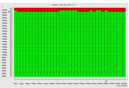
sub-system. . . 89 4.10 Area breakdown of the seven sub-systems. . . 91 4.11 Verigy test platform. . . 92 4.12 Frequency and skew sweep in the Asynch Hybrid Slow
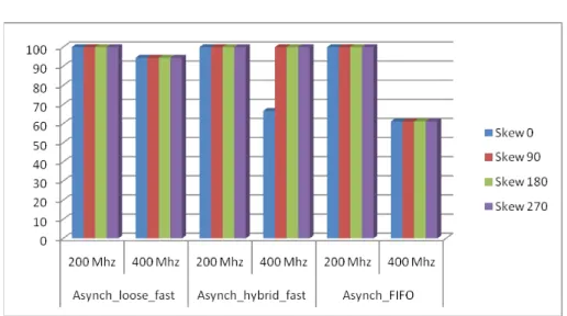
4.13 Frequency and skew sweep in the Asynch Loose Slow sub-system. . . 98 4.14 Percentage of working chips in each test case. . . 101 4.15 Relative power comparison. . . 102 5.1 Modular structure of the baseline switch architecture. Not all
connections are showed. . . 110 5.2 LBDR logic and requirements on the diagnosis outcome. . . . 111 5.3 The cooperative and concurrent testing framework saving TPG
instances and covering their faults. . . 114 5.4 Practical implementation of communication channel testing. . 116 5.5 TPG for communication channels. . . 117 5.6 BIST-enhanced switch architecture. . . 121 5.7 Area overhead for BIST implementation as a function of target
speed. . . 122 5.8 Coverage of TPG faults. . . 123 5.9 Latency breakdown of a scan chain-based test. . . 126 5.10 Practical implementation of the proposed scan chain-based test. 129 5.11 Maximum number of test patterns. . . 130 5.12 Latency of the scan chain-based test. . . 130 5.13 Total number of bits stored by the test patterns generator. . . . 131 5.14 Area overhead breakdown of the customized scan
chain-enabled testing strategy. . . 131 5.15 Area overhead breakdown of the scan chain-based and
deter-ministic test patterns-based solutions. . . 132 5.16 Latency of the scan chain-based and deterministic test
pattern-based solutions. . . 132 5.17 Coverage of the scan chain-based and deterministic test
pattern-based solutions. . . 133 5.18 Optimization steps of the pseudo-random testing framework. . 138 5.19 BIST-enhanced switch architecture. . . 140 5.20 Coverage for single stuck-at faults as a function of the test
la-tency. . . 141
5.21 Area overhead for BIST implementation. . . 141 5.22 Coverage for single stuck-at faults as a function of the test
la-tency. . . 143 5.23 Routing delay for BIST implementations. . . 144 5.24 Area overhead for BIST implementations. . . 145 5.25 Cooperative testing framework for bisynchronous
communi-cation channels. . . 148 5.26 Baseline bisynchronous communication channel. . . 149 5.27 Multisynchronous testing framework. . . 151 5.28 Proposed triple-stage brute-force synchronizer (a) and
wave-forms of synchronizers without (b) and with (c) set port. . . . 152 5.29 Bisynchronous channel operating principle. . . 155 5.30 Single stuck-at faults coverage as a function of test pattern
count (a) and area overhead for BIST implementation (b). . . . 158 5.31 Bisynchronous framework test time as function of ATA and
TPG frequencies. . . 159 6.1 Two NoC configurations where the routing algorithm needs to
be adapted. . . 164 6.2 Channel dependency graph for two routing algorithms and the
combination of both. . . 167 6.3 Reconfiguration steps performed in an OSR environment. . . 168 6.4 Token advance in a network: (a) check for absence of old
mes-sages and input ports epoch, (b) token signal propagation. The token separates old traffic from new traffic. . . 169 6.5 Reconfiguration steps performed in an OSR-Lite environment. 170 6.6 Switch input buffer enhanced with the OSR-Lite logic and a
new set of routing mechanism. . . 172 6.7 Switch arbiter enhanced with the OSR-Lite logic. . . 174 6.8 Switch output buffer enhanced with the OSR-Lite logic. . . 174 6.9 Configuration information from neighbor switches and control
6.10 OSR-Lite propagation over a 4 × 4 2D mesh topology: (a) scrolling up, and (b) scrolling down. . . 177 6.11 (a) Average message latency at different injection rates for SR
routing on 8 × 8 2D mesh (b) OSR-Lite propagation over a 8 × 8 2D mesh topology at different injection rates. . . 178 6.12 Average message latency with (a) hotspot traffic and uniform
traffic ((b) medium network load and (c) high network load). . 180 6.13 5x5 switch (a) area and (b) routing delay comparison. . . 182 7.1 Fault tolerant arbiter implementation. . . 195 7.2 Nack-Go switch . . . 197 7.3 OSR-Lite logic extended for the NACK/GO input buffer. . . . 199 7.4 Counter of packets of the two epochs. . . 200 7.5 Configuration information from neighbor switches and control
network . . . 201 7.6 OSR-Lite logic extended for the NACK/GO output buffer. . . 201 7.7 Fault-tolerant OSR-Lite logic. . . 203 7.8 Transient fault notification. . . 204 7.9 Dual network routing primitive. . . 205 7.10 TMR approach with per-primitive voting system. . . 206 7.11 Pratical implementation of data-path testing. . . 207 7.12 BIST-enhanced switch architecture. . . 210 7.13 Area of the GP-NaNoC switch. . . 212 7.14 Routing delay. . . 213 7.15 Efficiency of Single-LBDR implementation. . . 214 8.1 VC707 baseline prototyping board. . . 220 8.2 FPGA platform overview. . . 222 8.3 Design flow for platform implementation. . . 224 8.4 Basic components of the on-chip network. . . 225 8.5 LBDR routing logic extension for two cores per switch support. 228 8.6 The matrix multiplication at work. . . 230
8.7 The semaphores of the matrix multiplication application. . . . 232 8.8 Layout of the full FPGA design. Green: data NoC; red:
Net-work Interfaces; yellow: dual NoC; cyan: MicroBlazes and other logic. . . 234 8.9 Built-in-Self-Testing at work. . . 235 8.10 Transient fault detection and reconfiguration. . . 238 8.11 Network regions before (a) and after virtualization (b). Note
that the arrows indicate the logical application flow, not neces-sarily the route followed by packets. For case (b), the arrows are only indicative of partitioning, but the pipeline sequence is in fact shuffled for verification purposes. . . 241 8.12 Virtualization request and reconfiguration. . . 242
List of Acronyms and Symbols
ASIC Application-Specific Integrated Circuit CMP Chip MultiProcessor
CTS Clock Tree Synthesis
DVFS Dynamic Voltage and Frequency Scaling FF Flip-Flop
FHD Full High Definition FIFO First In First Out
FPGA Field Programmable Gate Array FSM Finite State Machine
GALS Globally Asynchronous Locally Synchronous GPP General Purpose Processor
GPU Graphics Processing Unit HDL Hardware Description Language IP Intellectual Property
ITRS International Technology Roadmap for Semiconductors LEF Library Exchange Format
LUT Look-Up Table
MIN Multi-stage Interconnection Network MPSoC Multi Processor System on Chip MUX Multiplexer
NI Network Interface NoC Network-on-Chip OCP Open Core Protocol P &R Place and Route PDA Personal Data Assistant RR Round Robin
RTL Register Transfer Level SOCE Cadence SoC Encounter SR Search&Repair
SoC System on Chip
TLM Transaction-Level Modeling TTM Time-to-Market
VLSI Very Large Scale Integration LBDR Logic-Based Distributed Routing TPG Test Pattern Generator
ATA Auto-Test Analyzer BIST Built-In Self-Test BISD Built-In Self-Diagnosis DUT Device Under Test TRC Two-Rail Checker
MISR Multiple Input Signature Register LFSR Linear Feedback Shift Register MTTF Mean Time To Failure
1
Introduction
T
HEembedded system market is rapidly growing and features a rich vari-ety of devices that are able to perform a wide multitude of diverse tasks. Nowadays, appliances such as mobile phones, personal data assistants (PDA) and ebook readers became mainstream in our everyday life. These mo-bile devices are ubiquitous, can be utilized everywhere and their applicability range span from pure computational tasks, through entertainment up to social network connectivity. The tremendous complexity reached by such devices represents a major challenge faced by engineers that have to design systems under a constant and relentless time-to-market (TTM) pressure. In order to shorten such TTM, the design of such devices is traditionally performed by integrating existing components in a plug–and–play fashion into a System-on-Chip (SoC) [1]. Therefore, a major challenge consists of interconnecting many different components with each other in an efficient way. According to ITRS roadmaps [103], thousands of cores will be integrated in a single chip during the next few years. Such scenario opens up many questions regarding scalabil-ity issues as all the cores in the single chip will have to be interconnected in a power efficient and scalable way.Classically, intellectual properties (IPs) (e.g., memory controller, CPUs, GPUs, etc.) designed by different vendors are interconnected by dedicated buses. AMBA, AXI, AHB [75, 76] represent well-established industrial exam-ples of such interconnection architectures. Unfortunately, they do suffer from well known scalability problems due to arbitration penalties. This is one of the driver dictating the adoption of a more scalable interconnection scheme: Networks-on-Chip (NoCs). NoC architectures represent a viable, scalable packet-switched micro-network interconnect scheme alternative to classical bus architectures [110]. They are generally believed to be the long term so-lution to the communication scalability issue.
CHAPTER1. INTRODUCTION
Today, networks-on-chips (NoCs) implement the communication backbone of virtually all large-scale system-on-chip (SoC) designs in 45nm and below. De-spite their fast diffusion in products and roadmaps, today’s NoC reality was not fully encompassed in the early position papers [2, 4]. After twelve years of trial-and-error, design experiences and focused research ( [3,5,7,8]), designers have gained the awareness of the profound difference of on-chip vs. off-chip interconnect design [13], of the tight constraints of an on-chip setting [6], of the challenges posed by nanoscale technologies [9] and of the differentiated re-quirements of specific application domains [10](e.g., application-specific het-erogeneous NoCs vs. general-purpose homogeneous NoCs). As a result, NoC design principles have recently reached a stage where they start to stabilize, in correspondence to their industrial uptake [11, 12].
Unfortunately, the requirements on embedded system design are far from sta-bilizing and an unmistakable trend toward enhanced reconfigurability is clearly underway. Reconfigurability of the HW/SW architecture would in fact enable several key advantages, including on-demand functionality, on-demand accel-eration, shorter time-to-market, extended product life cycles and low design and maintenance costs. Supporting different degrees of reconfigurability in the parallel hardware platform cannot be however achieved with the incremen-tal evolution of current design techniques, but requires a disruptive approach and a major increase in complexity. At the same time, fault tolerance was previously an issue only for specific applications such as space or avionics. Today, due to the increased variability of components and breadth of operating environments, reliability becomes relevant to mainstream applications. Sim-ilarly, new reliability challenges cannot be solved by using traditional fault tolerance techniques alone: the reliability approach must be part of the overall reconfiguration methodology.
An even more daunting challenge for NoC designers consists of coming up with synchronization strategies for systems where the chip-level synchroniza-tion assumpsynchroniza-tions have been relaxed. Tradisynchroniza-tional globally synchronous clock-ing circuits have become increasclock-ingly difficult to design with growclock-ing chip size, clock rates, relative wire delays and parameter variations. Additionally, high speed global clocks consume a significant portion of system power and lack the flexibility to independently control the clock frequencies of submod-ules to achieve high energy efficiency. Therefore, ad-hoc counter measures must be adopted to relax the synchronization assumption within the system. In the highly parallel landscape of modern embedded computing platforms, the system interconnect serves as the framework for platform integration and
is therefore key to materializing the needed flexibility and reliability properties of the system as a whole. Therefore, time has come for a major revision of cur-rent NoC architectures in the direction of relaxed synchronicity and increased reconfigurability and reliability.
In addition, a key property that novel NoCs cannot miss is to guarantee a po-tentially fast path to industry, since NoC deployment is today a reality. An important requirement for this purpose is the efficient testability of candidate NoC architectures. This property is very challenging due to the distributed na-ture of NoCs and to the difficult controllability and observability of its internal components. When we also consider the pin count limitations of current chips, we derive that NoCs will be most probably tested in the future via built-in self-testing (BIST) strategies.
Although there is still ample room to research novel approaches to the spe-cific challenges of the NoC architecture, one key concern for this new re-vision round will be to co-design the solutions to different challenges in an integrated framework. In practice, interdependencies between different NoC features should be detected ahead of time so to avoid the engineering of highly optimized solutions to specific problems that however coexist inefficiently to-gether in the final NoC architecture.
The major contribution of this thesis consists of taking on the challenge of engineering a NoC architectures for the next generation of multi-synchronous, highly reconfigurable and reliable systems. The thesis tackles the challenge in three ways:
• Provides design methods able to overcome the conventional way of im-plementing testability, reconfigurability and multi-synchronous designs. In fact, synchronization interfaces are proposed and optimized in terms of area, latency and power bringing a large energy savings that make a multi-synchronous NoC affordable at almost the same area and power cost of its synchronous counterpart. In the reliability context, the the-sis presents four testing methods based on built-in test and self-diagnosis infrastructures making efficient use of NoC structural redun-dancy in cooperative testing frameworks. Ultimately, the reconfiguration is performed by means of a cost-effective, complete and transparent re-configuration process that has never implemented on-chip before and is able to drain at run-time the network at link/router level.
• The thesis detects the interdependencies between the different design features and addresses them all in a coherently integrated final NoC
CHAPTER1. INTRODUCTION
switch. The design methods for testability, reconfigurability and multi-synchronous designs are co-designed, co-optimized and finally inte-grated with state-of-art fault-tolerant techniques to coexist efficiently in the final NoC architecture.
• The proposed design methods have been validated by means of ASIC implementation and FPGA prototyping proving the practical relevance of the thesis research. The synchronization interfaces have been in-tegrated in the first multi-synchronous ASIC demonstrator in 40 nm CMOS process. On the contrary, methods for testability and reconfig-urability require non silicon-dependent strategies and they have been validated on a leading-edge Virtex-7 FPGA.
In the next section, we will start by looking at the problem of the synchroniza-tion design (Secsynchroniza-tion 1.1.1). Then Secsynchroniza-tion 1.1.2 presents the challenges related to reliable systems while Section 1.1.3 illustrates the issues of NoC reconfig-urations. The key approach proposed in this thesis is described in Section 1.2 and finally, Section 1.3 provides an overview of the remaining chapters of the thesis.
1.1
Problem Formulation
While technology is providing unprecedented levels of system integration, it is also bringing new severe constraints to the forefront: power budget restric-tions, overheating concerns, circuit delay and power variability, permanent faults affecting the system right from the beginning (manufacturing faults) or with progressive onset (wear-out faults), increased probability of transient faults. Such constraints are driving the migration into new forms and shapes of synchronicity, reconfigurability, testability and fault-tolerance. Hereafter chal-lenges brought by the design of these latter features are detailed with emphasis on the inability of current NoC literature to effectively tackle them as a whole in a single integrated framework.
1.1.1 The synchronization design issue
The maximum operating speed of the network architecture should not con-strain the speed of the networked IP cores. This calls for proper decoupling at the network boundary by means of synchronization interfaces. This is a key requirement also for power management strategies in the embedded computing
1.1. PROBLEMFORMULATION
domain, requiring each core to run at an independent and runtime variable volt-age and speed. Nowadays, both application requirements and technology ef-fects call for a disruptive evolution of the synchronization architecture. In fact, distributing a global clock throughout the entire chip with tighly controlled skew is becoming increasingly power inefficient and even infeasible. Indeed, shifting the focus to a pure silicon technology viewpoint, there are some other very important challenges to be faced by both industry and academic research. In fact, as technology advances into aggressive nanometer-level scaling, sev-eral design challenges emerge from technology constraints which require a continuous evolution of the interconnection implementation strategy adopted at the circuit and architectural levels. Synchronization of current and future chips with a single clock source and negligible skew is extremely difficult if not close to be impossible [1]. Indeed, synchronization is today definitely among the most critical challenges in the design of a global on-chip communication infrastructure, as emerging technology variability, signal integrity, power dissi-pation limits are contributing a severe break-down of the global synchronicitiy assumption when logical structures spans more than a couple of mm on the die [14]. NoCs typically span the entire chip area and there is now little doubt on the fact that a high-performance and cost-effective NoC in 45nm and be-yond can only be designed under relaxed synchronization assumptions [86]. A solution would be to design such systems using a fully asynchronous global intra-chip communication. Such choice would eliminate the clock distribution concern and would make designs more modular since timing assumptions are explicitly handled in the hand-shaking protocols. Unfortunately, current design tools and IP libraries heavily rely on the synchronous paradigm instead, thus making intermediate solutions more attractive and affordable in the short run. As previously anticipated, synchronizer-based globally asynchronous locally synchronous (GALS) systems represent an appealing solution in the mid term, and is therefore the focus of this thesis. In such systems, the design can be par-titioned in different frequency islands and the interconnection infrastructure can be envisioned as mesochronous domain (isolated by dual-clock FIFOs at the boundary) where a single clock spans the whole communication infrastruc-ture area relying on a loose synchronization assumption. Such mesochronous assumption allows to tolerate an arbitrary amount of space dependent time-invariant phase offset (i.e., skew) among the leaves of the clock signal hence resulting in a lower power clock tree synthesis. Unfortunately, the high cost of traditional synchronizer implementations in terms of area, power and latency is typically the main reason preventing their adoption as intermediate solu-tion. Moreover, this is only one of the possible GALS implementation variants
CHAPTER1. INTRODUCTION
within a large design space where it is difficult to select the best solution for the underlying design. Last, there is a general skepticism of industrial design-ers to relax the synchronization assumption in their chips due to the usage of unconventional tool capabilities, to the poor predictability of resulting designs and to the threat of process variations.
Aware of these challenging problems, the first goal of this thesis is to develop all the required support for the building process of such GALS systems. In particular, our contribution and emphasis is on the NoC infrastructure that is augmented with all the necessary library components in a sort of galsification process. Such GALS blocks are designed to considerably reduce area, power and latency issues. Furthermore, we perform a crossbenchmarking between implementation variants, resulting in actual guidelines for designers that want to migrate from synchronous to GALS solutions. Finally, the development effort of the synchronization library is validated with the tape-out of the first multi-synchronous ASIC demonstrator in 40 nm CMOS process.
1.1.2 The Built-In Self-Testing
On-chip interconnection networks are rapidly becoming the reference commu-nication fabric for multi-core computing platforms both in high-performance processors and in many embedded systems [15, 24]. As the integration densi-ties and the uncertaindensi-ties in the manufacturing process keep increasing, com-plementing NoCs with efficient test mechanisms becomes a key requirement to cope with high defect rates [16, 43]. Above all, the NoC testing infrastructure should not be conceived in isolation, but should be coherently integrated into a reliability framework taking care of fault detection, diagnosis and network reconfiguration and recovery to preserve yield [23].
Moreover, wear-out mechanisms such as oxide breakdown, electro-migration and mechanical/thermal stress become more prominent in aggressively scaled technology nodes. These breakdown mechanisms occur over time, therefore the methodology and the infrastructure used for production testing should be designed for re-use during the system lifetime as well, thus enabling graceful degradation of the NoC over time.
The detection and identification of failures is the foundation of any reliability framework. Unfortunately, developing such a testing infrastructure for a NoC is a serious challenge. The controllability/observability of NoC links and sub-blocks is relatively reduced, due to the fact that they are deeply embedded and spread across the chip. Also, pin-count limitations restrict the use of I/O pins
1.1. PROBLEMFORMULATION
dedicated for the test of the different NoC components. Traditional approaches to NoC testing rely on full-scan or boundary scan testing, but cannot avoid the significant overhead associated with the design for testability (DfT) infrastruc-ture [45]. Moreover, the resulting test application times and test pattern gen-eration times are hardly affordable for applications of practical relevance. A number of other concerns were raised in [44] on the use of external testers for nanoscale chip testing:
• First, the lack of scalability of test data volumes with the number of gates hidden behind each package pin.
• Second, the need for testing at full clock speed, which is overly expen-sive if even possible to accomplish with external testers.
• Third, the poor suitability of these latter for lifetime testing (and not just for production testing) and for a test-and-repair testing approach (beyond the baseline go/no-go philosophy).
As an effect, a migration from external testers to built-in self-test (BIST) in-frastructures was envisioned in [44], and was later confirmed by the large amount of works in the open literature targeting scalable BIST architectures for NoC testing [26, 46, 47]. At the same time, the limited fault coverage that functional and pseudo-random testing can achieve on the control path of NoC switches when test generators are outside the switch has further pushed the adoption of BIST units at least for such control blocks [17].
While BIST techniques seem the best suitable solution to tackle permanent failures in NoCs, transient faults can not be handled by such strategies as they appear and disappear unpredictably. BIST techniques must be therefore inte-grated in fault-tolerant systems able to satisfy the high reliability constraints imposed by modern environments. In this direction, this thesis does not simply propose methods based on full BIST strategies but it also provides methods to integrate and optimize the BIST mechanisms in fault-tolerant systems. In particular, the thesis proposes four different BIST strategies and the coher-ent integration of the most promising of them in a fault-tolerant switch micro-architecture thus able to address both permanent and transient failures. A key principle of the thesis approach consists of exploiting the inherent structural redundancy provided by NoCs. Each switch is comprised of input ports, out-put ports, arbiters and FIFOs that are duplicated for each channel. This feature is used to develop a very effective test strategy which consists of testing mul-tiple identical blocks in parallel and of cutting down on the number of test
CHAPTER1. INTRODUCTION
pattern generators. This is done both at the abstraction level of the switch micro-architecture (e.g., testing of the output port arbiters in parallel) and of the NoC architecture (i.e., testing of all NoC switches in parallel). The inher-ent parallelism of our BIST procedure makes our testing infrastructure highly scalable and best suited for large network sizes.
The proposed BIST procedures are suitable both for production and for life-time testing, and is complemented by a built-in self-diagnosis logic distributed throughout the network architecture able to pinpoint the location of detected faults in each switch. This diagnosis outcome matches the reconfigurability requirements of logic-based distributed routing and is therefore the stepping stone into the novel network reconfiguration strategy that will be proposed in this thesis and described in next sections.
1.1.3 The Reconfiguration Framework
As technology advances chip multiprocessors (CMPs) and multiprocessor systems-on-chip (MPSoCs) have been accepted as the method to enhance the computing power and the functionality of current high-end systems. An ever increasing number of cores and devices can be added to the same chip en-hancing its functionality and power. Current products already include tens and hundreds of devices (e.g. Tilera with 100 cores [25]). These systems rely on the Networks-on-Chip (NoC) concept where a high-performance interconnect is built inside the chip, allowing efficient interconnection between all the de-vices.
As complexity keeps increasing, there emerge new requirements that affect how the interconnect is designed. As mentioned in the previous sections, the system must support a wide range of faults. These latter impact the system con-figuration rendering the network affected. Besides reliability concerns, there is also an interest in providing further functionality to the system. Virtualiz-ing the entire chip into sets of virtual regions and assignVirtualiz-ing them to different applications running concurrently is appealing in those systems. Similarly, powering down unused resources during most of the time is becoming com-pulsory to keep power consumption levels to reasonable bounds. In both cases, the NoC component is affected as it needs to be reconfigured to the changing environment.
To address the new functionalities, the NoC must be enriched with an efficient reconfiguration process which enables the smooth and transparent transition between system configurations.
1.2. APPROACH
When the topology of the network changes, either involuntarily due to fail-ing/faulty components or voluntarily due to removal of addition of nodes, the network routing algorithm must be reconfigured in order to (re)establish full network connectivity among the attached nodes. In transitioning between the old and the new routing functions during network reconfiguration, additional dependencies among network resources may be introduced, causing what is referred to as reconfiguration-induced deadlock.
Current techniques typically handle this situation through static reconfigura-tion, meaning that application traffic is stopped and, usually, dropped from the network during the reconfiguration process. While this approach guarantees the prevention of reconfiguration-induced-deadlock, it can lead to unaccept-able packet latencies and dropping frequencies for many applications, particu-larly realt-time and quality-of-service (QoS) applications.
As alternative it can be implemented a dynamic reconfiguration. This latter allows user traffic to continue uninterruptedly during the time that the net-work is reconfigured, thus reducing the number of packets that miss their real-time/QoS deadline. However such technique requires effort to avoid deadlock situations and typically brings extra resources to the network.
In this thesis we advance state-of-the-art in reconfiguration frameworks for NoC-based systems. Anyway, instead of designing a brand new reconfigura-tion mechanism, it is recognized the large amount of bibliography and propos-als made for reconfiguration mechanisms in high-performance off-chip net-works. In this sense, it is picked the approach that better suits the NoC domain and the tight resource budgets of the on-chip environment. However, in its na-tive form its implementation in NoCs is out-of-reach. Therefore, we provide a careful engineering of the NoC switch architecture and of the system-level infrastructure to support a cost-effective, complete and transparent reconfigu-ration process.
1.2
Approach
This thesis takes on the challenge of designing the next-generation of multi-synchronous, reliable, and reconfigurable embedded systems by proposing new effective ad-hoc methods and by capturing their interdependencies in a co-designed and co-optimized final architecture.
Specifically, in order to tackle the synchronization problem, we design novel globally asynchronous locally synchronous (GALS) interfaces able to meet
CHAPTER1. INTRODUCTION
different layout constraints. In particular, we design dual-clock FIFO inter-faces to provide frequency decoupling between domains and mesochronous interfaces to relax the constraints of the clock tree within a frequency domain. The proposed interfaces are able to show that it is possible to migrate from the synchronous to the GALS paradigm with a negligible area and power cost without impacting performance.
The thesis also proposes and validates methods for reliable and reconfigurable embedded systems. Firstly, we present four scalable built-in test and self-diagnosis infrastructures making efficient use of NoC structural redundancy for testing and diagnosis purposes through the use of a cooperative testing frame-work. Secondarily the best suited proposed BIST framework has been inte-grated in an advanced multi-features switch, called GP-NaNoC. This latter in-tegrates the most relevant and innovative design methods conceived throughout the thesis and makes sure they co-exist together. The switch is enhanced with a transparent system reconfiguration mechanism, called Overlapping Static Re-configuration (OSR-Lite), and a novel flow-control protocol based on detec-tion, correction and retransmission providing fault-tolerance to the switch.
1.2.1 Validation Strategy
All the proposed design methods have been validated by means of demonstra-tors able to prove their practical relevance. In particular, two ad-hoc demon-strators have been implemented in order to ensure the robustness and the ef-fectiveness of the proposed design methods. The synchronization methods have been validated through an ASIC demonstrator in 40 nm CMOS process while the testability and reconfigurability methods have been implemented on a Virtex-7 FPGA prototype. Both technology and switch fabric adopted for the demonstrators have been consciously chosen to properly validate the underlin-ing design methods that they integrate.
The synchronization interfaces have been integrated in the first multi-synchronous ASIC demonstrator in 40 nm CMOS process. The tape-out on silicon served as demonstrator of the robustness of the synchronization inter-faces against process variability and operating conditions (e.g., speed ratio, clock phase offset). The demonstrator for synchronization methods improves the maturity of the developed GALS technology and bridges the final gap to actual silicon implementation. In particular, the testchip design and fabrication process validates the feasibility and effectiveness of the developed GALS NoC concept in nano-scaled technology sub-systems by comparing synchronous and GALS synchronization technology in a homogeneous experimental
1.3. ORGANIZATION
ting: same baseline designs, same manufacturing process, same die. Finally, the testchip fabrication breaks the barriers that have prevented the success of synchronizer-based technology for GALS NoCs so far in alternative design experiences.
As mentioned, ASIC technology is adopted to prove the robustness of synchro-nization interfaces against timing constraints of integrated circuits. Indeed the strict dependency of these latter methods to constraints proper of ASIC tech-nology did not allow us to consider alternative technologies for the first demon-strator. On the contrary, FPGA technology has been chosen to implement the second demonstrator integrating non-silicon dependent methods. In fact, testability and reconfigurability methods have been validated together with fault-tolerant techniques and control signaling strategies in a Xilinx Virtex-7 FPGA. In particular, a switching fabric based on the GP-NaNoC switch sup-porting network partitioning and isolation as well as irregularities has been designed and prototype on the second FPGA-based demonstrator. This lat-ter especially validates boot-time testing and configuration, runtime detection of faults, runtime reconfiguration of the routing function, dynamic virtualiza-tion of the switching fabric. The NoC prototype implemented on the second demonstrator is a key enabler for the materialization of the needed flexibility and reliability properties of next-generation embedded systems.
1.3
Organization
The contributions of this thesis are organized in 9 chapters. Before present-ing the contributions, Chapter 2 first provides the necessary background of the work in this thesis. It surveys built-in-self-testing, fault-tolerant and re-configuration strategies as well as globally-asynchronous locally synchronous interfaces for the building of GALS systems. Finally, it summarizes the short-coming of the presented work to be addressed in subsequent chapters.
Chapter 3 introduces the synchronization design issue. In a first step, the moti-vation for adopting synchronization mechanisms in the NoC environment will be discussed. Next, the target GALS platform of this thesis along with the architecture of the basic switch block required to build it will be highlighted. Last, it is presented the baseline mesochronous synchronizer and the dual-clock bi-synchronous FIFO with focus on all their improvements that led to a new fully integrated and flexible switch architecture.
Chapter 4 presents the GALS ASIC demonstrator in 40 nm CMOS process. The chip, named Moonrake, validates on silicon the robustness of the GALS
CHAPTER1. INTRODUCTION
interfaces proposed in the previous Chapter. Firstly it is described the testing environment setup and the floorplanning constraints of the chip. Later, the dif-ferent GALS subsystems integrated into the chip are presented with their own synchronization properties. Finally, the experimental section presents the per-formance of the subsystems.
Chapter 5 provides an exploration of built-in testing strategies customized for NoC-based systems comparing them under an area, coverage and latency point of view. In particular, the first section proposes a BIST mechanism exploiting architecture behavior knowledge to come up with a set of customized test pat-terns for NoC components. The second section presents a strategy based on a scan chain mechanism. In the third section, we design a testing based on pseudo-random patterns where we cut down on the test application time and we provide efficient testing of the control path. In the fourth section, we pro-pose one of the first built-in self-testing and diagnosis framework for globally-asynchronous locally-synchronous NoC based on an globally-asynchronous handshak-ing.
Chapter 6 presents the implementation of the fast and transparent reconfigu-ration mechanism called OSR-Lite. The Chapter describes the complete re-configuration mechanism at work, involving the BIST mechanism, a central manager and a notification infrastructure. It is showed the implementation at micro-architecture level of the logic enabling the mechanism and the propaga-tion of the reconfigurapropaga-tion tokens. Finally, the OSR-Lite mechanism is evalu-ated in terms of area and latency.
Chapter 7 extends the work presented in the previous chapters by propos-ing a switch (GP-NaNoC switch) integratpropos-ing BIST, reconfiguration and fault-tolerance features in a single co-designed architecture. First of all, the switch architecture extensions for fault tolerant NoC design are presented. Especially, it is highlighted a novel protocol (NACK/GO) based on retransmission and a fault-tolerant arbiter. Thus the Chapter presents the optimizations introduced in the BIST mechanism and the OSR-Lite logic achieved by co-designing the reconfiguration and testing strategies with the fault-tolerant architecture. Next, the switch extensions for system level notification are described and coverage, area and critical path of the novel switch are finally reported.
Chapter 8 reports about the prototyping of the design methods proposed in the previous Chapters on a Xilinx Virtex-7 FPGA. The FPGA prototype com-prises a large number of components that enables observability, controllability and debugability of the system under test. All this components are described in detail. Last, it is illustrated the application running on the system and the strategies adopted to validate the BIST, the fault-tolerance and the
1.3. ORGANIZATION
ration features of the system.
Finally, Chapter 9 provides concluding remarks on the work presented. The chapter summarizes the thesis and outlines its contributions.
2
Background
T
HISchapter starts by surveying several works in the domain of globally asynchronous locally synchronous (GALS) Networks-on-Chip. Fur-thermore, contributions concerning testing techniques and fault-tolerant systems are also surveyed. Last, works in the domain of network reconfigu-ration are reported. The chapter highlights also the contribution of this thesis with respect to the work available in the open literature.2.1
The GALS Design Style
When the target system requires the interconnection of several components working at different frequency, the adopted synchronization scheme and its implementation is key for a successful result of the final system design. A possible solution is to adopt the GALS philosophy which can be seen as an intermediate design style between the fully synchronous and fully asyn-chronous solutions. The GALS design paradigm was first proposed in [131] and consists basically of partitioning the system architecture in independent synchronous islands while the communication between them is achieved asyn-chronously. It is therefore a natural enabler for low-power dynamic volt-age and frequency scaling (DVFS) and low noise. The GALS paradigm has been frequently experimented by using asynchronous logic [87, 89]. ETH labs developed a complete GALS methodology leveraging the use of paus-able clocks [68]. IHP labs designed a 802.11a GALS baseband processor in-cluding various IP cores, a viterbi decoder, FFT, IFFT and a Cordic processor. Several asynchronous NoCs have been also proposed: Mango [89], QNoC, ANoC, CHAIN [130], FAUST [95], Alpin, Magali. A chip dedicated to flex-ible baseband processing for 3G/4G wireless telecommunication applications and making use of an asynchronous NoC is described in [83, 84]. However,
CHAPTER2. BACKGROUND
currently the intricacy of asynchronous design and its poor CAD tool support makes the design of hard macros with ad hoc techniques [77] the only viable solution for industrial exploitation [85]. This comes at the cost of large area and penalizes flexibility.
The practical viability of synchronizer-based GALS networks has been demon-strated in [95], where the hierarchical clock tree synthesis technique for such systems is detailed. A circuit switched source synchronous GALS link is de-scribed in [82], making use of long distance interconnect paths. It is then experimented on a 65nm reconfigurable NoC for an heterogeneous GALS many-core platform. However, there is no comparison whatsoever with alter-native clocking styles and/or implementations. In [129] a many-core hetero-geneous computational platform employing GALS compatible circuit switch-ing on-chip network has been presented. [115] presents an example of mesh-connected GALS chip multiprocessor. The work shows that the typical perfor-mance penalties of GALS systems (mainly due to additional communication latency) can be hidden by using large FIFO buffers. In [95], the physical im-plementation of the DSPIN network-on-chip in the FAUST architecture has been presented. In [116] a cost effective solution for asynchronous delay-insensitive on-chip communication is proposed. The solution is based on the Berger coding scheme and allows to obtain a very low wire overhead. [119] proposes a new asynchronous NoC architecture aiming at low latency trans-fers. This architecture is implemented as a GALS system, where chip units are built as synchronous islands, connected together using a delay insensitive asynchronous Network-on-Chip topology.
2.1.1 The dual-clok FIFO Synchronization Interfaces
From the pure fully asynchronous world, there are several examples of FIFOs in literature [120, 121]. Since these designs do not utilize clocks, they are difficult to be adopted when two different clock domains have to be synchro-nized (e.g., two frequency islands of a GALS system). A reliable data transfer across unrelated asynchronous clock domains is accomplished by [122]. This work is demonstrated in both standard cell and full custom design used in a GALS array processor. In any case, the presented synchronizer does not ac-count for timing implication when integrated in the NoC domain. The work in [123] illustrates a modular and easily configurable dual-clock FIFO for dif-ferent NoC requirements (clocked or clock-less interfaces, synchronization la-tency for resolving metastability, FIFO capacity). This design was inspired by the modular FIFO from [124], composed of a ring of stages, where each
2.1. THEGALS DESIGNSTYLE
stage is composed of a storage cell, a put interface and a get interface. The solutions in [123] and [124] differ as [123] uses cells that are available from a typical standard cell library, whereas [124] requires custom, pre-charged cells in the control blocks. Nevertheless, [123] achieves performance which is com-parable or even slightly higher than that reported in [124] when scaling for the different fabrication technologies. Furthermore, [123] separates the FIFO control logic from the synchronizers, allowing the synchronization latency to be chosen according to the clock frequency and reliability requirements. [136] proposed a synchronizing FIFO design based on read and write pointer com-parison using Gray codes. The result of the comcom-parison is synchronized to the sender’s and receiver’s clocks. Their design uses two binary counters for read and write addresses and a dual-port RAM for data storage which results in a larger and more complicated design for the modest FIFO capacities that are typically needed for NoC design. Furthermore, the design in [136] only provides FIFO capacities that are powers of two. The design in [137] uses the position of the read and write pointers to determine fullness and empti-ness condition. It employees one synchronizer to detect fullempti-ness, and a syn-chronizer per-stage to detect emptiness. To prevent errors due to metastability when sampling the pointers, they use two tokens each as the read pointer and write pointer. This makes their empty detector a little bit more complicated, as it requires comparing two synchronized write pointer bits with two read pointer bits for each stage. In addition, to differentiate between a full and an empty FIFO, they only fill the FIFO up to the second-to-last position, which means that a n stage FIFO can only hold n − 1 items.
The operating principle of the dual-clock FIFO architecture proposed in this thesis resembles that of [123]. From an implementation viewpoint, we were inspired by [137] and [136]. From [137], we borrowed the token ring concept for implementing FSMs, since this is a simple yet robust solution with respect to Grey coding. From [136] we borrowed the idea of performing a comparison between read and write pointers asynchronously and then synchronizing the result in the target domains. With respect to previous work, this thesis presents not just a single dual-clock FIFO architecture for use in the general case, but specializes the architecture for the specific operating conditions.
In general, a tight integration of synchronization interfaces into NoC building blocks to cut down on latency, area and power is advocated. Finally this thesis addresses the co-design of synchronizers with NoC building blocks.
CHAPTER2. BACKGROUND
2.1.2 The Mesochronous Synchronization Interfaces
For the particular case where the clocks in two communicating domains have the same frequency but unknown phase offset, then a dual-clock FIFO would be too much of an overhead and custom tailored mesochronous synchronizers are normally more cost-effective. Several works leverage the timing determin-ism provided by GALS wrapper to facilitate debug and testing of GALS sys-tems [133], [134]. A mesochronous link is integrated within a multi-processor tiled architecture based on a Network-on-Chip communication backbone on a CMOS 65nm technology in [80]. The work builds on a full-duplex link ar-chitecture illustrated in [79] and on integrated flow control [78]. The baseline mesochronous synchronizer is instead proposed in [96]. However, the synchro-nizer is still an external module to the NoC. The same drawback is exposed by a different synchronization architecture, detailed in [97].
Examples at industrial level are presented in [99], [98], [114], [96]. In [98] au-thors examine the use of GALS techniques to address on-chip communication between different synchronous modules on a bus. Issues related to valida-tion, module interfaces and tool flows, while looking at advantages in power savings, timing closure and Time-to-Market/Time-to-Money (TTM) are ex-plored. [114], [96] both suggest to implement the boundary interface with a source-synchronous design style and propose some form of ping-pong buffer-ing to counter timbuffer-ing and metastability concerns.
A well established solution for mesochronous synchronization is illustrated in [128] consists of delay-line synchronizers, using a variable delay on the data lines. This delay is computed in such a way to avoid switching in the metastability window of the receiving registers. Variable delay lines make this solution expensive and not always available in standard cell libraries. This is the same problem of the works in [117, 118], which use voltage comparators. Several periodic synchronizers are illustrated in [112], which avoid metastabil-ity by delaying either the data or the clock signal to sample data when the clock is stable. Configurable digital delay lines are again needed and experimented frequency is very low. The same authors in [132] illustrate many ways to “fool” a synchronizer thus showing several weaknesses of the proposed approaches. The works in [94,100,117] achieve mesochronous data synchronization by us-ing Muller C-elements and digital delay lines that are typically designed with a full-custom approach. [100] presents a self-tested self-synchronization method for mesochronous communication. The scheme uses two clocks with a phase shift of 180◦and a failure detector is used to select which one to use. In [94] a phase detector in place of a metastability detector is used in the same scheme.
2.2. RELIABILITY
Architectures based on FIFO synchronizers are proposed in [101, 123, 128]. FIFO size in [101] depends on the skew, hence is link-dependent or given in the worst-case. Implementation is also very expensive, as showed in [102]. More recently, an optimized bi-synchronous FIFO has been proposed in [137] fea-turing low-latency and small footprint. It can be adapted to the mesochronous needs while proving able to tolerate skew only up to 50% of the clock period. An early mesochronous scheme for the SoCBus NoC was proposed in [81], aiming at compact realization while still lacking of a validation on an NoC test case. A significant step forward comes from the OCN system [113], which uses a source synchronous scheme. A matched-delay architecture is used to compensate the strobe skew and enable high-speed mesochronous communi-cation. A FIFO synchronizer is used at the receiver side.
Summing up, mesochronous synchronizers surveyed so far incur several dis-advantages: high implementation overhead, use of non-trivial or full-custom components or low skew tolerance. Moreover, very few works are able to as-sess timing margins with layout awareness. In this thesis, the same approach to synchronization of [96, 109] is taken (source synchronous data transmis-sion, safe storage of data at the receiver side, sampling in the receiver domain only when data is stable). However, the baseline architectures and circuits are improved by providing a more compact and equally robust solution. This is used just as the baseline architecture for the sake of comparison with the novel synchronization structure that it is proposed.
The tight synchronizer-NoC coupling design principle adopted for the dual-clock FIFOs is followed also for the mesochronous synchronizer to cut down on area, latency and power. Furthermore, a wide range of architecture alter-natives and even port-level configuration capability is provided. Moreover, we identify the distinctive design constraints of the new schemes and perform a design space exploration of mesochronous NoC links and switches to capture how timing margins can be preserved for different combinations of synthesis and layout constraints.
2.2
Reliability
As faults will appear with increasing probability due to the susceptibil-ity of shrinking feature sizes to process variabilsusceptibil-ity, age-related degradation, crosstalk, and single-event upsets, designing efficient reliable NoCs becomes a key requirement. However, errors can differently affect the system: they can produce permanent, intermittent or transient failures depending on their