UNIVERSITÀ DEGLI STUDI DI CATANIA
SCUOLA DI DOTTORATO
Dottorato di Ricerca Internazionale in Ingegneria dei
Sistemi – XXVIII
◦ciclo
Ph. D. Thesis
Fully integrated systems with
on-chip galvanic isolation in silicon
technology
Dott. Ing. Vincenzo Fiore
Tutor: Coordinator:
Prof. Giuseppe Palmisano Prof. Luigi Fortuna
External tutor: Dr. Egidio Ragonese STMicroelectronics, Catania
Summary
This thesis summarizes main activities that I have been carrying out at the Radio-Frequency Advanced Design Center (RFADC), a joint research center between STMi-croelectronics and the University of Catania, during my three years of Ph. D. studies. My principal activity was part of an RFADC research project which exploits an STMicroelectronics technology providing on-chip galvanic isolation. This available platform was previously addressed to the implementation of galvanic-isolated data transfer and it is currently used for mass production. In this context, the principal purpose of my work was the investigation on fully integrated systems providing on-chip galvanic isolation in a silicon technology. This research is mainly motivated by the higher level of integration that is demanded to the next generation of power con-verters and several other applications requiring galvanic isolation. In this field both data and/or power transfer are commonly required for sensing and control purposes, with typical applications requiring few tens of Mbps and less than 1 W for data and power transfer, respectively. Within this context, fully integrated interfaces can pro-vide several advantages, including higher reliability, lower PCB area, lower system complexity and hence lower costs, especially if only silicon technology is exploited. However, the state of the art of silicon-based integrated solutions mainly concern data-transfer devices, whereas for power transfer even the most advanced solutions rely on post-processed passive devices. These topics are presented in Chap. 1.
strategies to properly exploit the integrated approach. Therefore, this thesis focuses on fully-integrated systems, with the aim of filling this last gap by implementing also power transfer with silicon technology. This is a complex task that requires accurate evaluation of on-chip and off-chip parasitics, modeling of integrated passive devices, and customized active and passive circuit co-design. Specifically, my two principal activities are discussed in this thesis, that were the integration of a galvanically isolated, watt-level, step-up, power transfer system for gate driver’s power supply applications, and the design of two ASK data receivers for an innovative data/power transfer system. They are the object of Chap. 2 and Chap. 3, respectively, whereas my contributions to two more CMOS-based power transfer systems can be found in App. B. These systems have been integrated in the aforementioned technology and successfully characterized, showing comparable power and data transfer performance with respect to the state of the art. To the best of the author’s knowledge, these are also the first reported systems of this kind which do not require post-processing steps, therefore demonstrating the feasibility of power with/without data transfer on silicon technologies and thus promising new and highly-integrated devices to become available.
Besides these main topics, It is worth mentioning a secondary topic, carried out during the first year of my Ph. D. studies. Specifically, I actively contributed to the “COSMIC” Project, a second research project to which the RF-ADC participated in last years, in collaboration with the Technical University of Eindhoven, CEA-Liten, Fraunhofer Institute EMTF, and several other international partners. The COSMIC project was an FP7 research project in the field of organic and printed electronics. Organic electronics is seen as one of the most promising technology, especially if printed manufacturing techniques are used. By providing very low-cost electronics and flexible or wearable devices, its aim is to participate to the ubiquitous computing trend promised and renowned as the “Internet of Things”, and extend its
applications. For example, the availability of a printed radio-frequency identification (RFID) tag is a key target for printed electronics, which could further shrink the costs of RFID technology, thus enabling a wider range of applications to take advan-tage of it. However, current organic technologies offer very low performance, thus requiring proper design techniques and architectures to be introduced. As a main outcome of my contribution to this project, the implementation of an integrated 13.56-MHz RFID tag in a printed complementary organic thin-film transistors tech-nology (C-OTFT) on flexible substrate has been successfully demonstrated for the first time. This circuit is the most complex mixed-signal integrated system ever published in a printed C-OTFT technology, with more than 250 organic TFTs on the same foil. Its design and characterization are the object of two publications, [1] and [2].
Summary iii
List of Tables ix
List of Figures x
1 Introduction 1
1.1 Low-power isolated interfaces . . . 1
1.1.1 Applications . . . 2
1.1.2 State-of-the-art . . . 9
1.1.3 Isolator’s market . . . 20
1.2 Aim of this thesis . . . 23
1.2.1 Basic architecture . . . 24
1.2.2 Technology platform . . . 26
1.2.3 Main results . . . 28
2 A watt-level, step-up, power transfer system 31 2.1 System description . . . 31
2.2 Efficiency analysis and design issues . . . 36
2.2.1 Rectifier . . . 37
2.2.2 Isolation transformer . . . 39
2.2.4 Design issues . . . 52
2.3 System design . . . 54
2.3.1 Modeling of the stacked isolation transformer . . . 55
2.3.2 Co-design procedure and expected results . . . 60
2.3.3 Micrographs . . . 65
2.4 Measurement results . . . 68
2.4.1 DC-DC converter . . . 71
2.4.2 Isolation transformer . . . 75
2.4.3 DC-AC converter . . . 77
2.5 Comparison with the state-of-the-art . . . 83
3 A 40 Mbps/23 mW data/power transfer system 85 3.1 System description . . . 86
3.2 High sensitivity and low power ASK detectors . . . 90
3.2.1 Common-Source ASK detector with adaptive biasing . . . 93
3.2.2 High-Speed detector . . . 96
3.2.3 Low-Speed detector . . . 104
3.3 Measurement results . . . 109
3.3.1 Measurement setup . . . 109
3.3.2 High-Speed data transfer . . . 112
3.3.3 Low-Speed data transfer . . . 116
4 Conclusion 121 A Simplified expressions for RC -loaded transformers 1 B Circuit topologies and passive device modeling for CMOS-based systems 9 B.1 CMOS Topologies for power transfer systems . . . 9
List of Tables
1.1 Thresholds and limits for continuous 60 Hz current and their effects [3]. 8
1.2 System-level standards involving isolation by market and region [4]. . 8
2.1 Simulated rectifier performance, VOU T = 20 V, POU T = 1 W . . . 39
2.2 Summary of optimized designs from Fig. 2.17 . . . 64
2.3 Design parameters for the proposed converter. . . 65
2.4 Expected performance. . . 66
2.5 Comparison with state-of-the-art integrated step-up converters. . . . 83
3.1 Summarized design parameters and simulated performance of the HS detector. . . 103
3.2 Summarized design parameters and simulated performance of the LS detector. . . 108
B.1 Comparison between dc-dc converters fabricated in the same BCD technology adopted in this work. . . 14
1.1 Typical architectures for a motor drive [6]. . . 3
1.2 Ground loops problem in wireline communication systems [7]. . . 6
1.3 (a) Typical optocoupler structure. (b) X-ray cross section of a device. 10 1.4 Optocoupler equivalent circuit [8]. . . 11
1.5 (a) Typical capacitive isolator system [9]. (b) Photo of the system before packaging [10]. . . 12
1.6 Capacitive voltage partition at the rectifier’s input port. . . 14
1.7 Integrated inductive isolator architecture [11]. . . 15
1.8 (a) Planar isolation transformer. (b) Photo of an inductive isolated system before packaging [12]. . . 16
1.9 (a) Cross-section of isoPower transformer. (b) Photo of an inductive power/data transfer SiP [13]. . . 17
1.10 Simplified IEC 60747-5 and VDE 0884-10 test profiles [14]. . . 19
1.11 Simplified VDE 0884-10 surge test profile [14]. . . 20
1.12 Definition of clearance and creepage [15]. . . 20
1.13 Forecasts for worldwide isolation market [16]. . . 21
1.14 Typical low-power applications requiring isolated power transfer. . . . 23
1.15 Basic architecture for isolated power transfer. . . 25
1.16 Simplified cross-section of the available back end of line with thick oxide module for galvanic isolation. . . 27
2.1 Simplified schematic of the watt-level step-up dc-dc converter. . . 32
2.2 Simplified layout of the isolation transformer: (a) BEOL cross-section, (b) 3-D view of the transformer, (c) planar view of the primary coils, and (d) planar view of the secondary coils. . . 35
2.3 Power transfer flow diagram. . . 36
2.4 Rectifier efficiency as a function of the output power for different diode multiplicity, M. . . 38
2.5 Linear lumped transformer model. . . 41
2.6 Typical power transfer efficiency, ηT X_AC, for an integrated trans-former. . . 43
2.7 Simplified equivalent circuit of the dc-ac converter. . . 46
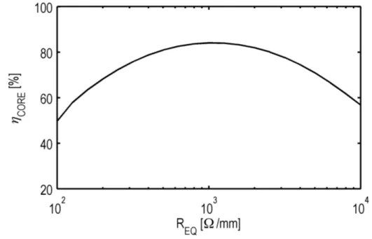
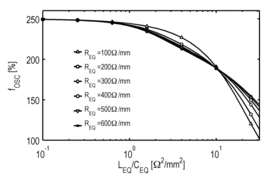
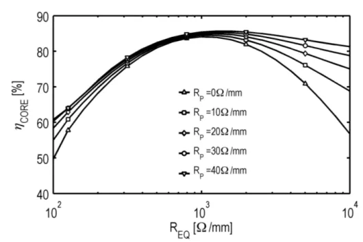
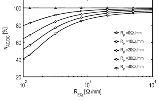
2.8 Oscillator performance as a function of LEQ/CEQ for RP = 0 Ω/mm. . 48
2.9 Oscillator performance as a function of REQfor LEQ/CEQ= 20 Ω2/mm2. 49 2.10 Oscillation frequency fOSC as a function of LEQ/CEQ for several REQ. 50 2.11 Oscillator performance as a function of REQfor LEQ/CEQ= 20 Ω2/mm2. 51 2.12 Oscillator PT X_AC/PT Xas a function of REQfor LEQ/CEQ = 20 Ω2/mm2. 52 2.13 Schematic of the lumped geometrically scalable model of the isolation transformer TISO (half-structure). . . 56
2.14 Error distributions of the geometrically scalable lumped model calcu-lated with respect to EM simulations. . . 59
2.15 Graphic representation of the proposed co-design procedure. . . 61
2.16 Equivalent tank impedance at the increasing of WA. . . 62
2.17 Typical results of the co-design procedure in Fig. 2.15 : (a) output ac power, POU T_AC, (b) dc-ac efficiency, ηDC−AC, (c) oscillator fre-quency, fOSC. . . 63
2.18 Micrograph of the power oscillator die. . . 67
2.19 Micrograph of the power rectifier. . . 67
TISO (half-structure). . . 69
2.22 Micrograph of the dc-ac converter assembled on board. . . 70 2.23 Output power, POU T, and power efficiency, η, as a function of the
output voltage VOU T. . . 71
2.24 Output power, POU T, and power efficiency, η, as a function of the
measurement time. . . 72 2.25 Power efficiency, η, versus output power, POU T, (VOU T = 20 V). . . 73
2.26 Power efficiency, η, versus output power, POU T, for different biasing
voltages VB (VOU T = 20 V). . . 74
2.27 Power efficiency, η, versus output power, POU T, for different supply
voltages VDD (VOU T = 20 V). . . 74
2.28 Narrowband parameters of the isolation transformer - measurements vs. simulation. . . 75 2.29 Wideband parameters of the isolation transformer - measurements vs.
simulation. . . 76 2.30 Output power measured at the transformer secondary winding as a
function of load resistance RL without external CL. . . 78
2.31 Power efficiency measured at the transformer secondary winding as a function of load resistance RL without external CL. . . 78
2.32 Oscillation frequency measured at the transformer secondary winding as a function of load resistance RL without external CL. . . 79
2.33 Output voltage measured at the transformer secondary winding for three values of load resistance RL without CL added. . . 79
2.34 Output power measured at the transformer secondary winding as a function of load capacitance CL for different RL. . . 81
2.35 Power efficiency measured at the transformer secondary winding as a function of load capacitance CL for different RL. . . 81
2.36 Oscillation frequency measured at the transformer secondary winding as a function of load capacitance CL for different RL. . . 82
2.37 Output voltage measured at the transformer secondary winding for three values of load capacitance CL (RL= 220 Ω). . . 82
3.1 Proposed architecture for isolated data/power transfer. . . 87 3.2 Simplified schematic of the isolated data/power transfer system [17]
©2016 IEEE. . . 87 3.3 (a) PWM coding scheme adopted. (b) Degradation of the detector’s
noise margin after long sequences of ones or zeros. . . 89 3.4 Traditional architecture of an ASK detector. . . 90 3.5 (a) Passive, and (b) Common-Drain envelope detectors. . . 91 3.6 Typical (ideal) waveform of the modulated signal at the NMOS
os-cillator drains, VD1/2 (see Fig. 3.2): (a) time domain, (b) frequency
domain. . . 92 3.7 (a) Traditional common source envelope detector. (b)
Common-source based ASK detector with adaptive biasing [18]. . . 95 3.8 Simplified schematic of the HS detector. . . 96 3.9 Loop gain THS(jω), and closed-loop trans-impedance ZL,HS, of the
HS detector. . . 98 3.10 Schematic of the HS error amplifier. . . 100 3.11 Simulated current consumption and conversion gain of the HS
detec-tor for a 5% modulated input signal, as a function of the peak input voltage, AP K, for the waveform in Fig. 3.6(a). . . 101
3.12 Simulated bias voltage of the HS detector for a 5% modulated input signal, as a function of the peak input voltage, AP K. . . 102
3.13 Schematic of the HS detector comparator. . . 102 3.14 Simplified schematic of the LS detector [17] ©2016 IEEE. . . 104
detector. . . 105
3.16 Simulated current consumption and conversion gain of the LS detector for a 5% and a 25% modulated input signals, as a function of the peak input voltage, AP K, for the waveform in Fig. 3.6(a). . . 107
3.17 Simulated bias voltage of the LS detector for a 5% and a 25% mod-ulated input signals, as a function of the peak input voltage, AP K. . . 107
3.18 Schematic of the LS detector comparator. . . 108
3.19 Micrograph of the CMOS isolated power/data transfer system [17] ©2016 IEEE. . . 110
3.20 Simplified description of the BER measurement setup. . . 111
3.21 Simplified flow-chart diagram of the BER measurement system. . . . 112
3.22 Measured HS data link waveforms at 2.5 Mbps. . . 113
3.23 Measured HS data link waveforms at 20 Mbps. . . 114
3.24 Measured HS data link waveforms at 40 Mbps. . . 115
3.25 Measured LS data link at 150 kbps. . . 117
3.26 Measured LS data link at 1 Mbps. . . 118
3.27 Measured LS data link at 3 Mbps. . . 119
A.1 Linear lumped transformer model: (a) Traditional topology, (b) equiv-alent representation without coupled inductors, (c) and (d) simplified models. . . 2
A.2 Modeling of the load impedance. . . 3
A.3 Comparison between simulated transfer efficiency for the circuit in Fig. A.1(a) and calculated values from Eq. A.11 vs. LP. . . 4
A.4 Comparison between simulated transfer efficiency for the circuit in Fig. A.1(a) and calculated values from Eq. A.11 vs. RP. . . 5
A.5 Comparison between simulated transfer efficiency for the circuit in Fig. A.1(a) and calculated values from Eq. A.11 vs. LS. . . 5
A.6 Comparison between simulated transfer efficiency for the circuit in Fig. A.1(a) and calculated values from Eq. A.11 vs. RS. . . 6
A.7 Comparison between simulated transfer efficiency for the circuit in Fig. A.1(a) and calculated values from Eq. A.11 vs. CRECT. . . 6
A.8 Comparison between simulated transfer efficiency for the circuit in Fig. A.1(a) and calculated values from Eq. A.11 vs. RRECT. . . 7
B.1 Transformer-loaded CMOS oscillators with equivalent rectifier impedance load, ZRECT: (a) Complementary cross-coupled oscillator, (b)
Current-reuse transformer-coupled oscillator [5] ©2015 IEEE. . . 12 B.2 Transformer-loaded CMOS oscillators with equivalent rectifier impedance
load, ZRECT: (a) Current-reuse transformer-coupled oscillator [5], (b)
Current-reuse hybrid-coupled oscillator topologies [19] ©2015 IEEE. 13 B.3 Isolation transformer schematic ©2015 IEEE. . . 15 B.4 Isolation transformer: (a) Primary windings, (b) Secondary winding,
and (c) 3-D view [5] ©2015 IEEE. . . 15 B.5 Lumped scalable model of the isolation transformer (half-structure)
[5] ©2015 IEEE. . . 17 B.6 Error distributions of the lumped scalable model of the isolation
transformer calculated with respect to EM simulations [5] ©2015 IEEE. . . 19 B.7 Test-chip structure for the three-coils transformer adopted in [5]. . . . 20 B.8 Three windings transformer’s main parameters - measurements vs.
simulation and model: (a) Primary coil. (b) Secondary coil [5] ©2015 IEEE. . . 21
Chapter 1
Introduction
This chapter introduces the object of this dissertation, that are fully-integrated sys-tems providing on-chip galvanic isolation. Starting from system-level considerations, low-power applications that can be addressed with current silicon technology are identified and their state of the art is presented. Afterwards, the aim, the adopted technology platform, and the main outcome of this work are briefly presented.
1.1
Low-power isolated interfaces
Galvanic isolation, from now on simply referred to as “isolation”1, is becoming more
and more important due to its mandatory requirement in the wide field of applica-tions involving digital control and measurement, either for proper operation, system reliability, or safety reasons. It is commonly adopted whenever high-power equip-ments are required to be operated by human beings or to guarantee fault protection in harsh industrial environments. Incidentally, these and many other applications often require isolated power supplies with relatively low output power, as well as
1In this context, the terms “insulation, isolation”, and “galvanic isolation,” have all the same
data-transfer links to enable communication across the insulation barriers.
We will briefly present the need for these low-power isolated interfaces in power converters and wireline transceiver applications, and more generally the safety rea-sons which make isolation mandatory by many system-level standards. Then the state of the art of low-power isolated interfaces is briefly discussed, along with their relative component-level regulations. Finally some market data are presented, which are useful to understand the potential revenues for these devices.
1.1.1
Applications
House-keeping circuitry
Every modern power conversion system relies on switched-mode power electronics (SMPE) for high-efficiency power conditioning and control. Typical examples are switched-mode power supplies (SMPS) and motor drivers. These systems target output power from few tens of watt to hundreds of kilowatt and thus require gal-vanic isolation between the control circuitry and the high-voltage one. Traditional applications involve both household and industrial appliances, while recent develop-ments include converters for distributed power generation and for renewable energy sources such as wind turbines or photovoltaic plants. Besides, a further growth opportunity for SMPE is represented by the mass production of electric vehicles, which is predicted for the next decades [20]. Of course, the block diagram of an SMPE system involves digital control of the power stage for optimal operation, and hence, several low-power galvanic-isolated interfaces are required for the following use cases:
A. Power supply of signal circuitry, e.g. controllers, op-amps, comparators. B. Power supply of drivers, e.g. gate driver’s power supplies.
1.1 – Low-power isolated interfaces
For example, Fig. 1.1 shows four typical architectures for a motor drive, and each one includes all of these applications.
Figure 1.1. Typical architectures for a motor drive [6].
Application A is more common in legacy systems where isolated amplifiers were widespread, or when the controller must be located at the secondary side. It requires relatively low-voltage power supplies, with output power of several tens of milliwatt. Application B entails much higher output power, since high supply voltages are typically required to reduce the conduction losses of the power switch. The easiest way to drive power switches are gate driver integrated circuits (ICs) based on high-voltage level shifters, which do not provide isolation and can drive a limited range of power devices, while still requiring an auxiliary power supply [21]. The traditional solution for high-side power supplies relies on the bootstrap capacitor technique, which poses limitations on the start-up, the duty cycle, and the maximum off time
for the high-side switches of the converter, while still requiring an auxiliary isolated power supply [22]. Besides that, both solutions do not completely eliminate the risk for latch-up even in the low-side gate-driver IC. This risk arises when the output node of the power switch goes below ground during inductive spikes or free-wheeling diode conduction, and can be eliminated by using galvanic isolation to connect each gate driver’s ground to the source terminal of the relative power switch. The minimum power supply required by a gate driver can be expressed as
PGD = PDR+ PGG, (1.1)
where PDR is the power consumption of the driver and PGG is the power required
to periodically turn on and off the power switch. For power MOSFETs or IGBTs the input impedance is capacitive and hence PGG can be estimated as the power
required to charge its gate capacitance, that is
PGG = fS · QG· ∆VG. (1.2)
Here fS is the maximum switching frequency of the converter, while QG and ∆VG
are the gate charge required to turn on the power device, and the voltage swing at the gate, respectively. State-of-the-art gate-driver ICs operate with peak switching currents between 4 and 6 A and fS < 1 MHz, that are well suited for mass market
applications such as 600/1200 V inverters, UPS equipment, industrial drives, and motor drivers in hybrid and electric vehicles [21, 23]. These specifications match the requirements of commonly used power switches, e.g. 2 − 4 nF and ∆VG of 15 − 20 V
for IGBTs2 [25, 26]. Taking into account typical IC power consumption for P DR, a
maximum power supply of around 1 W at 20-V output voltage is required to enable a wide range of real-world applications. These power levels are typically managed by
2Typical IBGTs require V
GE= 15 V in the on-state and often VGE= −5 V in the off-state [24].
It is worth mentioning that the trend for next generation power switches such as GaN, GaAs, and SiC, is to reduce both the gate charge and the gate voltage swing.
1.1 – Low-power isolated interfaces
fully integrated power amplifiers for RF communication, therefore a fully integrated implementation in silicon technology is potentially feasible. It is worth noting that for both A and B power supplies, their power consumption is often a small fraction of the overall power losses involved in the application, e.g. of the main converter, therefore their power efficiency is not a main concern from the application point of view.
Application C typically involves low-frequency signals for feedback or control purposes. On the other hand, large data-rate can be required by high-precision sensors, commonly used for voltage/current sensors in offline converters, inverters, and power meters or even stand-alone sensor interfaces [27]. Typical applications call for data-transfer rates from tens to few hundreds of Mbps. Besides the data transfer, it is worth noting that the data interface also requires an additional low-voltage power supply. Low output low-voltage (< 2.5 V) is convenient to take advantage of scaled technologies for the sensor interface implementation, which guarantee the best performance in terms of speed. Again, the peak power efficiency required for these applications is not a main concern, whereas low-load efficiency and quiescent power dissipation are much more important [28].
Wireline networks
Although RF communication is very popular for consumer applications, when it comes to safety-critical applications wireline networks are the solution of choice. Wireline networks based on TIA-485 physical layer are the most used in industrial applications due to differential signaling, communication distances up to 1.2 km and data-rates up to 10 Mbps [29, 30]. However, the most widespread application of wireline networks is probably found in the automotive industry: modern high-end vehicles can house up to 120 electronic controller units indeed, which need to share sensor data or drive actuators. The complexity of in-vehicle communication net-works led car manufacturers to define several communication standards, e.g. Local
Interconnect Networks, Controller Area Networks (CAN) and Flexray, with the CAN bus as the most successful one, actually gaining popularity even in automation and remote control applications [31, 32].
Either in a large industrial plant or in the small environment of a car, wireline networks are often subject to very high disturbances like electro-magnetic interfer-ences (EMI), voltage surges and ground shifts. A common issue of these networks is avoiding ground loops, as described in Fig. 1.2. Wireline communication requires
Figure 1.2. Ground loops problem in wireline communication systems [7].
a low-impedance ground connection between network nodes, which forms a ground loop with the local ground reference of each transceiver. It is unlikely for systems with very far ground references to maintain the same potential, and therefore ground potential differences (GDPs) are commonly found in wireline installations. Due to
1.1 – Low-power isolated interfaces
the low-impedance path offered by the ground conductor, even small GPDs can pro-duce high current flowing in the ground loops, which corrupts the signal integrity and can be harmful for both sensitive circuitry and human operators. By providing isolation at the transceiver interface all the systems connected to the bus can be referenced to a single ground, therefore preventing any ground loops. Moreover, any electro-magnetic (EM) noise coupled to the cable can cause both GPDs and instantaneous voltage surges in the range of hundreds or even thousands of volts. Typical surges are due to high-current switching loads (e.g. electric motors), or unpredictable events such as electrostatic (ESD) discharges and lightning strikes. These surges can irreparably damage grounded transceiver interfaces, whereas iso-lation allows the transceiver ground to follow the surge and hence improves the robustness of the network [33].
Low power wireline transceivers for CAN bus and TIA-485 networks operate at 5 Vwith current consumption around 70 mA in normal operating conditions [34, 35]. Therefore, an isolated power supply providing around 350 mW output power at 5 V is highly desirable to simplify wireline network’s design.
Safety reasons and systems regulations
Previous examples mainly require low-power isolation either to enable correct op-eration of the system or to improve its performance. This requirement is called “functional isolation” because it does not guarantee protection from electric shocks. Of course, safety reasons are the most important motivation for galvanic isolation, being the flow of current through human body the main cause of electric shocks. As shown in Table 1.1, electrocution due to ventricular fibrillation can be triggered even by relatively low current values. Other mishaps that can represent serious life threats and are directly related to electrical shocks are burns, either directly from sparks or indirectly from increased fire risks, and the involuntary muscle reaction as a consequence of the electric shock.
Table 1.1. Thresholds and limits for continuous 60 Hz current and their effects [3].
Consequently, several safety standard regarding commercial products have been developed to guarantee suitable end-user protection through isolation. They limit voltage and currents which may be in contact with human operators, either in static or transient conditions, and define system specifications, patterns of test-cases, and physical restrictions to be passed by end-products, depending on the application and for realistic operating conditions. Some examples of commonly used regional and international standards are reported in Table 1.2. Regional regulations are
Table 1.2. System-level standards involving isolation by market and region [4].
defined by national bodies, such as Verband Deutscher Elektringenieure (VDE), Underwriters Laboratories (UL), and Canadian Standards Association (CSA), for Germany, United States, and Canada, respectively. These agencies also provide system-level testing and certification of products. Their regulations often follow the guidelines of international agencies such as the International Electrotechnical Commission (IEC) and the European Norms (EN), although there can be substantial differences between each regional version [4].
The main concept behind these regulations is that three levels of protection are commonly defined, that are basic, double, and reinforced insulation [15]. Basic
1.1 – Low-power isolated interfaces
insulation is ascribed to a system which provides isolation while protecting the end user from potentially lethal shocks, as long as the isolation barrier is intact. Double insulation is often mandatory for end-user products. It requires a second insulation system to guarantee basic protection even if the first insulation system fails, therefore providing redundant protection. The straightforward way to achieve double insulation is by cascading two basic-insulation systems, thus increasing costs and complexity and limiting the performance of the system. As a result, reinforced insulation has been introduced, and it is the most used isolation level, being defined as a single insulation system which guarantees electrical-shock protection equivalent to double insulation. For a given application, system designers must choose the insulation characteristics of each component to meet system-level standards.
1.1.2
State-of-the-art
The traditional components used to guarantee isolation for data transfer and their relative low-power supplies are optocouplers and discrete transformers, respectively. In last years, several different solutions for galvanic-isolated silicon-integrated data transmission have been proposed using RF links [36], capacitive coupling, or in-tegrated coreless transformers. These devices are commonly referred to as “digi-tal isolators” or simply “isolators”. As far as power transfer is concerned, discrete transformers are still the solution of choice even for the aforementioned low-power (<< 1 W) applications. Few attempts to achieve higher integration levels through traditional topologies indeed end up with cm-sized solution for the sole transformer. An example is the work reported in [37], which also require unconventiional processes and technologies and hence is not cost-effective.
Optocouplers
Optocouplers exploit light to transfer electrical signals, usually in the near-infrared region. The typical internal structure of an optocoupler is described in Fig. 1.3(a), while an X-ray scan of a device is shown in Fig. 1.3(b)[38]. Two separate metal
(a)
(b)
Figure 1.3. (a) Typical optocoupler structure. (b) X-ray cross section of a device.
frames house a light source and a photodetector, respectively. A GaAs light emitting diode (LED) and a phototransistor are commonly used to generate and detect the light. The dice are coated with the molding compound which provides isolation from external light, galvanic isolation, and the mechanical substrate for the metal frames. The spacing between the two dice depends on the isolation rating of the device, being typically greater than 400 µm for high-end products. The highest performance in terms of isolation and speed is obtained including more than one dielectric material within the package, for example silicon lens can be used to increase isolation and sensitivity of the photodetector [39], but they also increase costs and complexity of the package.
1.1 – Low-power isolated interfaces
Optocouplers have been historically used to implement both analog and digi-tal data-transfer links since they exhibit several cost and size advantages over the only alternative available in the past, i.e. bulky discrete pulse-transformer. How-ever, their use is quite complex due to the intrinsic variability of their performance. Fig. 1.4 shows the common equivalent circuit of an optocoupler. It is
character-Figure 1.4. Optocoupler equivalent circuit [8].
ized by the current transfer ratio (CTR), that is the ratio of the output current of the phototransistor IOU T versus the input current of the LED IIN. Biasing
cur-rents define the bandwidth of the link and hence are proportional to the data rate. State-of-the-art high-speed optocouplers draw more than 30 mA for a 40 Mbps link. Being related to the phototransistor current gain β, the CTR depends on both bi-asing currents and temperature and changes widely between each sample. These dependencies are accentuated by the great temperature sensitivity of GaAs and the impact of aging on the LED brightness. This last aspect is particularly important since the LED aging is accelerated with higher current levels, therefore a trade-off exists between performance and lifetime of the device [8].
Capacitive isolators
Capacitive isolators rely on high-voltage capacitors to sustain the required voltage rating and provide isolation. Although advanced or exotic technologies have been
proposed [40, 41], the most diffused and integrated approach adopt the inter-metal dielectric (IMD) commonly used in silicon manufacturing technology, that is silicon di-oxide (SiO2), to achieve isolation. Figure 1.5(a) shows the typical arrangement
of a state-of-the-art capacitive isolator, along with the cross section of the high-voltage capacitor. The latter is a parallel plate capacitor which uses standard metal layers for the top and bottom plate and several layers of thin-film SiO2 to achieve
isolation [9]. Two dice attached on separate metal frames house transmitters and receivers, respectively. The receive chip in the figure houses the isolation capacitor, whose top plate is connected to the transmitter output by bonding wires. Figure 1.5(b) shows a micrograph of the isolator before packaging [10]. The transmitter
(a) (b)
Figure 1.5. (a) Typical capacitive isolator system [9]. (b) Photo of the system before packaging [10].
adopts radio-frequency (RF) amplitude modulation to transfer the data across the insulation barrier, usually on-off keying (OOK) to maximize the noise margin. The receiver performs filtering of the input signal to reject interferers and common-mode disturbances, and amplitude demodulation to recover base-band data. By working at very high frequency (VHF), this approach enables low values for the isolation capacitors and simplifies the filtering. Besides that, SiO2-based capacitive isolators
1.1 – Low-power isolated interfaces
offer several advantages when compared to optocouplers:
• their level of integration is the highest possible for conductive-substrate based system
• they are CMOS compatible and take advantage of scaling and VLSI advance-ment
• the high impedance of capacitors entails very low current consumption • low silicon area is required thanks to RF modulation
Clearly, the fully-integrated insulation approach is the key factor in providing these advantages: silicon di-oxide is known as one of the best dielectric insulator with reported dc dielectric strength around 850 V/µm for pure samples, which is much higher than organic-based compounds [41]. Being widely used for decades, thin-film SiO2 layers of very high quality and very low defects per area can be achieved
within the semiconductor’s manufacturing process. The high dielectric strength can guarantee a good isolation rating even with a relatively thin insulation layer when compared to organic-based insulators, therefore only two silicon dice are required to implement the isolator. This enables easy and low-cost mass production.
A common concern about capacitive isolators is their sensitivity to common-mode transients and electric fields, which can be effectively taken care of by using differential signal transmission techniques. Such transient events cause common-mode currents to flow through isolation capacitors and may corrupt data transfer. Isolator’s robustness to common-mode transients is one of the key parameters of the isolator, and is frequently indicated by the common-mode rejection (CMR) or the common-mode transient immunity (CMTI). It is measured by applying sharp voltage pulses between the two isolated ground references of the device, and defined as the highest potential variation that the isolator can withstand without affecting its data transfer performance. Typical values for CMTI are lower than 25 V/ns for
optocouplers, whereas capacitive isolators can achieve up to 100 V/ns CMTI thanks to differential signaling. However, integrated capacitive isolator techniques do not lend themselves easily to implement power transfer, as shown in Fig. 1.6. Here an
Figure 1.6. Capacitive voltage partition at the rectifier’s input port.
inverter produces the ac voltage VAC which drives the isolation capacitors, CISO.
The ac/dc power conversion of the isolated ac voltage, VOU T_AC, is performed by
a rectifier that shows finite input parasitic capacitance, CRECT. Clearly, a voltage
partition occurs at the rectifier’s input, and CISO should be made much higher than
CRECT, being
VOU T_AC =
CISO/2
CISO/2 + CRECT
× VAC (1.3)
This is in contrast with both costs and isolation performance of an integrated iso-lator, being CRECT in the order of the picofarads and the specific capacitance of a
10 µm-thick SiO2 layer around 3.45 pF/mm2. Indeed, high isolation ratings entail
high oxide thickness, which reduce the specific capacitance of CISO, thus increasing
the silicon area for a given rectifier capacitance. Furthermore, the latter is typically proportional to the rectifier efficiency.
1.1 – Low-power isolated interfaces
Magnetic isolators
Magnetic isolators, and particularly the inductive ones3, currently represent the
most diffused integrated approach for isolators between semiconductor manufactur-ers. Similarly to capacitive isolators, two chip house a transmitter and a receiver, whereas a planar transformer is used to achieve isolation, as shown in Fig. 1.7. The
Figure 1.7. Integrated inductive isolator architecture [11].
first successful magnetic isolator was introduced by Analog Devices in 2001 with the iCoupler technology [12]. The transformer is fabricated with two stacked spiral inductors that are isolated by a thin-film dielectric, as shown in Fig. 1.7. The iCou-pler technology adopts a 20-25 µm-thick polyimide (PI) layer to provide insulation, depending on the isolation rating. A 6 µm-thick electroplated Au layer is used for the top transformer spiral, whereas the IC top metal layer is used for the bottom one. A photo of a four-channel isolator before packaging is shown in Fig. 1.8(b).
3Other magnetic isolation techniques include Hall-effect and giant magneto resistance links,
which can be only used for data transfer applications. Besides, isolation in these technique is often achieved at the package level, similarly to optocouplers.
(a) (b)
Figure 1.8. (a) Planar isolation transformer. (b) Photo of an inductive isolated system before packaging [12].
Differently from capacitor-based isolators, transformer-based isolators are well suited for power transfer applications, since the series inductance of the transformer can compensate the input capacitance of the rectifier. Moreover, they are much less susceptible to common-mode transients. Indeed, the capacitive coupling between transformer’s windings is a parasitic effect, which is further reduced when high dielectric thickness is used, thus increasing both CMTI and isolation rating.
Several power transfer system in packages (SiPs) are currently available using the aforementioned iCoupler technology, with output power levels from tens to few hundreds of milliwatt and data transfer channels in a multi-die SiP, depending on the output power and complexity of the device [13]. The micrograph of one of these systems is shown in Fig. 1.9(a). It is worth nothing that for power transfer applications both power transformer’s coils require thick Au metals to achieve good efficiencies, thus increasing manufacturing costs.
Recently, many products using on-chip silicon galvanic isolation have become available for the applications described in Sec. 1.1.1, e.g. general purpose isolators [42, 43, 44], isolated gate-drivers [23, 25, 45, 46, 47] and so on. These products benefits from all of the advantages previously discussed for SiO2-based isolators,
1.1 – Low-power isolated interfaces
(a) (b)
Figure 1.9. (a) Cross-section of isoPower transformer. (b) Photo of an inductive power/data transfer SiP [13].
in implementing power transfer is achieving a good trade-off between efficiency and power density to enable cost-effective integration. This is due to the high sheet resistance of IC metal layers, which entails low quality factor for the coils and hence low efficiency and high area for the transformer itself, as discussed in detail in the following chapters.
Component regulations
Component regulations are the counterpart of system regulations, and define speci-fications to be met by components to guarantee a certain level of protection within a system. Commonly adopted component-level standards are the following:
• UL 1577 • IEC 61010-14
4“Safety standard for measurement, control and lab equipment”, also defines component
• IEC/DIN/EN 60747-5 • VDE 0884-10
Two main class of component standards can be recognized: UL 1577 and IEC 61010-1 focus on voltage breakdown, whereas regulations such as VDE 0884-10 and IEC 60747-5 are based on partial discharge tests [48].
The former class consists in breakdown-voltage tests to characterize the robust-ness of the device to over-voltage conditions. Breakdown is achieved when a substan-tial static leakage current can be detected across the isolation barrier. For example, UL 1577 defines the isolation withstand voltage VISO that is the RMS value that can
be sustained for one minute. Lot-samples are tested to establish the voltage rating of the component, with common required values of 1 kVRMS, 2.5 kVRMS, 3.5 kVRMS,
and 5 kVRMS. This test is destructive: the device must survive for only one-minute,
but may fail for longer duration and this over-voltage condition should not be ap-plied anymore. Each device must also pass a one-second non-destructive test at 1.2 × VISO during production.
These tests do not characterize the ability of the device to withstand periodic or continuous voltage stress. On the other hand, standards like VDE 0884-10 and IEC 60747-5 look for partial discharge across the isolator, which may degrade the lifetime or the insulation rating of the barrier if a second test is performed [14]. For example, both IEC 60747-5 and VDE 0884-10 require the devices to be tested with the waveforms defined in Fig. 1.10. Here VIOT M is the peak transient voltage that
the device can sustain, and it is equivalent to UL 1577 isolation withstand voltage VISO for sinusoidal voltage stress. After the transient voltage the device is tested
for partial discharge for a certain voltage that is proportional to the maximum peak repetitive voltage VIORM, or the working voltage VIOW M for RMS or dc rating.
Method A and method B1 differ for voltage values and measuring times and are used for lot-samples and production tests, respectively.
1.1 – Low-power isolated interfaces
Figure 1.10. Simplified IEC 60747-5 and VDE 0884-10 test profiles [14].
Most regulations were developed when only optical isolators were available and are tailored to their physical structure, where the insulator thickness (a.k.a. distance through insulator or DTI) is very high. This is the case for UL 1577 and IEC 60747-5, which only apply to optical isolators. VDE 0884-10 has been recently developed instead, to expressly take into account the availability of highly integrated semiconductor isolators with micro-scale isolation barriers, either using magnetic or capacitive transfer techniques. It certifies reinforced insulation as well as IEC 60747-5-5, but it also includes a 10 kV surge test, which is performed with the waveform in Fig. 1.11, where VSU RGE (a.k.a. VIOSM) is the maximum surge isolation voltage
[15]. Many other bodies are planning new standard releases, either at component or system level, to take into account these new thin-film semiconductor devices [14, 4].
It is also worth nothing that many component standards and system-level reg-ulations as well, often pose specific requirements on the clearance (i.e. distance through air) and creepage (i.e. distance along the surface) of the isolator’s package, as defined in Fig. 1.12, and its fabrication materials.
Figure 1.11. Simplified VDE 0884-10 surge test profile [14].
Figure 1.12. Definition of clearance and creepage [15].
1.1.3
Isolator’s market
A quantitative estimate of market revenues is a quite complex task, usually provided by highly-specialized consultancy companies. Consultants perform market research, interviews with both customers and manufacturers, and elaborate detailed reports about specific business markets, macroeconomic areas, global trends and so on. Key customers for these expensive and detailed reports are investors, market analysts, financial advisors, and both original equipment manufacturers and semiconductor companies, but also governments. Besides these reports, the few isolator’s market data available for free on the internet can also prove useful to understand the amount of isolator’s business and hence the importance of innovation in this field.
1.1 – Low-power isolated interfaces
compound annual growth rate5 (CAGR) up to 10-20 % from 2013 to 2018 is expected
for optocouplers, which are the mainstream isolator technology. Particularly, the gate driver market is expected to experience high-growth, according to this report. Optocouplers market is estimated around $1.3 billion, with $543 million from high performance optocouplers, in spite of their drawbacks when compared with the already discussed integrated isolators.
Another report from IHS, released on 2014, May, contains the graph in Fig. 1.13 that is referred to the worldwide isolation market. It is available at [16], where a growth of 8 % between 2012 and 2013 is reported, thus confirming $1.33 billion of market revenues in 2013. One of the key point for this growth is the automotive
Figure 1.13. Forecasts for worldwide isolation market [16].
market: while being only 10 % of total optical isolation market in 2013, a Hybrid & Electric Vehicles (HEV) market growth of 7 % was observed in 2012/2013 and it is expected to rise up to 18 % in 2014. According to the report, a CAGR of 12 % is expected between 2013 and 2019 for optocouplers and solid-state relays in this
5It is defined as the growth rate of a geometric progression which fits initial and final market
market. For a comparison, industrial market is expected to grow by 12 % between 2014 and 2019 instead, that is a CAGR around 4.7 %. Fig. 1.13 and [16] also put a glance on non-optical isolators. IHS states that many manufacturers such as Analog Devices Inc., Texas Instruments and Silicon Laboratories have released products or hold patents in this area. Non-optical isolators show increasing success in new and high growth markets such as PV inverters, smart meters and especially HEV due to higher performance and reliability. It is worth nothing again that this is a mar-ket where high-performance devices are required, with relatively higher value with respect to industrial applications. Optocouplers companies like Avago, Toshiba and Renesas are trying to compete by introducing new high performance optocouplers but most of their sales occur in the traditional and more stable industrial markets and hence their growth may be lower compared to non-optical isolator companies.
Similar data are found in [51]. Transparency Market Research reports a market value of $1.87 billion in 2014. They also state that the market could reach $3.22 billion in 2021, that is a 8.2 % CAGR.
Finally, it is worth nothing the growing interest and high value of the Galvanic Isolated ADC market. According to IHS, it is worth $163 million or 12 % of the total isolation market in 2013, and it is expected to grow faster than the isolation market [52]. Actually, in spite of accounting for less than 2 % of isolator unit shipments, their price is much higher than the average, i.e. around $1.03 per unit in 2013. Avago was the no. 1 supplier of ADC isolation in 2013, with sales mostly based on standard optocouplers, and other suppliers include Fairchild, Renesas, Sharp and Toshiba but also ADI, whit the already discussed iCoupler technology, was mentioned. It is worth noting that ADI reports that more than 1 billion digital isolated channels were sold between iCoupler introduction in 2001 and 2013 [53].
Although the reliability of these almost exponentially-growing extrapolated data as well as the quality of market analysis and financial advisors are quite subjective, it is clear that an actual growth of isolator’s sales took place between 2012 and 2014.
1.2 – Aim of this thesis
More solid reasons for this growth are the increasing policy support of governs and their commitment towards the reduction of global pollution and CO2, as already
pointed out in [20]. The path to achieve these targets mandates extensive use of switched mode power electronics, where isolated interfaces play a key role. In the end, innovation can be the key reason for increased market value, as it has always been in the past.
1.2
Aim of this thesis
As discussed in the previous section, a wide range of applications can benefit from fully-integrated devices providing on-chip galvanic isolation. These applications can be described by the general block diagram in Fig. 1.14. Here two domains are
gal-Figure 1.14. Typical low-power applications requiring isolated power transfer.
vanically isolated since one of them is subject to hazardous voltages and/or requires a different ground reference. Data signals are transferred across the galvanic isola-tion barrier to enable communicaisola-tion between the two domains, while isolated power supply for the second domain should be derived from the first one.
these applications can be addressed with a fully-integrated approach, which means that isolation is provided on-chip without any discrete or post-processed compo-nents. The market for these applications presents solid growth opportunities for the next decades, however most players currently focus on data transfer, whereas it is apparent that each isolator requires a relatively low-power isolated voltage supply. Specifically, the state of the art demonstrates that several data transfer applica-tions have already been successfully faced in silicon technology, whereas, further to the power transfer, the most advanced implementations still involve post-processing steps including deposition of both thin-film dielectric and thick metal layers. There-fore, the implementation of fully integrated systems providing on-chip galvanic iso-lation which include power transfer and are 100 % made in silicon technologies is an ambitious target that can be also a key competitive advantage to gain market share in the expected growth scenario.
In this work we focus on circuit and system design techniques to achieve fully in-tegrated power transfer with currently available silicon technologies, with or without data transfer. Technology aspects regarding the implementation of on-chip galvanic isolation are not covered, since the whole technology platform was supplied by STMi-croelectronics. Due to the huge, inherent complexity of developing an isolator, we only focus on the key electrical aspects of the circuit design that are the amount of output power and the search for the maximum efficiency for a given technology. In this section the basic architecture of the developed systems is presented as well as the adopted technology platform and the main results achieved.
1.2.1
Basic architecture
As discussed in Sec. 1.1, inductive isolators are the most promising approach for area and power efficient, integrated dc/dc conversion. An integrated isolation transformer is the key component of these systems, which highly affects the choice of the system
1.2 – Aim of this thesis
architecture. Specifically, two planar stacked spiral inductors at least are used to implement the transformer windings while providing isolation. Since only thin metal layers are available in standard silicon technologies, these windings show very high series resistance and poor quality factor (Q-factor), which entails very high operation (VHF) frequencies as well as resonance operation to improve their performance [54]. However, the need for a transformer prohibits the use of very simple topologies such as buck or boost, which are proven to offer the best efficiency for fully integrated converters [55].
These considerations point toward a well-established architecture for the pro-posed systems, that is is shown in Fig. 1.15. Here the converter is basically a
Figure 1.15. Basic architecture for isolated power transfer.
transformer-loaded power oscillator, whose resonant network includes the trans-former, and the ac/dc converter input impedance. It converts the input power PDD
and the input voltage VDD into ac power which feeds the isolation transformer
in-put and hence the rectifier inin-put. A full bridge rectifier was chosen as the simplest balanced topology to perform the ac/dc conversion, thus converting the ac power at the transformer output into dc output power POU T for the load, with output voltage
a power efficiency, i.e. ηOSC, ηT RAN, and ηRECT for the oscillator core, the
isola-tion transformer and the power rectifier, respectively. Their product can be used to express the overall power efficiency of the converter, ηDC−DC or simply η.
Main advantages of this architecture include intrinsic soft-switching for the active devices of the oscillator, which is essential to reduce their switching losses, and the resonance operation that maximizes the transformer efficiency. Simplicity here is mandatory to reduce the load capacitance of the transformer, thus achieving high operating frequencies which maximize his intrinsic transfer efficiency, as discussed in the following chapters. Moreover, the oscillator architecture avoids the need for active device’s drivers for the inverter, whose power consumption can be prohibitive for VHF operation.
On the other hand, this architecture is inherently characterized by highly non-linear interactions between each block, which complicates the design. For example, transformer efficiency is highly dependent on the interaction with the driving stage, providing the ac input power, and the cascaded stage, which performs the ac/dc conversion. Moreover, the oscillator is inherently subject to parasitics and input supply variations and does not provide voltage regulation. These problems can be partially circumvented with accurate modeling [55] and feedforward techniques, [56, 57], while modulation of the output power, i.e. control of the output voltage, can be achieved by feedback control loops employing PWM or PFM techniques [55, 56, 58, 59, 60, 61].
1.2.2
Technology platform
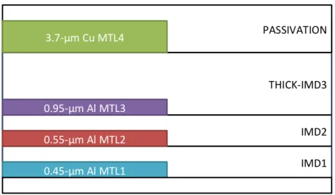
The key technology used in this work is a 0.35-µm SOI-BCD technology that fea-tures both 3.3 V and 5 V CMOS transistors, a 5 V VHF npn BJT, lateral pnp BJTs and several MOS devices providing high-voltage capabilities through drain-extension techniques [62]. Three Al metal layers with 0.45/0.55/0.9 µm thickness, respectively,
1.2 – Aim of this thesis
and a 3.7 µm-thick top Cu layer are available for routing. The process was enriched for this work by a thick-oxide module [63] that was previously developed and charac-terized for galvanic-isolated data transfer, similar to other state-of-the-art integrated isolators [9, 64, 65]. This module has been recently used for mass-production of sev-eral devices providing on-chip galvanic isolation [25, 42]. The thick oxide layer is located between the two top metal layers, as shown in the simplified back end of line (BEOL) cross-section in Fig. 1.16, and can have different thickness depending on the isolation rating. The technology choice was driven by its compatibility with the
Figure 1.16. Simplified cross-section of the available back end of line with thick oxide module for galvanic isolation.
thick-oxide module fabrication process and by the high resistivity of the available SOI substrate, that is mandatory to achieve high efficiency for power transformers6.
The second technology adopted in this work is a 0.13 µm standard CMOS pro-cess. Specifically, this technology was used to take advantage of the available high-voltage Schottky diode with sub-GHz operation capability, that has been a crucial
6It is worth noting that the SOI substrate is actually not required by the systems designed in
this work. In principle, as far as the substrate resistivity remains the same, same or better results can be achieved in a process with junction isolation, which also benefits from reduced thermal resistance.
element to implement an efficient power rectifier. All technologies were provided by STMicroelectronics.
1.2.3
Main results
Based on the discussion carried out in the previous section, three real-life applica-tions which require isolated power supplies and could immediately benefit from fully integrated power transfer systems were selected to be addressed during this work as a part of a research project at the RF-ADC, a joint research center between the University of Catania and STMicroelectronics. Accordingly, during my permanence at RF-ADC four fully-integrated systems were designed and characterized in the available technology by different design teams, showing measured performance that are competitive with the state of the art. They are:
• a watt-level, step-up, dc/dc converter for gate driver’s power supplies [66], • two medium-power CMOS converters, with output power of 200 mW and
300 mW, respectively, for power supplies of general purpose circuitry [5, 19], • a highly integrated data/power transfer system, with relatively low output
power, for sensor interfaces applications [17].
Gate drivers pose the highest challenges for silicon technology, since relatively high output power with output voltage around 20 V is required. Such high-power levels entails large area to comply with technology limits and hence its design was addressed to the optimization of power efficiency for a given area constraint, ex-ploiting high-voltage devices such as LDMOS transistors for this task, eventually.
General purpose circuitry, such as the aforementioned wireline transceivers and signal processing blocks, require lower output power and output voltages compared to gate drivers. For generic applications the reduction of technology costs is manda-tory to increase the appeal of these innovative integrated systems and hence new
1.2 – Aim of this thesis
topologies requiring only low-cost, widespread CMOS devices were introduced in [67] and demonstrated in [5, 19].
Finally, sensor interfaces require quite lower output power, e.g. around 10-20 mW, but the need for a data link typically leads to multiple isolation transformer, thus highly affecting the cost of these systems. A new architecture was proposed in [68], which enables both data and power transfer to be implemented with a single integrated isolation transformer, thus showing a great competitive advantage with respect to the state of the art.
Details of the implementations and measured results for some of these integrated systems are the object of this thesis. Specifically, I was in charge for the design and characterization of the watt-level converter presented in [66] and of the data receiver of the data/power transfer system demonstrated in [17], which will be thoroughly discussed in Chap. 2 and Chap. 3, respectively. For each system the design was focused on the maximization of power transfer performance, which is the key pa-rameter to understand the viability of the approach and, eventually, to determine if and which technology improvements are mandatory. Due to the lack of similar examples in literature, this activity has been a quite time-consuming task, which prevented other themes such as CMTI, thermal issues, and closed-loop control to be addressed. Further to the data receiver, the design was addressed to the maximiza-tion of robustness though novel topologies which guarantee wide operating range in terms of input signals.
Apart from these main activities, I also contributed to the implementation of the two CMOS converters with an innovative scalable lumped model [5] and by introducing the hybrid coupling for the topology adopted in [19]. These points are briefly discussed in App. B.
Chapter 2
A watt-level, step-up, power transfer
system
This chapter deals with the design and the experimental characterization of a watt-level step-up dc-dc converter for gate driver’s power supplies. The converter was designed to produce a 20-V output voltage, VOU T, from a 5-V power supply, VDD.
To enable a wide range of applications, a relatively high output power of 1 W was addressed. Consequently, the maximization of power density is of utmost importance to achieve a practical, cost-effective solution. An upper bound of 10 mm2was chosen
as a reasonable specification for the whole system area, which had a significant impact on the converter topology and design. Furthermore, the design was tailored to the maximization of power efficiency, which is another key aspect for practical implementation due to detrimental thermal effects and limited power dissipation of plastic packages.
2.1
System description
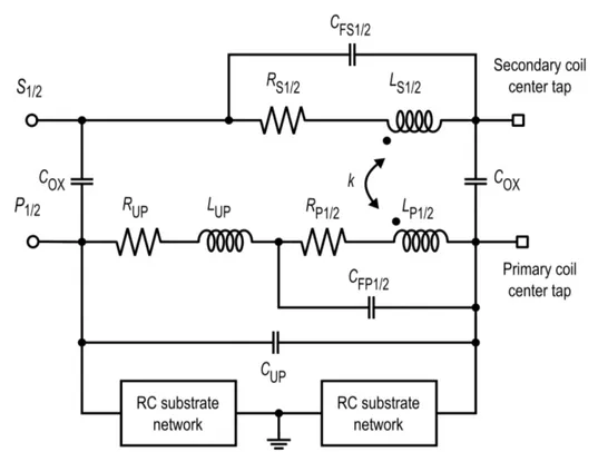
A simplified schematic of the galvanically isolated step-up converter is depicted in Fig. 2.1. The integrated transformer, TISO, is the core of the system since it performs
on-chip galvanic isolation and power transfer. In the proposed implementation it is integrated into the power oscillator chip, whereas a second die houses a full-bridge rectifier for ac-dc conversion, and the turn’s ratio of the transformer is exploited to achieve the required step-up voltage conversion ratio. The oscillator chip was fabricated in a 0.35-µm BCD technology providing on-chip galvanic isolation, while the rectifier was fabricated in a 0.13-µm standard CMOS technology, both described in Sec. 1.2.
2.1 – System description
The power oscillator adopts the transformer-loaded cross-coupled topology shown in Fig. 2.1, which is operated in class D to improve power efficiency. The need for highest power density dictates the choice of this topology that is the simplest differ-ential transformer-loaded oscillator: only a differdiffer-ential transformer and two power transistors are required to implement the dc-ac conversion. Differential operation was preferred because it minimizes the impact of bonding wires and other common-mode parasitics on the system, relaxes power constraints on the transformer coils, since each coil has to deal with half the dc current, and does not require complex feedback networks to implement the oscillator, which would be the case for a single-ended topology. Simplicity maximizes the converter’s power density by reducing the number of transistors and passive components, although it entails several com-promises between each building blocks, which make the design optimization a quite complex problem. For example, the isolation transformer has to implement isolated power transfer while working as a resonating tank for the active oscillator core, i.e. M1,2 and the relative bias network. Similar issues arise with the oscillator active
core, which must provide the non-linear reactance required to sustain the oscillation and enough power at the transformer primary coils, but it is affected by parasitic capacitances which reduce transformer efficiency. Moreover, the converter operation is similar to the push-pull or flyback converter, which is indicated in [55] as one of the most promising topology for fully integration of galvanic isolated converters.
This topology clearly requires active devices able to sustain at least two times the supply voltage and at the same time operate at very high frequency (VHF). LDMOS transistors similar to [62], available in the adopted BCD process, were used for M1,2. Being asymmetric devices, their maximum allowed gate-source voltage,
VGS,M AX, is smaller than the maximum drain-gate voltage VDG,M AX, and hence
capacitive coupling is exploited to avoid gate-oxide breakdown. Indeed, coupling capacitors CB1/2 perform a voltage partition with the gate capacitance of M1/2, thus
They were implemented with 12-V poly-poly capacitors. The transformer is modeled with coupled inductors, LP 1,2 and LS1,2, that represent the primary and secondary
coils, respectively. It is worth noting that LP 1,2 resonates with the large parasitic
capacitance at the oscillator drains, VD1,2, to maximize the oscillation frequency
fOSC and hence the efficiency of the transformer. Finally, a turn-off circuitry is
added to switch off the cross-coupled pair. It consists of a network of NMOS switches connected between the gate of the M1,2 and ground. A tree of buffers ensures that
all the power cells are switched off reliably and almost simultaneously. The turn-off control circuitry is used to control the output power of the converter by periodically switching-off the oscillator. The VHF operating frequency actually simplifies the control of the output power without affecting power efficiency (e.g., PWM or PFM modulations) [55, 56, 58, 59, 60, 61]. Indeed, when the power oscillator is on, it operates at the maximum output power and hence with maximum efficiency, and when is off only leakage current is drawn.
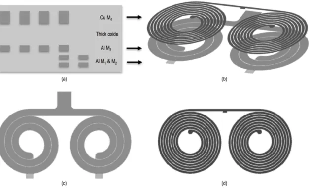
A stacked configuration is used for the transformer, exploiting standard metal 3 and metal 4 for primary and secondary windings, respectively, while the lowest two metals are shunted and used for underpasses, as shown in Fig. 2.2, to minimize their series resistance. The differential topology adopted for the oscillator would suggest the use of a fully symmetric, differential, spiral configuration for the transformer. Such configuration maximizes the quality factor and reduces the area occupation of the coils but requires two underpasses at least for each inductor turn. Therefore, it is not a viable solution for power transfer applications in the adopted technology, because of the higher parasitic capacitance and series resistance of this topology. In-stead, two stacked transformers were preferred, which require only two underpasses, thus simplifying the layout. A distance higher than 70 µm was found to guarantee negligible coupling effects between right and left sides of the transformer, as reported in literature [69]. Of course, high coupling factor between primary and secondary coils is mandatory for an optimized design since a low k-factor combined with the
2.1 – System description
Figure 2.2. Simplified layout of the isolation transformer: (a) BEOL cross-section, (b) 3-D view of the transformer, (c) planar view of the primary coils, and (d) planar view of the secondary coils.
poor Q-factor of integrated transformers would highly affect the power transfer ef-ficiency. Consequently, the maximization of the overlap area between primary and secondary windings is crucial to avoid magnetic coupling factor degradation [70]. Since a high transformer turn’s ratio must be used to step-up the output voltage, a proper relationship between primary and secondary geometrical parameters is re-quired to maximize winding overlap, and it was taken into account at the design time. At the secondary side, two bonding wires are used for the connection towards the rectifier chip. The impact of these bonding wires on the system performance is negligible since they are connected in series with the high inductance of LS1,2.
2.2
Efficiency analysis and design issues
The design of this dc-dc converter poses several challenges since it is characterized by non-linear interactions between each building stage, which involve system opti-mization if the maximum efficiency must be addressed. Although radio-frequency (RF) class-D oscillators have recently gained attention for their excellent efficiency in highly scaled technologies, most recent literature focuses on phase noise and power consumption optimization [71, 72], whereas the design for power transfer applica-tions is a quite different problem.
In this section we analyze how each block efficiency depends on the design pa-rameters of the converter as well as on the loading effect of the other blocks, to better understand main issues and trade-offs between each building block design. The overall system efficiency, η, is the product of the efficiency of each building block when operated into the whole system. Specifically, the power flow from the power supply, PDD, to the dc power delivered to the load, POU T, involves losses in the
active devices, in the integrated transformer, and in the rectifier, as detailed in the flow diagram of Fig. 2.3. Here PT X is the total power at the transformer input coils,
Figure 2.3. Power transfer flow diagram.
and POU T_AC is the ac power at the transformer output. The rectifier efficiency,
ηRECT, is defined as POU T/POU T_AC, while the overall efficiency of the transformer,
![Table 1.2. System-level standards involving isolation by market and region [4].](https://thumb-eu.123doks.com/thumbv2/123dokorg/4504516.34234/24.892.94.735.639.737/table-level-standards-involving-isolation-market-region.webp)