Analysis of the near-intrinsic and extrinsic photocapacDtance due to the
El2
level in boron implanted GaAs
J.
R. Morante, J. Samitier, A. Perez, and H. AltelarreaCatedra d'Electrimica. Facultat de Ffsica, Universitat de Barcelona. Diagonal 645. Barcelona 08028, Spain S. Gourrier
Laboratoires d'Electronique et de Physique Appliquee, LEP a) 3, avenue Descartes, 94450 Limeil-Brevannes. France
(Received 24 February 1986; accepted for publication 20 May 1986)
A detailed analysis of the photocapacitance signal at the near-band and extrinsic energetic ranges in Schottky barriers obtained on horizontal Bridgman GaAs wafers, which were implanted with boron at different doses and annealed at several temperatures, has been carried out by using the optical isothermal transient spectroscopy, OITS. The opticai cross sections have been determined as well as the quenching efficiency of the EL21eve1 which has been found to be independent of the annealing temperature. Moreover, the quenching relaxation presents two significant features: (i) a strong increase of the quenching efficiency from 1.35 eV on and (ii) a diminution of the quenching transient amplitude in relation with that shown by the fundamental EL21evel. In order to explain this behavior, different cases are discussed assuming the presence of several energy levels, the existence of an optical recuperation, or the association of the EL2 trap with two levels located, respectively, atEv
+
0.45 eV and Ee - 0.75 eV. The theoretical simulation, taking into account these two last cases, is in agreement with the experimental photocapacitance data at low temperature, as well as at room temperature where the EL2 filling phototransient shows an anomalous behavior. Moreover, unlike the previous data reported for the EL2 electron optical cross section, the values found using our experimental technique are in agreement with the behavior deduced from the theoretical calculation. The utilization of the OITS method has also allowed the determination of another level, whose faster optical contribution is often added to that of the EL2 level when the DLOS or standard photocapacitance is used.INTRODUCTION
The midgap EL21eve1 at Ee - 0.75 eV, is created by a native donor defect in GaAs except when it is grown by LPE. It can also be created by means of plastic deformation, ionic implantation, or neutron irradiation. In these cases, the DLTS (deep level transient spectroscopy) spectra of the un-treated samples do not show the normal peak corresponding to the EL2 center, but they show the presence of the Uband. It is necessary to anneal at temperatures higher than 450 ·C to obtain the EL2 peak in the DLTS spectra. I Initially, this
was explained assuming that the formation of the EL2 center does not occur below such temperatures. On the contrary, several recent works have reported the association between the EL6 and EL2 native defects, in order to justify the origin of the Uband and to prove the direct EL2 creation by means of those processes. Moreover, this allows us to reconcile again the EL2 level with the data obtained from EPR (elec-tronic paramagnetic resonance), attributed to the ASOa de-fect.2•3 Nevertheless, considering theoretical calculations, this antisite appears as a double charge donor, whose higher energy state would be the EL2 level and whose second level has recently been identified by Wosinski4 and Lagowski et a/.,s as a level located at about 0.5 eV above the top of the valence band.
The main characteristic of the EL2 level is the quench-ing of its photoresponse. The fundamental EL2 level relaxes
a) LEP. a member of the Philips Research Organization.
to a new state, labeled EL2 metastable state, which does not show the optical response. This photoelectric fatigue or quenching has been analyzed by Vincent et al.6 These auth-ors reported that quenching efficiency begins at about 0.9 e V, passes through a maximum located at about 1.12 e V and goes to zero before reaching 1.35 eV. More recently, Tanigu-chi and Ikoma 7 have carried out measurements which indi-cate further increases of the quenching efficiency from about 1.35 eV, depending on the samples used.
The fundamental EL2 state can again be recuperated in a thermal or electrical way. Thus, when the light is off, the unquenched state can be recuperated with a temperature de-pendent rate. This thermal recuperation is consistent with a single diffusion like atomic displacement process. Alternati-vely to the thermal recuperation, the presence of free elec-trons gives rise to the electrical recuperation of the un-quenched states.
The existence of an excited state near the conduction band, or the participation of a donor shallow level in the process, has been claimed8 in order to explain this last
mech-anism. Likewise, several works have reported experimental data which suggest such a possibility. Shanabrook9 found that the above gap excitation photoluminescence spectra ex-hibit an oscillatory behavior, which is attributed to resonant cooling of hot electrons by emission of LO phonons. This indicates that the energy transfer or capture process is domi-nated by a shallow donor state, whose capture cross section is sensitive to the free electron energy before capture. Analo-1661 J. Appl. Phys. 60 (5).1 September 1986 0021-8979/86/171661-09$02.40 @ 1986 American Institute of Physics 1661
gous results have been found by Leyral et al. 10 Recently Ji-menez et a/. 11 have found that, after excitation with photons of about 1.15 eV, another quenching phenomenon takes place, which is the optical quenching of the photocurrent in the near band-edge spectral region. It has been explained on the basis ofa two-step mechanism: (i) the EL2level electro-statically associates with shallow levels, when it is optically ionized at low temperatures; (ii) afterwards the shallow lev-el rlev-elaxes to a quenched state. Furthermore, Nojimal2 has reported the existence of an optical slow-relaxation phenom-enon, or a slow optical fatigue in the photoconductivity mea-surements on undoped semi-insulating liquid encapsulated Czochralski GaAs, which has been attributed to an optical transition from the quenched to the fundamental EL2 state. In the present paper, we report the experimental results of the near-band and extrinsic photocapacitance related with the EL2 level. The measurements were obtained from the new method, labeled OITS, recently reported3 which allows a more spectroscopic analysis of the photocapacitance sig-nals than the standard photocapacitance or DLOS tech-niques. The analyzed samples were Au:GaAs Schottky bar-riers which were boron implanted at different doses and, afterwards, annealed at different temperatures. The data analysis carried out has allowed us to do the following:
( 1) to explain both the increase of the quenching effi-ciency and the diminution of the expected EL2 quenching amplitude, at energies greater than about 1.2 eV;
( 2) to deduce the exact EL2 electron optical cross sec-tion,
£f,:
in the near-band energetic range which, unlike the data previously reported by other authors, 13 has been found to show a good agreement with the results of its theoretical calculation;(3) to identify the presence of another level whose opti-cal response appears to be mixed with the EL2 level one;
( 4) to show that the EL2 quenching efficiency and opti-cal cross sections are independent of the annealing tempera-ture;
(5) on the basis of the above results, to report a model assuming an optical recuperation between the metastable and fundamental states and the presence of a second level associated with the EL2 center. This level. would be located at about 0.45 eV above the valence band, according to the values previously proposed by W osinski4 and Lagowski
ef
a/. s The kinetic equations developed from this model
con-firm the experimental results found at low temperatures, as wen as the anomalous photocapacitance behavior at room temperature.
EXPERIMENT
The measured samples were obtained using, as starting material, horizontal Bridgman n-GaAs with a free electron concentration of about 8 X 1016 cm
-3. The polished surface Was capped with a
lOoo-A
CVD Si3N41.ayer and annealed at 870·C for 15 min in order to decrease the native electron trap concentration in a I-Ilm-thick layer below the surface. After removing the Si3N4 capping layer, the samples were implanted with boron except for the testing sample. The dose was 1010 and. 1011 ions/cm3 and the ion kinetic energy 100 keY. The annealing treatments were carried out in an1662 J. Appl. Phys., Vol. 60, No.5, 1 September 1986
open furnace, using the close-contact technique under Hz
flux during 15 min at a temperature range between 300 and 800 ·C. Finally, the Schottky diodes were obtained by eva-porating gold electrodes on the surface ofthe implanted and nonimplanted samples.
The defect concentration for the boron dose used is ade-quately small to faciJ.itate the capacitance transients inter-pretation. However, we find a strong nonexponentiaJ photo-capacitance response. Its analysis presents a greater difficulty than in the usual case. This is due to the addition of exponential transients of different levels whose optical re-sponse, concentration, and optical cross sections are not well known a priori. Accordingly, the standard photocapacitance and the DLOS experimental techniques6 are rather unsuita-ble for characterizing the samples with possiunsuita-ble nonexpon-ential transients.
We have used a new experimental method based on the time analysis of the isothermal phototransients (optical iso-thermal transient spectroscopy). 3 Once the phototransient is stored in the computer and normalized to its initial value, the aITS signal is generated by sampling the photocapaci-tance at different times f, and f,K, where K> I is a fixed parameter. For each f" the OITS signal is
Set, ,jl{,
n
= [C(t,K) - C(ti) ]/In(K). (1)For each level with optical response, straightforward calcu-lations show the existence of a maximum of the OITS signal. These maxima are characterized by their height Hmax and their position at the time logarithm axis fmax , which are giv-en, respectively, by
H
e~
NT K - 1 K - K / ( K - I ) , (2a. )ma,,=o 02 I
en +ep ND nK
fmax =
(e~
+
e~)
- I ,jl{ln K, (2b)K-I
where e~ and e~ are the electron and hole optical emission coefficients, NTis the trap level concentration, and No the shallow donor density. From these equations, when the mi-nority optical emission coefficient is smaller than that of the majority carriers, the level concentration and the majority optical emission can be directly deduced. In the other cases, one can only obtain a magnitude proportional to the major-ity optical. emission coefficient and the concentration at a fixed photon energy.
Figure I shows representative photocapacitance tran-sients together with their OITS spectrum at low tempera-tures, T = 80 K, for two samples annealed at different tem-peratures. The dashed lines correspond to the fitting, assuming the addition of different exponential transients. Figure 2 shows the experimental setup which is the standard one used for the photocapacitance measurements.
RESULTS
The DLTS spectra of our samples show the existence of the EL6 and EL2levels together with the Uband, Fig. 3. As the annealing temperature increases the EL6 and U-band concentrations become smaller, being negligible from 500 ·C on. Then, the DL TS spectra show only the EL2 peak.
l:1C C(a.u.)
C(pF)
3 197 195 193 0 6 195 2 o 190 -2~~~~ __ ~~ __ ~ __ ~ 10- 2 10-' 10° 10' 10 2 t(s)FIG. I. OITS spectra at different excitation energies and annealing tem-peratures. The thick lines are, respectively, the photocapacitance transients.
fore, we have used basically the samples annealed at a tem-perature of 600 ·C for the photocapacitance measurements of the EL2 leveL
Figure 4 shows a photocapacitance transient obtained from the sample annealed at 600 ·C and its corresponding OITS spectrum, together with other OITS spectra at differ-ent annealing temperatures with an illumination energy of
1.44 e V. The dashed line represents the theoretical fitting of the 6OO·C aITS spectrum, assuming the superposition of two exponentials. It should be noted that at this photon ener-gy, the samples annealed at temperatures greater than 475·C show a new peak, which we have named P peak. In Fig. 5 we show aITS spectra at different photon energies for
MONO-CHROMATOR
CAPACI-METER BOONTON
FIG. 2. Experimental setup.
COMPUTER
1663 J. Appl. Phys., Vol. 60. No.5, 1 September 1986
l:1C/C x 103 6 11 =O.lseg 12=15<'9 5 4 3 2 a 150 200 250 300 350 T (OK)
FIG. 3. DLTS spectra of the gold Schottky barriers obtained on the hori-zontal Bridgman GaAs afterwards implanted with boron and annealed at different temperatures.
the samples annealed at 6OO.C. In Fig. 6 we present the quenching efficiency versus the photon energy. These values have been deduced from each aITS spectrum according to Eqs. (2a) and (2b). The dashed line corresponds to values reported by Vincent et al.6
Several points about the negative quenching peak Q should be noted:
(i) The quenching efficiency increases from 1.35 eV (Fig. 6).
(ii) Its amplitude is much smaller than that measured in the usual quenching range, where the amplitude of the Q and M peaks are equal when the recuperation is negligible in front of the quenching efficiency.6 This behavior begins at
AC
C.-________________________
C(pF) ~ AU PEAK P T=80K hv="44eV t(s)FIG. 4. OITS spectra at different annealing temperatures with hv = 1.44 eV. The thick line corresponds to photocapacitance transient of the sample annealed at 600 ·C and the dashed line is the litting carried out assuming the contribution of several exponential transients.
I!.C
C
PEAK P T :600'C hv 10 1.46~Y 1.4 eY A.U. 1.3 eY 1.2 eY 1.1 eY 5FIG. 5. alTS spectra at different photon energies for the samples annealed at T A = 600 'c.
about 1.2 eV and becomes larger in the near intrinsic region, as is shown in Fig. 7.
A similar increase of the quenching efficiency from about 1.35 eV has also been reported by Taniguchi et aU Their samples were obtained from different technological processes or subjected to implantation. They assumed the existence of a multilevel family associated with EL2 level.
The P peak level has never been noticed by DLTS or DLOS. Its optical response begins to be detected at about
1.5 >- A.U. u
z
!:!:! u IJ... IJ... L&J C!)z
:I: u ~ 05 :::)"
PNk Q T=80K'/-.\
..
.
\ I \ ./ \'I
I \ I \ /. ! t\ I j • \ I \/
t\
I \ 0 I. .\ d ~ / 'I. T. =350'C T. =400"C • T. =475'C • T.=600·C,
,
...
.... I 0~----~~----~---~---~----7, 1 11 12 13 14 15 hY(~V)FIG. 6. Quenching efficiency for the Schottky diodes obtained on boron implanted GaAs at 1010 ions/cm2 having 100 ke V of energy and at different annealing temperatures. The dashed line corresponds to the values found by Vincent et al.6
1664 J. Appl. Phys .• Vol. 60. No.5. 1 September 1986
H/vI/Ha 5 4 3 2 o~ ____ ~ ______ ~ ____ ~ ______ ~ ____ ~ 1.1 1.2 1.3 1.4 1.5 hv(eV)
FIG. 7. Amplitude ratio of the EL2 and quenching aITS peaks.
1.15 e V and can be exactly separated from the M peak contri-bution by the OITS method from 1.28 eV.
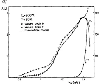
In Fig. 8 we present the electron optical cross-section values, deduced from theM and Ppeaks with the same arbi-trary units. We attribute the M peak to the EL2 level, ac-cording to the behavior of its optical cross section with the photon energy. The dashed line corresponds to the theoreti-cal model of Chantre14
and the crosses are the values pre-viously reported by other authors.6
•12 Figure 9 shows the M
peak ~ versus the photon energy for different annealing temperatures. The observed variation has been attributed to the interaction between the EL2 and the EL6 levels analyzed elsewhere. 3 J~ikewise, the EL2 ~ values have been deduced from theOITS spectra, taking into account theN T / No ratio
deduced by meanS of the DLTS spectra. The obtained data present an increase after energies greater than 1.3 eV, Fig.
to.
whose theoretical fitting excludes any possibility of its being due to the transition between ther
7 valence bandmax-imum and the El~2 level. Moreover. our values and. those
A.U.
T.=600·C T=80K • valu~ peak /vi A vailIt'S peak P ___ thl'orl'tical modl'l 0.8 150 100 12 hv(eV)
FIG. 8. Electron optical cross section of the M peak attributed to EL2 level vs the photon energy measured using the sample annealed at T" = 600 ·C.
The dashed line is the theoretical model and the symbols ( X ) are the ex· perimental values according to Refs. 6 and 13. The triangles are the electron optical cross section associated with the peak P eJlpressed with the same units.
O"~{Q.U.) 2 Q8 1.2 haOK peakM 14 hv{eV)
FIG. 9. Electron optical cross section of the M peak attributed to the EL2 level vs the photon energy taking the annealing temperature as a parameter. found in previous work at different temperatures 14 suggest that the ~ increase is caused by the absorption due to the presence of another donor level D associated with the EL2 center. This level would be the associated state located near the conduction-band maximum which has been determined from photoluminescence excitation measurements9•10 or Hall measurements. 15
Also, it must be noted that the O'~ data present a diminu-tion from about 1.4 eV, in agreement with the theoretical calculation. The previously reported values deduced from DLOS do not show this diminution. However, it has been pointed out from photoluminescence measurements. 9. 10 We think that this disagreement is due to the presence of the P
peak whose contribution cannot be separated using the DLOS method, but it can be measured correctly using our OrTS method. 3 This strong diminution, together with the ~ increase, contributes to increase the quenching efficiency ac-cording to its expression deduced from the Vincent et al. mode1.6 It should be noted that the increase of ~ must de-pend on the origin of the D defect. This would explain the different values of the quenching efficiency obtained in sam-ples from different starting materials.
A.U
•
•
0.8 PEAK M T=80K.
..
.-
..
.
.
•
•
• •
•
1.2•
•
•
•
....
1.4 hll(eV)FIG. 10. Hole optical cross section of the M peak attributed to EL21evel vs the photon energy.
1665 J. Appl. Phys .• Vol. 60, No.5, 1 September 1986
DISCUSSION
The presence of this P peak brings about the question of its origin. WosinskV and more recently Lagowski et al.,5 have reported the existence of a level located at about 0.45 e V above the valence band, which was attributed to a paramag-netic state of the Asi.: while the usual EL2 level should be
the nonparamagnetic state Asb:. 16 However, a detailed
analysis of the EL2 andPconcentrations at different anneal-ing temperatures, Fig. 4, allows us to reject the possibility that the P peak is due to the level found by Wosinski or Lagowski et al. Our experimental data rather suggest that
the P peak appears with the annealing process in a different
way than the EL2 level. This peak might be related to the defects created by the boron implantation, BAS or GaAs , as
reported by Dansas.17
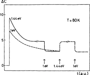
Interesting features about the photocapacitance behav-ior appear when the energy of the illumination is changed. Figures 11 and 12 show the evolution of the photocapaci-tance versus the time, under the consecutive illumination with photons of different energies. The final value of the photocapacitance does not show any dependence on the al· temative order of the illumination. Thus, the change of the photon energy gives rise to a sudden photocapacitance vari-ation which is followed by a slower relaxvari-ation. These fea-tures can be summarized as follows:
(i) The photocapacitance variations caused by the change of the illumination energy are steplike. This is due to the photocapacitance being related to the sum of the popula-tions of electrons at levels related with the EL2, or other center. In the photocurrent case, the illumination change should give a spikelike variation which is in agreement with the previous work of Jimenez et al. II and Nojima. 12 Like the results of these authors, the photocapacitance step depends on the application time of the second illumination, i.e., de-pends on the EL2 occupancy.
(ii) The switch-off illumination after reaching the steady value of the photocapacitance gives rise to a transient, but the following illumination with photons of energy hv
regenerates, again, the steady value for this energy.
(iii) The steplike photocapacitance variation shows two
hoC 10 T=80K 5 ""'" O
j
l ... ,...=L
('->','--,'----_
I
i
-- - ---.l L _i i i
1 e>J 1.44eV leVt (a.u.)
FIG. II. Experimental evolution of the photocapacitance correspOnding to the application, consecutively, of different photon energies.
6.C
13geV 15 10 5 / t (a.u.)FIG. 12. Experimental evolution of the photocapacitance corresponding to the application, consecutively, of different photon energies.
components, fast and slow, which depend on the illumina-tion energy.
The existence of these two different relaxation processes suggests that there are two mechanisms. On the one hand, given the large values of the electron optical. cross section of the P level, it is reasonable to think that the fast variation of the photocapacitance can partially be due to the contribu-tion of this level. On the other hand, the only contribution of the EL2 level cannot explain the slow relaxation, unless the metastable EL2 shows an optical response. We have two options to explain the second mechanism:
(i) There is another level X which generates the slow relaxation.
(ii) The metastable EL21evel presents optical response. In the first case, the time constants associated with theX level should correspond to the quenching efficiency to justify the diminution of its expected amplitude in relation with that of the EL2 peak in the OITS spectra. Moreover, this amplitude should be similar to that of the EL2 to explain the quasi-extinction of the quenching. Thus, under these condi-tions, once all the EL2 center are in the metastable state, the photocapacitance changes would be only due to the X level. In the second case, the optical response of the metasta-ble EL2 level leads to two new possibilities:
(a) The existence of a direct optical recuperation pro-cess;
(b) The existence of a second level. associated with the EL2 center together with the optical recuperation process, on the basis of the results of the Wosinsky4 and Lagowski et al.5
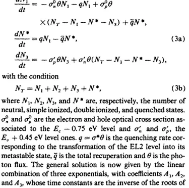
Both possibilities can be analyzed together taking into account that the first one is a particular case of the second one, assuming null values for the second l.evel optical cross sections. Thus, in the (b) case, we can suppose that the EL2 level corresponds to the neutral charge state which presents a first ionization energy threshold about 0.75 eV and a sec-ond about 1.05 eV. Therefore, according to this assumption, the new kinetic equations governing the persistent photoca-pacitance quenching become
1666 J. Appl. Phys., Vol. 60, No.5, 1 September 1986
dNI = _ d!.()NI - qNJ
+
d!.() dt n p X(NT -NI-N* -N3) +qN*, dN* --=qNI-qN*, (3a) dt dN3 () - - = - 0';()N3+
O'~ (NT - N} - N* - N3 ), dtwith the condition
NT =NI +N2 +N)+N*, (3b)
where NI • N2 , N3 , and N
*
are, respectively, the number ofneutral, simple ionized, double ionized, and quenched states.
~ and ~ are the electron and hole optical cross section as-sociated to the Ee - 0.75 eV level and O'~ and 0';, the
Ev
+
0.45 eV level ones. q = O'*() is the quenching rate cor-responding to the transformation of the EL2 level into its metastable state,q
is the total recuperation and () is the pho-ton fiux. The general solution is now given by the linear combination of three exponentials, with coefficients A I ' A2,and A 3' whose time constants are the inverse of the roots of the following equation:
0= A 3
+
[q+
q+
(~+
~+
O'~+
O';)() JA 2+
[(~()+
q+
~()q+
q(~() -q)
+ (O'~ +O';)()(q+q+~e+~() -0'~~e2]A
+ a;e [(~
+
~)eq +q~e]+
~~e2q. (4)Under illumination. the steady-state value of the posi-tive charge can be expressed by
d!. 0" e 2q- - d!. 0" () 2(q
+
q-) P( 00) = 1+
n n p pO';()(~
+
~)eq+
q~()+
~0';()2q(5)
According to the value ofq
the values of P( 00 ) can change from zero, for'ii
= 0, to0" d!. - 0" d!. P( 00 )
=
1 +
n n p p(~
+
~ )0';+
O'~d.:(6)
for 'ii-infinite. It should be noted that O'~ also acts exactly as a recuperation process; the smaner the 0'; is, the more effec-tive the process will be.
Taking into account the values ofthe optical cross sec-tion, as well as those of the quenching efficiency and optical recuperation that will be used later to carry out the fitting of the experimental photocapacitance, the solutions of Eq. (4)
can approximately be given by AI::::
(d.:
+
~)(),
A2::::(0'~ +O';}(), (7)
O';[(~ +~)q+q~] +O'~~q
A3:::: .
(O'~
+
O';)(~ +~)UsuaUy, A2 is larger than AI' but the amplitude of the associated exponential A2 is negligible. Moreover, A3 and the amplitude A3 show a direct dependence on the optical pa-rameters. The increase of ~ and
q.
and the diminution of ~ give rise to an increase of the quenching efficiency.C{a.u.)
<i=
-::;;;~==================tO
r
0.1-~=;;;:;:;:;;;:::----_0.D1
3 5 7 0.001 0.0001 9t
(a.uJ
FIG. 13. Theoretical photocapacitance transients calculated from the mod-el of a second ionization levmod-el for the EL2 center assuming different values of recuperation from the metastable state to the fundamental state.
d.:
= ~=
1 a.u., (J"*=
10-2 a.u., (J"~=
10-3 a.u., and 0;. = 10-1 a.u.Figure 13 shows the numerical calculation of the above kinetic equation for different values of the recuperation
q,
assuming thatd.:
= ~=
1, u~ = 0.001,u;
=
0.Q1, and u*=
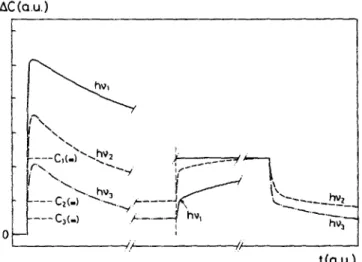
10-2 a.u. Recuperation values as small as qll0 are enough to give rise to the diminution of the quenching ampli-tude.The numerical simulation of the consecutive application of two photon energies is shown in Fig. 14. We have also included the variation due to the P level, according to the amplitude variation of the P peak in the OJTS spectra. The qualitative agreement \1.'ith the experimental results is excel· lent. Thus, this model allows us to explain the detailed
be-havior of the photoca.pacitanee.
On the contrary, the possible existence of other levels, besides the P level, which could also justify the photocapaci-tance variations, has not been corroborated. The analysis of the OITS spectra at temperatures where the thermal recu-peration is larger than the quenching efficiency does not show any time constant in the quenching efficiency range with enough amplitude to justify the quenching reduction.
6.C (a.u.)
FIG. 14. Theoretical simulation of the experimental measurements shown in Fig. 10.
1667 J. AppJ. Phys" Vol. 60, No.5, 1 September 1986
H (a.u.) 4 3 2
o
••• EXPERIMENTAL - THEORETICALZ(s)
FIG. 15. OITS spectra of the photocapacitance transient carried out at
T = 140 K with hv = 1.18 e V using the sample annealed at 6OO'C. The continuous line is the theoretical fitting using three time constants and the dots correspond to the experimental photocapacitance transient.
This can be seen in Fig. 15, which shows the OITS spectra of a photocapacitance transient at 140K. It does not appear any level of amplitude comparable to that of the EL2 level. The theoretical fitting has been realized using three time con-stants of 10.7, 165.4, and 708.9 s with amplitudes, respective-ly, of 0.16, 4.2, and 0.9 a.u. We have assumed a smooth dependence on the temperature of the optical cross sections of every level. Moreover, neither the illumination with pho-ton energy of about 0.67 eV, nor the annealing at tempera-tures greater than 700 ·C, where the EL2 concentration be-comes negligible, have led to the identification of residual levels with concentration and optical parameters suitable to explain the experimental data. The residual leve1s show a concentration smaller than 1015 cm-3
•
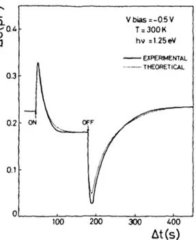
Besides the photocapacitance behavior at low tempera-tures, there is another interesting feature whkh indicates the contribution of the second level associated ... ~:ith the EL2 cen-ter. It appears at room temperature, when all the EL2 centers have been thermally emptied and the t~ample is illu-minated with a photon energy greater than about 1 eV. The photocapacitance initially increases; afte~ards it deere.ases towards its steady value which agrees With that obtamed from the initial condition with all the EL2 centers filled, Fig.
16. The thermal recuperation of the steady value in darkness shows also a special evolution. First, the capacitance rapidly diminishes. Then, it increases with a slower relaxation. This situation can also be simulated by means of the above model, dashed line in Fig. 16.
Moreover, in the case of all the EL2 centers being full, the model gives an only exponential transient. The ampli-tudes associated with the other time constants are negligible. Thus, in spite of the three time constants involved according to the model, the experimental EL2 emptied phototransients are found to be exponential. On the contrary, in the case of the existence of other levels, the emptied phototransient should be clearly nonexponential. The good accordance con-firms the existence of the second level associated with the EL2 center. Similar behavior has been found in the samples Morante et al. 1667
I
I
I Ii
\.~
\
Ii
... lL..a.
... 0.4 U <] 0.3 0.2 0.1 OFF V bias =-0.5 V T = 300K hll :1.25eV - - EXPERIMENTAL ... - ... THEORETICAL ... ~ ... . O~ __ ~~ ____ ~~ __ ~~ __ ~~~ 100 200 300 4006t(s)
FIG. 16. Photocapacitance transient at room temperature with a photon energy hv = 1.25 eV. The dots are the theoretical fitting according to the developed model.
obtained on the nonirnplanted material and whose DLTS spectra show only the EL2 peak. We think that the small difference between the experimental and theoretical curves is due to the ionization of other hole traps. The developed analysis corroborates that this behavior is an intrinsic char-acteristic of the EL2 center and does not depend on other levels with optical response, as the P level.
CONCLUSION
In conclusion, from the OrTS analysis of the near-band and extrinsic photocapacitance of the boron implanted GaAs Schottky barriers, annealed at several temperatures, we have shown that in the samples annealed at 600 ·C, where there is no contribution of the EL6 level, besides the EL2 center, there are other two levels with optical response: (i)
the P level, (ii) the second level associated with the EL2 center.
The P labeled level shows an optical electron cross
sec-tion greater than that of the EL2 center, which has exactly been deduced, solving the apparent incompatibility between its theoretical model and the DLOS data previously reported for values greater than 1.39 eV. The concentration of this P
level has been found to increase with the annealing tempera-ture. We think that it may be due to the BAs or GaAs accord-ing to the data reported by Dansas,17 Bishop et al.,18 and Elliot et al. 19
The other level, located. about
Ee -
1.05 eV, has been assumed in order to explain the inequality between the EL2 and quenching peak amplitude, on the basis of our experi-mental results and those ofWosinsky4 and Lagowski etaU
The devel.oped model has all.owed. us to explain the evolution of the photocapacitance transients as well as its behavior even at room temperature. The most significant feature of the developed mode! is the verification, using capacitance technique, of the optical recuperation previously reported by 1668 J. Appl. Phys., Vol. 60, No.5, 1 September 1986
Najima,'2 from photocurrent measurements. The distinc-tion between the effects originated by the presence of a level as the X level or the second level associated with the EL2 center is not straightforward. However, the confirmation of the double donor character of the EL2 center would necessi-tate a revision of the measurements previously carried out about the EL2 level.
On the other hand, we have not found any dependence on the annealing temperature of the EL2 optical parameters which have been measured using the OITS technique. The quenching efficiency increase found from 1.35 eV, has been explained taking into account the variation of the
d;:
and ~values corresponding to the EL2 level and the developed model. Also, the disagreement between the previous data reported by other authors and the theoretical model of the
d.:
has been eliminated by introducing the separation of the contributions of each level obtained using theons
instead of standard photocapacitance or DLOS.However, in spite of the agreement between the model developed and the experimental results, more experimental details are necessary, especially the use of different starting GaAs materials and processes, in order to obtain an exact assessment of the electrical and optical properties of the EL2 center. Neverthel.ess, the results reported are in agreement with those recently reported by J. Lagowski et al.5 usingp-type bulk GaAs.
ACKNOWLEDGMENTS
This work has been supported by French-Spanish coop-eration programme, CIRIT (Comissi6 Interdepartamental de Recerca i Innovacio Tecnologica) and CAICYT (Comis-ion Asesora de Investigaci6n Cientifica y Tecnol.ogica) pro-ject No. 2340/82. The authors would like to express their thanks to Dr. A. Herms and J. A. Anton for their helpful discussion.
'T. Ikoma, M. Takikawa, and M. Taniguchi, Inst. Phys. Conf. Ser. 63,191 (1982).
2G. M. Martin, E. Esteve, P. Langlade, and S. Makram-Ebeid, 1. Appl. Phys. 56, 2655 (1984).
3J. Samitier, J. R. Morante, L. Giraudet, and S. Gourrier, Appl. Phys. Lett.
48,1138 (1986).
"T. Wosinsky, Appl. Phys. A 36, 213 (1985).
'J. Lagowski, D. G. Lin, T. P. Chen, M. Skowronski, and H. C. Gatos, AppJ. Phys. Lett. 47,929 (1985).
6G. Vincent, D. Bois, and A. Chantree, J. Appl. Phys. 53, 3643 (1982). 7M. Taniguchi and T. Ikoma, AppJ. Phys. Lett. 45, 69 ( 1984). 8M. Levinson, Phys. Rev. B 28, 3660 (1983).
9JJ. V. Shanabrook, P. B. Klein, E. M. Swiggard, and S. G. Bishop, J. Appl. Phys. 54,336 (I983).
lOp. Leyral and G. Guillot, in Semi-Insulating III-V Materials. edited by
Makram-Ebeid and B. Tuck (Shiva Ltd., London, 1982), p. 166.
II}. Jimenez, P. Hernandez, J. A. Saja, and J. Bonnafe, J. Appl. Phys. 57, 5290 (1985).
12S. Nojima, J. Appl. Phys. 58, 3485 (I985).
I3A. Chantre, G. Vincent, and D. Bois, Phys. Rev. B 23,5335 (1981).
I4A. Chantre, These, Institute National des Sciences ApJiquees (INSA) Lyon, 1982.
ISW. Walukiewicz, 1. Lagowski, and H. C. Gatos, Appl. Phys. Lett. 43, 112 ( 1983).
1669 J. Appl. Phys., Vol. 50, No.5, 1 September 1986
16E. R. Weber, H. Ennen, U. Kaufmann, J. Windscheif, J. Schneider, and T. Wosinski, I. Appl. Phys. 53, 6140 (1982).
17p. Dansas, I. Appl. Phys. 58, 2212 (1985).
18S. G. Bishop, B. V. Shanabrook, and W. J. Moore, J. Appl. Phys. 56, 1785 (1984).
I"K. R. Elliot, J. Appl. Phys. 55, 3856 (1984).