UNIVERSITY
OF TRENTO
DEPARTMENT OF INFORMATION AND COMMUNICATION TECHNOLOGY
38050 Povo – Trento (Italy), Via Sommarive 14
http://www.dit.unitn.it
TIME CHARACTERIZATION OF CAPACITIVE MEMS RF
SWITCHES
G. Fontana, F. Pianegiani, D. Petri, G. Soncini, F. Giacomozzi, L.
Lorenzelli, B. T. Margesin, G. Turco
May 2004
TIME CHARACTERIZATION OF CAPACITIVE MEMS RF SWITCHES
G. Fontana , F. Pianegiani, D. Petri, G. Soncini DIT – Dipartimento di Informatica e Telecomunicazioni
Università degli Studi di Trento, Via Sommarive 14 – 38050 Povo Trento, Italy
F. Giacomozzi, L. Lorenzelli, B. T. Margesin, G. Turco MIS – Microsensors and System Integration Division ITC-IRST , Via Sommarive 18 – 38050 Povo Trento, Italy
The significative technological contribute provided by capacitive MicroElectroMechanical System Radio Frequency (MEMS RF) switches has to be accompanied with state–of–the–art methodologies for accurate measurements of their performances. In this paper, after a brief review on the design of a MEMS switch, a test bench for testing its time domain and reliability features is proposed.
1. Introduction
There is an increasing interest of several technological sectors towards MicroElectroMechanical System (MEMS) devices. Applications of MEMS technology in the radio frequency field are relatively new but have already found a great interest because of the winning combination of size, weight and cost reduction and low power consumption. MEMS RF switches are devices that use mechanical movement to achieve a short circuit or an open circuit in transmission lines that operate at R F-to-millimeter-wave frequencies (0.1 to 100 GHz). They offer a substantially higher performance than other competing technologies such as p-i-n, FET or HEMT switches [1], [2]. Application are in phased array and in reconfigurable apertures for defence and telecommunication systems, switching networks for satellite communications, and single-pole N-throw switches for wireless applications. The main disadvantages of MEMS RF switches consist of the high actuation voltage, the slow switching times, the limited power handling and the variable performances over the time depending from the dielectric charging [3].
The paper describes the project of a MEMS Single Pole Double Through (SPDT) switch and a test bench for the characterization of its main parameters, e.g. short switching times and high reliability.
2. The design of a MEMS SPDT switch
An electro-statically actuated SPDT RF switch for space applications is currently under development. The technical requirements of the project include: compatibility with RF signal frequencies until 3 0 GHz, -25 to 75 °C temperature range, actuation voltages of the order of tens and switching time , input power and power consumption to be minimised. The quality requirements include: high lifetime by design, sine and random vibration, mechanical shock, thermal vacuum, resistance to radiation up to 100 krads(Si) [4].
In order to allow for an easy manufacturing of future devices for the intended space application, the design of the SPDT switch makes use of the present Silicon technology for microcircuits as much as possible in order to avoid critical and costly process steps, i.e., taking into account the present state-of-the-art of the micro-machining techniques, the SPDT can be designed by using a combination of parallel and series Single Pole Single Through (SPST ) cells. In fact, the approach of having a SPDT as a single cell is possible in principle, but difficult to be implemented. The SPST cells make use of a Coplanar Wave Guide (CPW), i.e. a high resistivity silicon substrate u pon which a centre line (signal) and two ground lines are placed.
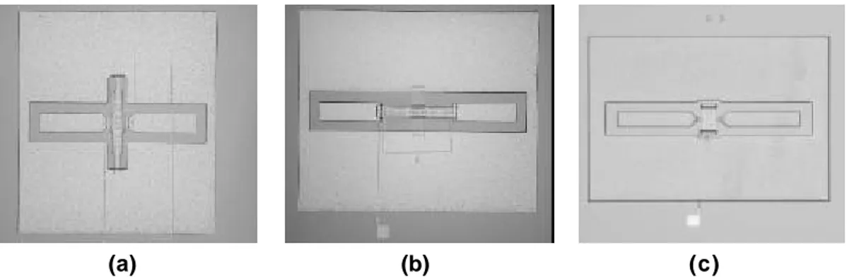
In the parallel (shunt) version of the SPST, which we call “classic” type, a metal membrane (movable air bridge) above the CPW substrate can electrically short the centre line to ground when electrostatically actuated, as shown in Figure 1(a). To avoid stiction problems a dielectric layer is placed between the centre line and the bridge.
Another type of the shunt SPST is the “longitudinal” type, shown in Figure 1(b). Here the bridge is part of the centre conductor; it is above an underpass metal strip, which connects the two ground metals of CPW.
In the series version of the SPST the centre line is interrupted and the gap can be closed by means of an electro-statically actuated metal membrane above it, as shown in Figure 1(c). In all switch types the resistors for the command signal and the capacitors for the DC isolation between command and RF signals are also built into the silicon device.
(a) (b) (c)
Figure 1 – Shunt version (classic type) of SPST (a); shunt version (longitudinal type) of SPST (b); series version of SPST (c).
To have an SPDT switch, two SPST switches only are needed in principle, one for each arm. However, none of the above described switches can meet the technical requirements. In particular, RF isolation between input and output port in “off” condition is not respected, thus a combination of series and shunt switches is needed. The configuration that has been chosen for the switch under development presents the following features [3 ]:
- 1 series SPST and 1 shunt SPST for each input arm; this configuration is chosen to improve input to output isolation without seriously degrading insertion loss;
- a “T” line to connect each arm to the output port;
- biasing lines with distributed resistance for the actuation command;
- DC block capacitors in the signal line to avoid the DC actuation voltage to be present at the input and output ports and avoid additional reflections.
To characterize the mechanical behaviour of the air-bridges of the switch, the layout has been implemented including five bridges of different length that are actuated by the same actuation signal. The capacitance of the total structure assumes values from about 2 to 10 pF in the 0 -60 V range of the actuation voltage. The voltage applied to the switch causes increments of the capacitance at the rate of about 2 pF, corresponding to the successive actu ations of the movable bridges [3].
3. The designed test bench
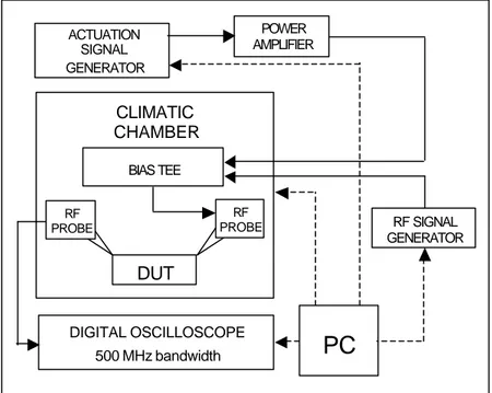
In order to characterize the performances of capacitive MEMS RF switches by means of parameters, such as actuation times, lifetime and RF signal attenuation, a test bench has been designed. The measurements are carried out by generating a RF waveform, by applying a periodic actuation signal to drive the switching events and by detecting the RF signal envelope at the output of the Device Under Test (DUT). As shown in Figure 2, the whole measurement system is managed by means of a computer.
The main actuation signal characteristics are: transition times of about 100 ns, duration of about 50 µs and frequency of 1 kHz. The power amplifier is used to achieve actuation voltages up to 40 V, thus making possible the actuation of the switch and long lifetimes [4]. Taking into consideration industrial applications for SPDT MEMS switches, a RF signal generator capable to generate sinewave signals up to 500 MHz has been chosen. Since the measured parameters depend only on RF signal envelope variations, an oscilloscope with a 500 MHz bandwidth can be used without affecting the measurement results.
In order to separate the RF waveform from the actuation signal, a bias tee is employed. As described in the following paragraph, an electrical network has been designed to obtain a bias tee matched to the DUT and the to oscilloscope. Finally, temperature and h umidity of the DUT environment is controlled by means of a climatic chamber.
Figure 2 – Block diagram of the measurement station.
4. The project of the bias tee
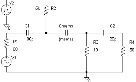
As figure 3 highlights, an electrical model of the test bench has been developed by using the PSpice tool. V1 and R1 represent the RF signal generator, V2 represents the actuation
voltage generator that determines the status of the switch, and R4 models the input
impedance of the oscilloscope. The behaviour of the capacitive MEMS RF switch has been modelled by a capacitor that assume discrete values of capacitance (Cmems). Taking as a
reference the data provided by preliminary measurements on the test structure , the value of Cmems has been evaluated between about 2 pF (switch open) and about 10 pF (switch close).
The resista nce R2, together with C1 and Cmems has been employed to realize two low pass
filters that strongly attenuate the RF components towards the pulse generator. Since the 3 dB bandwidth of V2 is of the order of 1 MHz, the values of R2 and C1 have been chosen to
obtain a minimum cut frequency of about 15 MHz. Similarly, Cmems (upper branch) together
with R3, C2 and R4 (lower branch) realize a high pass filter that rejects the actuation signal V2
at the oscilloscope input. For Cmems = 4pF, the rejection is higher than 100 dB at the
frequency of 5 MHz.
The attenuation introduced by the capacitive switch and its time domain response have been assessed by analyzing the envelope of the RF signal across R4, as a function of the Cmems
value. Switch attenuation is obtained as the ratio between the RF signal envelopes across R4
ACTUATION SIGNAL GENERATOR POWER AMPLIFIER CLIMATIC CHAMBER DUT BIAS TEE DIGITAL OSCILLOSCOPE 500 MHz bandwidth RF PROBE RF PROBE
PC
RF SIGNAL GENERATORfor Cmems = 2 pF and Cmems = 10 pF. The value achieved for V1=1 V is about 10 dB for
frequencies between 200 MHz and 1 GHz.
5. Conclusion
The project of a SPDT MEMS RF switch has been taken into account to design a test bench for testing time domain and reliability characteristics of capacitive MEMS RF switches. The specifics of the switch project that have been used to characterize the test bench include: values of the capacitance varying between 2 pF and 10 pF with steps of 2 pF and shape of the actuation signal depending on transition times of about 100 ns, duration of about 50 µs, frequency of 1 kHz and actuation vo ltages up to 40 V. On the basis of other parameters such as the maximum RF signal frequency of 500 MHz, the oscilloscope bandwidth of 500 MHz and electrical models of the measurement instrumentation, a bias tee has been designed in order to separate the RF waveform from the actuation signal. The obtained bias tee is composed of two low pass filters that cut the RF components above about 15 MHz at the input of the impulse generator and one high pass filter that attenuate of about 100 dB the actuation signal at the input of the oscilloscope. Application of the proposed test bench are in progress for measurements on advanced prototypes of the SPDT switch.
Bibliography
[1] Z. Yao, S. Chen, S. Eshelman, D.Denniston, and C. Goldsmith, Micromachined
low-loss microwave switches, Journal of Microelectromechanical Systems, Vol. 8, No. 4,
1999, p.129.
[2] J. Rizk, G-L Tan, J. Muldavin, G. Rebeiz, High-isolation W-band MEMS switches, IEEE Microwave and Wireless Components Letters, Vol. 11, No. 1, 2001, p.10. [3] C. Armaroli, L.. Ferrario, F. Giacomozzi, L.. Lorenzelli, B. T. Margesin, K. Rangra, G.
Tommaso, A silicon based MEMS technology for electro-statically actuated SPDT RF
switches, European Space Component Conference ( ESCCON), 2002
[4] C. Goldsmith, J. Ehmke, A.. Malczewski, B. Pillans, S. Eshelman, Z. Yao, J. Brank, M. Eberly, Lifetime characterization of capacitive RF MEMS switches, Proc. IEEE MMT-S International Microwave MMT-Symposium Digest, Vol. 1, 2001, p.227.