Università degli Studi di Catania
International PhD in Chemical Sciences
XXVI Cycle
Graphene and Related Materials: from
“Scotch-Tape” to Advanced Production
Methods
Paola Russo
Supervisor:
Chiar.mo Prof. G. Compagnini Coordinator:
Chiar.mo Prof. R. Purrello
PhD Thesis A.Y. 2010-2013
Index
Index ... i
Introduction ... 1
Chapter 1. Carbon Materials ... 6
1.1. Carbon in Nature ... 6
1.2. Carbon Compounds ... 7
1.3. Carbon allotropes in 3D: Graphite and Diamond .... 10
1.4. Carbon Allotropes in 0D: Fullerenes and Graphene Quantum Dots ... 13
1.5. Carbon Allotropes in 1D: Carbon Nanotubes and Polyynes (Carbynes) ... 18
1.6. Carbon allotropes in 2D: Graphene and Graphene-based materials. ... 30
1.7. Hybrid Nanomaterials: Definition ... 33
1.8. Carbon-based Hybrid Nanomaterials ... 36
1.8.1. Fullerene@SWNTs ... 37
1.8.2. Polyynes@CWNTs ... 41
1.8.3. Polyynes@Graphene ... 46
2.1. What is Graphene ... 49
2.2. Crystal Structure and Properties of Graphene ... 51
2.3. Overview of the potential applications of graphene . 57 2.4. Graphene synthesis ... 59
2.4.1. Mechanical Exfoliation ... 60
2.4.2. Chemical Exfoliation ... 62
2.4.3. Laser exfoliation of graphite ... 65
2.4.4. Chemical synthesis: Graphene from reduction of Graphene Oxide ... 73
2.5. Characterization techniques of graphene ... 75
2.5.1. Optical Microscope ... 76
2.5.2. Scanning Electron Microscopy (SEM) and Transmission Electron Microscopy (TEM) ... 78
2.5.3. Atomic Force Microscopy (AFM) ... 80
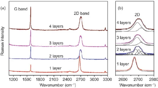
2.5.4. Raman Spectroscopy ... 82
2.6. Experimental results: mechanical and laser exfoliation ... 85
2.6.1. Mechanical exfoliation ... 85
2.6.2. Laser exfoliation of graphite ... 94
2.6.3. Mechanical versus laser exfoliation ... 101
3.1. Bottom-up and Top-down Approaches ... 103
3.2. Graphene Nanowalls (GNWs) ... 105
3.3. Bottom-up approaches for GNWs production ... 106
3.4. Characterization of GNWs ... 113
3.5. Applications of Graphene Nanowalls ... 115
3.6. Novel approach: Electric Field-Assisted Laser Ablation of Carbon in Water ... 116
3.7. Experimental results ... 120
3.7.1 GNWs growth: transport and growth mechanism of polyynes ... 126
3.7.2 Growth of the GNWs on different substrates. ... 130
3.8. Porous Graphene (PG) ... 131
3.9. Properties of PG ... 133
3.10. Potential Applications of PG ... 138
3.11. Synthesis of PG... 143
3.11.1 Modification of Suspended Graphene Sheets by Exposure to an Electron Beam ... 143
3.11.2 Graphene Sheets Etched with Nitrogen in a Scanning Electron Microscope (SEM) ... 145
3.11.3 Etching of Graphene Sheets by MnO2 ... 146
3.11.4 Photoreaction of Graphene Oxide in O2 under UV Irradiation ... 148
3.11.5 Novel Method for the Production of PG ... 150
3.12. Graphene Quantum Dots (GQDs) ... 151
3.13. Properties of GQDs ... 152
3.14. Applications of GQDs ... 156
3.15. Synthesis of GQDs ... 160
3.15.1 Hydrothermal and Solvothermal Method ... 161
3.15.2 Photo-Fenton Reaction of Graphene Oxide .. 164
3.15.3 Precursor Pyrolysis ... 166
3.15.4 Novel Method for the Synthesis of GQDs ... 168
3.16. Experimental results: Femtosecond Laser for the Synthesis of PG and GQDs ... 168
3.16.1 Formation of porous graphene (PG). ... 169
3.16.2 Formation of Graphene Quantum Dots. ... 176
3.16.3 Mechanisms proposed for the production of PG and GQDs. ... 180
3.16.4 Experiments in liquid nitrogen (N2). ... 186
Conclusions ... 193
Bibliography ... 195
List of Publications ... 237
Introduction
Nanotechnology is the act of purposefully manipulating matter at the atomic scale, otherwise known as the “nanoscale.”
The name “nanotechnology” derives from the Greek words
nanos, which means dwarf, and technologia, which means
systematic treatment of an art. The term was coined in 1976, when Norio Taniguchi outlined his vision of atom-by-atom or molecule-by-molecule manipulation of matter for the semiconductor industry.
Nowadays nanotechnology is used to describe the creation and exploitation of materials with structural features in between those of atoms and bulk materials, with at least one dimension in the nanometer. The science and technology of nanomaterials have created great excitement and expectations in the last few years. By its very nature, the subject is of immense academic interest, having to deal with very tiny objects in the nanometer regime. There has been explosive growth of nanoscience and technology in the last decade, primarily because of the availability of new methods of
synthesizing nanomaterials, as well as tools for characterization and manipulation. Furthermore, there is a better understanding of the size-dependent electrical, optical and magnetic properties of individual nanostructures of semiconductors, metals and other materials.
The top-down and bottom-up approaches are the terms used to classify nanotechnology, based on the technique used for the production of the nanostructures. Top-down methods consist of size reduction of larger structures, while the basis of bottom-up approaches is the employment of atomic or molecular precursors as building blocks materials for the construction of new nanostructures.
The properties of materials with nanometric dimensions are significantly different from those of atoms or bulk materials. Suitable control of the properties of nanometer-scale structures can lead to new science as well as new products. Most properties of solids depend on the microstructure, i.e. the chemical composition, the arrangement of the atoms (the atomic structure) and the dimensionality that is one of the most defining material parameters. The same chemical compound can exhibit dramatically different properties depending on whether it is arranged in a zero-dimensional
(0D), one-dimensional (1D), two-dimensional (2D), or three-dimensional (3D) crystal structure. In other words, if one changes one or several of these parameters, the properties of a solid will vary.
In recent years, many nanomaterials with different size, shape and structure have been discovered; these materials can show a metallic behaviour, or be semi-conductive or insulators, resulting in advanced applications in various fields. For example carbon-based nanomaterials play an increasingly pervasive role in nanoscale science, thus because the variety of crystallographic forms of carbon places this element into the focus of attention both in terms of basic research as well as applications.
My research project, during my PhD in Chemical Sciences, was the synthesis and characterization of carbon-based nanomaterials. In particular, during the first year of my PhD, I focused my attention on the synthesis of graphene, a carbon-based nanomaterial arranged in a two-dimensional (2D) crystal structure. The main purpose of the study was to optimize the method of synthesis of graphene, using the “Scotch-tape” technique, to obtain greater amounts of graphene compared to samples consisting of several layers. Although this technique
leads to high quality graphene sheets, it is not the suitable approach to obtain a gram-scale production of graphene for its employment in nanoelectronics.
During the second year, my studies focused on the synthesis and characterization of graphene-based nanomaterials. In particular, I have dealt with graphene nanowalls (GNWs), which consist of few graphene layers vertically oriented on a suitable substrate. These materials have attracted the interest of many researchers due to their potential applications as cathode materials for field emission devices.
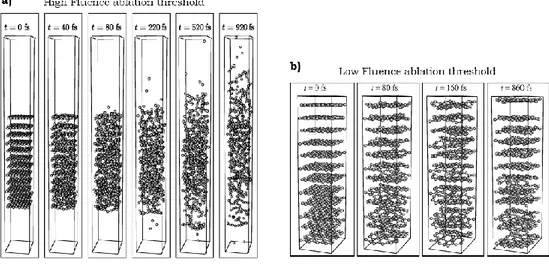
During the third and last year of my PhD, I studied the effects of ablation of a graphite target either with a nanosecond or a femtosecond laser, in liquids. In particular, I carried out my studies and experiments at the University of Catania and at the University of Waterloo (Canada) at the Department of Mechanical and Mechatronics Engineering, in the Centre for Advanced Materials Joining (CAMJ). It was found that the laser ablation of graphite can lead to the synthesis of large graphene domains employing the nanosecond laser, while the use of a femtosecond laser produces large amounts of porous graphene sheets, that are recovered at the water-air interface and the graphene quantum dots that are dispersed in the
liquid. These materials, the porous graphene and graphene quantum dots, are attracting the interest of all the scientific community due to their potential applications in many fields such as energy storage and water treatment, respectively. The main purpose of my whole research across these years was the study of new methods for the synthesis of graphene-based nanomaterials in order to employ them in nanoelectronics and environmental-oriented fields.
Chapter 1. Carbon Materials
1.1. Carbon in Nature
Carbon (from the Latin language, Carbo, which means coal) as a non-metal element is the 15th most abundant element in the Earth's crust and the fourth most abundant element in the universe by mass after hydrogen, helium, and oxygen. The extraordinary ability of this chemical element to combine with itself and other chemical elements in different ways is the basis of organic chemistry and of life, since it is part of DNA, proteins and so on. It is precisely this chemical versatility, which allows having a vast amount of carbon-based structures. The element is found free in nature and itself is used as coke in steel making to reduce iron oxide to iron, as carbon black in printing, and as charcoal in sugar refining. Carbon is also important environmentally as carbon dioxide; it is about 350 parts per million of the atmosphere, plants take it in as they grow and it is dissolved in all natural waters. Carbon is a component of rocks as carbonates of calcium (limestone), magnesium, and iron. It is also found in
abundance in the sun, stars, comets, and atmospheres of most planets.
1.2. Carbon Compounds
The carbon element is the first element of column IV, in the periodic table, and its ground state electronic configuration is [(ls2) (2s22p2)]. Out of its six electrons, four electrons in its
valence shell form three hybridizations (sp, sp2, sp3) which
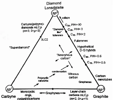
lead to the formation of many stable carbon structures, allotropes, in all dimensions. The classification scheme of carbon allotropes based on the concept of the hybridization type of the valence orbitals of the carbon atoms and the relationship of different hybridized carbon allotropes is shown in Figure 1-1. Carbon, is capable to be very hard or very soft, it has the highest melting point among all the known elements. The use of this unique chemical element is almost unlimited from the hardest diamond for drilling to the softest form, graphite, for using it as a lubricant and in skin health and beauty. The three-dimensional forms of carbon, diamond and graphite, are widely known. However, in the last decades many exciting carbon nanomaterials have been discovered, and
intensively studied due to their unique structure, electronic, mechanical, optical, and chemical characteristics.
Figure 1-1: Classification of the carbon allotropes based on the type of hybridization and relationship between them. [Taken from ref. (1)]
The property of a bulk material is largely determined by the types of the constituent chemical elements and the nature of the chemical bonds that ‘hold’ the atoms and molecules together to form the material. However, this ‘conventional wisdom’ no longer holds in the nanometer regime in which, in addition to the chemical bonds, the size, dimensionality, and shape also play important roles in determining the properties
of the materials, especially the electronic, magnetic, and optical properties. The size matters when it becomes comparable to the length scale of a certain physical phenomenon that is concerned. Depending on their relative sizes in different spatial directions, carbon compounds can be divided into categories of different dimensionality ranging from 3D to 2D, 1D and 0D. The above classification is introduced for materials with simple shapes such as slabs/sheets (2D), wires/tubes/rods (1D), and cubes/spheres (0D).
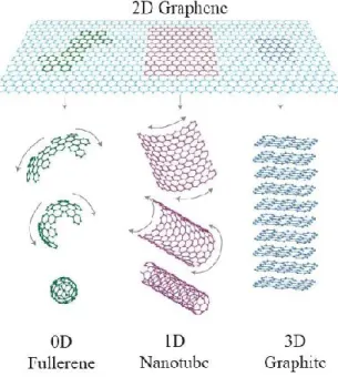
The most known allotropes of carbon, as mentioned before are diamond and graphite, then to these must be added the other crystalline forms, that have different dimensionality from the 3D. These allotropes are the fullerenes and the graphene quantum dots (0D), the carbon nanotubes and the polyynes (1D), and graphene and the graphene-based materials (2D). The structures and chemical bonding of all these crystalline forms of carbon are reviewed in the next paragraphs. In the paragraph 1.7, the carbon-based hybrid nanomaterials will be discussed, where with the term “hybrid nanomaterials” we refer to a class of materials that are unique conjugates of two different structures and have found applications and appeals in many fields.
1.3. Carbon allotropes in 3D: Graphite and
Diamond
Graphite and diamond are two different crystalline forms of the same element, and they exhibit different physical and chemical properties. If graphite can be is easily exfoliated, it is black, highly reflective and it behaves like a semimetal, the diamond on the contrary, is extremely hard, transparent and acts as an insulator. The main reason of these differences is related to the different crystal structure of the two allotropes. Graphite has a hexagonal crystal structure, and the basis of this crystal structure is the graphene plane, which is an extended hexagonal array of carbon atoms with sp2
-hybridazation. Graphite has two types of crystal forms: the hexagonal form and the rhombohedral one. The commonest and more stable form is the hexagonal, known also as alpha, where the stacking order of the layers is ABABAB..., shown in Figure 1-2. The rhombohedral form (or beta) with a stacking sequence ABCABC… is a minor component of well-crystallized graphite. The proportion of the beta form of graphite could be increased or decreased by deformation processes and by high temperature treatment, respectively (1). For both these crystal
forms of graphite the in plane C-C distance is 0.142 nm, an intermediate value between Csp3- Csp3 and Csp2=Csp2 bond
lengths, 0.153 and 0.132 nm, respectively. Each C-C bond in the carbon layer plane has about one-third double bond character.
Figure 1-2: Crystal structure of the hexagonal graphite
The distance between two consecutive layers in graphite, interlayer distance, is 0.335 nm that results from a different type of bonding. It is well known that within the planes, the carbon atoms arranged in the hexagonal lattice are covalently bonded, while there is no unanimity regarding the nature of the interlayer bonding. The common assumption has been that the interlayer forces are of the van der Waals type, even if other authors define it cautiously as “a much weaker force
than the in-plane covalent bond”. This could explain the easy exfoliation of graphite and its lubrication properties.
In diamond, the carbon atoms are arranged in a variation of the face-centred cubic crystal structure called a diamond lattice. Frequently diamond is found in a cubic form in which each carbon atom is linked to four other carbon atoms by sp3 σ
bonds in a strain-free tetrahedral array, as shown in Figure 1-3.
Figure 1-3: Crystal structure of diamond
The crystal structure is zincblende type and the C-C bond length is 0.154 nm. Diamond also exists in a hexagonal form (Lonsdaleite) with a Wurtzite crystal structure and a C-C bond length of 0.152 nm. Diamond is less stable than graphite, but the conversion rate from diamond to graphite is negligible at
ambient conditions. Most natural diamonds form at high-pressure and high-temperature conditions existing at depths of 140 to 190 kilometers in the Earth mantle.
Diamonds have been adapted for many uses because of the material's exceptional physical characteristics. Most notable are its extreme hardness and thermal conductivity (900– 2,320 W·m−1·K−1), as well as wide bandgap and high optical
dispersion. Above 1,700 °C in vacuum or oxygen-free atmosphere, diamond converts to graphite; in air, transformation starts at ~700 °C. In diamonds, the bonds form an inflexible three-dimensional lattice, whereas in graphite, the atoms are tightly bonded into sheets, which can slide easily over one another, making the overall structure weaker.
1.4. Carbon Allotropes in 0D: Fullerenes and
Graphene Quantum Dots
H. Kroto and R. Smalley (2) discovered fullerenes, C60
molecules, in the mass spectrum of laser-ablated graphite in 1985. The experiments that led to the discovery of the fullerenes aimed at understanding the mechanism by which long-chain carbon molecules formed in interstellar space and circumstellar shells. It was only in 1990 (3) that crystals of C60
molecules were isolated from soot formed from graphite arc electrodes. The C60 structure is also known as
Buckminsterfullerene, because of its resemblance to the geodetic domes built by R. Buckminster Fuller.
Figure 1-4: a) Crystal structure of C60; b) geodetic dome built by R.
Buckminster Fuller
The C60 molecule shows a regular truncated icosahedron
structure consisting of 20 hexagons and 12 pentagons. The 60 carbon atoms in C60 are located at vertices of the truncated
icosahedron and every carbon site is equivalent to every other site. The distance between the C-atoms and the centre of the molecule is about 3.55 Å, while the C-C bond length is 1.44 Å that is almost identical to that in graphite 1.42 Å. In the
fullerene, each carbon atom is trigonally bonded to three nearest-neighbour carbon atoms and it can be regarded as derived from the wrapping of a graphene sheet (single layer of crystalline graphite).
Beside the C60 structure, during its synthesis it is possible to
form larger molecular weight fullerenes Cn (n>60). The most
abundant is the C70 even if sufficient quantities of C76, C78 and
C84 are found. The crystal structures of these molecules are
more complex than that of the C60 molecules. The C70 molecule
shows an ellipsoidal crystal structure, presents D5h symmetry,
and contains 37 faces (25 hexagons and 12 pentagons) with a carbon atom at the vertices of each polygon and a bond along each polygon edge, Figure 1-5. Its structure is similar to that of C60 molecule but has a belt of six hexagons inserted at the
equator. The molecule has eight bond lengths ranging between 1.37 and 1.46 Å. Each carbon atom in the structure is bonded covalently with three others (4). At high temperature (T >> 340 K), the fcc phase (a=15.01 Å) of C70 with freely rotating
molecules is most stable, but since the ideal hexagonal close packed (hcp) phase with c/a= 1.63 is almost equally stable, fcc crystals of C70 tend to be severely twinned and show many
a=b=10.11 Å and a larger c/a ratio of 1.82 occurs at about 340 K. The higher mass fullerenes (C76, C84), with multiple isomers
of different shapes, also crystallize in the fcc structure at room temperature, with an fcc lattice constant which is approximately proportional to n1/2, where n is the number of
carbon atoms in the fullerene (1).
Figure 1-5: Crystal structure of C70
In the past few years, another zero-dimensional form (OD) of carbon has attracted and continues to attract the interest of many research groups. In particular, we can indicate it as “the zero-dimensional form of graphene”, which are called “graphene quantum dots”. During the past years, these 0D
forms have been much less studied than graphene, carbon nanotubes and fullerenes, but recently, there has been significant advancement in both the theoretical and experimental fronts. The increasing interest towards graphene quantum dots (GQDs) is related to their unique optical and electronic properties due to their quantum confinement and edges effects.
Figure 1-6: Applications of graphene quantum dots [Taken from ref. (5)]
Their properties differ from those of 2-D graphene and have great potential for a variety of applications principally in photovoltaic devices (6) and bio-related applications such as fluorescence labelling and bio-imaging (7). The common way to
describe the graphene quantum dots is referring to them as graphene sheets (less than 10 layers in thickness) whose dimensions are in the range from few nm to ~100 nm, as quantum confinement effect has been clearly observed in graphene dot of 110 nm in diameter (8).
1.5. Carbon Allotropes in 1D: Carbon Nanotubes
and Polyynes (Carbynes)
In 1991, during the study of the surface of some carbon electrodes used in the manufacture of fullerenes (9) in an arc discharge tube, Iijima noticed the presence of structures consisting of several concentric tubes of carbon; the so-called “carbon nanotubes” were discovered. This new “nano-allotrope” of carbon consists of two separate regions with different physical and chemical properties. The first is the sidewall of the tube and the second is the end cap of the tube, which presents a structure similar to fullerene C60 (10). The
structure of carbon nanotubes (CNTs) can be thought deriving from the cylindrical folding up of graphene sheets (honeycomb lattice of carbon atoms) with a wide range of diameters between 1 and over 80 nm (depending on the number of walls comprising the nanotubes) and with a length that exceeds 10
µm. The length to diameter ratio is about 1000 for most of the CNTs, so they are considered as one-dimensional structures (1D). Therefore, these materials are expected to possess additional interesting electronic, mechanical and molecular properties.
Figure 1-7: Structure of a carbon nanotube
Carbon nanotubes are distinguished depending on the number of graphene sheets comprising the nanotubes. In particular, carbon nanotubes composed of one graphene sheet are labelled as single-wall carbon nanotube (SWCNTs or SWNTs), those made of two graphene sheets as double-wall carbon nanotubes (DWCNTs or DWNTs), while the multi-wall carbon nanotubes (MWCNTs or MWNTs) are composed of many graphene sheets.
Figure 1-8: Structure of: a) SWCNTs, b) MWCNTs
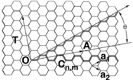
One of the most interesting features of carbon nanotubes is that they could exhibit either metallic or semiconducting behaviour depending only on diameter and helicity of the arrangement of graphitic rings in their walls (11; 12).The graphene sheets can be rolled up in different ways, which lead to various helical structures. Precisely, the vector connecting two crystallographically equivalent lattice points (the points O and A in the Figure 1-9) in an unrolled honeycomb lattice, i.e. the graphene sheet, defines the structure of a carbon nanotube. When the two points coincide (aim achieved by the rolling up of the graphene sheet), a tube with a circumference corresponding to the line AO is produced. The vector connecting the two lattice points, A and O, in an unrolled graphene sheet is called the chiral vector, and it is
perpendicular to the tube axis. The chiral vector can be expressed with two fundamental translational vectors a1, a2:
Where n and m are integers with 0 ≤│m│≤ n, and a1, a2 are the
primitive unit cell vectors in the basal plane of the graphite structure.
Figure 1-9: SWCNT geometry. Lattice vectors are denoted a1 and a2, while the
OA vector is the Ch chiral vector. The θ angle is the chiral angle of the
nanotube. [Taken from ref. (13)]
The structure of SWNTs is specified by the set of two integers (n, m) labelled as chiral indices. The diameter dt and the chiral
angle θ, depicted in Figure 1-9, can be expressed in terms of n and m
Where (14).
Depending on the chiral indices, the carbon nanotubes are distinguished in:
Armchair type, when
Zig-zag type, when
Chiral type, when
Figure 1-10: Different chirality of SWNTs
The diameter of the SWNTs depends on the synthesis conditions and especially on the diameter of the catalyst particles employed for the synthesis (14), and it ranges from 0.7 to 3 nm. The MWNTs, as mentioned before, consist of many graphene sheets (from 2 to about 40) rolled up, their diameters are in the range of 4-50 nm and their lengths are around 10 µm. The interlayer distance between the rolled graphene sheets is 0.344 nm that is 2.5% wider than the value presented by the graphite (0.3354 nm).
For what concern the electrical properties of the CNTs, the electronic band structure calculations predict that the (n, m) indices determine the metallic or semiconducting behaviour of SWNTs. When n - m = 3j, where j is an integer, the tube is
metallic, otherwise when n - m ≠ 3j the tubes are semiconductors.
Figure 1-11: Electrical behaviour of SWNTs
The energy gap of semiconducting carbon nanotubes is inversely proportional to the diameter of the tube, and to be independent of the chiral angle θ. According to the tight bending calculation, the equation for the energy gap Eg is:
Where is the nearest neighbour interaction energy, = 0.142 nm being the carbon-carbon bond distance, and is the nanotube diameter (15).
For what concern the electric properties, the carbon nanotubes exhibit quantum mechanical electric transport phenomena owing to their small size and structural perfection. The metallic CNTs can act as wires, while the semiconducting ones can be seen to act as transistors (14).
For their high stiffness, coupled with their low density, nanotubes might be useful as nanoscale mechanical parts. It is predict by theoretical estimates, that the carbon nanotubes possess a Young’s modulus of the order of 1 TPa. Moreover, carbon nanotubes retain unusual strength in the large-strain region. The CNTs can be bent up to 110º without undergoing catastrophic fracture being extraordinarily flexible and resistant (14).
As mentioned in the previous paragraphs, due to the strong carbon-carbon chemical bonds and to the light mass of carbon atoms, carbon materials such as graphite and diamond show the highest thermal conductivity among materials. Phonons (lattice vibrations) are the major and exclusive carriers of heat for graphite and diamond, respectively. Since, the thermal
conductivity of a material strongly depends on the grain sizes in the sample, CNTs exhibit a thermal conductivity equal or higher than those of graphite parallel to the basal planes (~3000 W (m∙K)-1 at 100 K) and natural diamond (~104 W
(m∙K)-1 at 80 K), due to their high crystallinity and
directionality (14).
The other one-dimensional carbon allotropes are the carbynes, which are linear chains of carbon atoms. In particular, carbyne is supposed to occur in two isomeric forms: the polyynes and the polycumulene. The carbon atoms in the polyynes present conjugated C(sp1)≡C(sp1) bonds, while the
polycumulenes possess cumulated C(sp2)≡C(sp2) double
bonds.
El Goresy and Donnay (16) first discovered polyynes in 1968; in their work, they call this new form of carbon as “white carbon” or Chaoite, which presents a hexagonal crystal structure. At the same time, other two groups published a series of papers reporting the discovery of other carbyne forms with hexagonal structures named as Carbon-VI, VII, IX etc. formed in experiments involving attempts to vaporize graphite at 2550 K and low pressure (17; 18), and by
dehydropolymerisation of acetylene: α-carbyne and β-carbyne (19; 20).
Table 1.
Crystal structure data for some carbynesCarbyne Chaoite α-carbyne β-carbyne Carbon VI
Structurea hex hex hex rhomb.
a0/pm 895 894 824 923
c0/pm 1408 1536 768 1224
Densityb 3.43 2.68 3.13
Ref. (16) (19) (20) (19) (20) (17) (18)
a-hex= hexagonal, rhomb.= rhombohedral; b= g∙cm-3
Table 1: Lattice parameters for some of these carbyne forms [Adapted from ref. (1)]
Despite many publications on carbynes, the acceptance of the existence and significance of polyynes is still a slow process. This skepticism is related to the fact that polyynes are unstable; they have a strong tendency to be oxidized by the oxygen that causes their destruction (21; 22; 23). Moreover, because the carbyne structure requires stabilization, these linear carbon chains lean to undergo chain-chain cross-linking reaction towards sp2 graphene structures as a final product
(21), avoiding the possibility to isolate carbynes as large crystal forms.
Figure 1-12: Chain-chain cross-linking reaction of polyynes [Adapted from ref. (21)]
Polyynes have been studied in the gas phase and they have been found in the interstellar molecular clouds (24; 25). Different routes can artificially produce these linear carbon chains. Some are listed below: the oxidative dehydropolycondensation of acetylene, the polycondensation of carbon sub-oxide with bis(bromomagnesium) acetylide, reactions based on the chemical transformations of polymers (dehydroalogenation of halogen-containing polymers, defluorination of polytetrafluoroethylene, dehydrogenation of polyacetylene, condensation of carbon vapour produced by various techniques, e.g., laser ablation of graphite and arc discharge (26).
During the last years, a series of papers were published regarding the possibility for the creation of new materials based on carbynes. First all, carbynes are semiconducting materials and this feature opens up prospects for creation of a new element basis for microelectronics based on carbon only. Secondly, carbyne is a high-temperature phase of carbon, which is stable at T>2000ºC. It is distinguished from other carbon materials by its stability with respect to the formation of compounds with hydrogen; this makes polyynes very promising for application as the material of the first wall in devices for controlled thermonuclear fusion. Moreover, it is found that carbyne has a potential application in medicine due to its high biocompatibility and no toxicity. In particular, carbyne-containing polymers materials could be employed in reconstructive surgery, thus because they can be implanted into living organisms and be in contact with native blood for a long time. These materials are available as fibers, films or the coating bearing the carbyne surface layer, which serves as a protective coating (26).
1.6. Carbon allotropes in 2D: Graphene and
Graphene-based materials.
In the last 30 years, there have been numerous reports studying the 0D, 1D and 3D materials, although it is in the 2D systems that the top-down and bottom-up approaches of the nanotechnology are currently being developed. Noteworthy, research works based on the synthesis of 2D materials, as isolated forms, are dated from the past ten years.
More than 70 years ago, Landau and Peierls argued that strictly two-dimensional (2D) crystals were thermodynamically unstable and are not possible to exist. Their theory pointed out that a divergent contribution of thermal fluctuations in low-dimensional crystal lattices should lead to such displacements of atoms as they become comparable to interatomic distances at any finite temperature. The argument was later extended by Mermin and has been strongly supported by many experimental observations. Indeed, the melting temperature of thin films rapidly decreases with decreasing the thickness, and they become unstable (segregate into islands or decompose) at a thickness of, typically, dozens of atomic layers. For this reason, atomic monolayers have so far been known only as an
integral part of larger 3D structures, commonly grown epitaxially on top of monocrystals with matching crystal lattices.
Graphite, as described previously, is a layered material with strong in-plane bonds, however the van der Waals-like couplings between the layers weaken the structure. Because of this layered structure, many researchers tried to split such materials into individual atomic layers, although it remained unclear whether freestanding atomic layers could exist in principle. This common knowledge was contradicted in 2004 by the experimental discovery of graphene by Geim and Novoselov (27) and other freestanding 2D atomic crystals such as the graphene nanowalls (28; 29) and the single layers of boron nitride (30).
The most intriguing material, among the aforementioned 2D forms of carbon, is graphene (Chapter 2). It is a monolayer of sp2-bonded carbon atoms arranged in a honey carbon lattice.
Since its discovery in 2004 (27), it has revolutionized all the scientific field due to its exceptional electrical, physical and chemical properties and its discoverers (Geim and Novoselov) earned the Nobel Prize in Physics in 2010. The promising
applications of this exceptional material have opened up new opportunities for future devices and systems.
It was reported, that modifying the structure of graphene (basal planes or edges) it is possible to improve the graphene properties, so the interest towards the fabrication of new graphene-based materials is growing among many research groups. These new types of materials can be employed for the design of nanoscale transistors (31), gas sensors (27), fuel cells (32), solar cells (33), organic light-emitting diodes (OLEDs) displays (34), and bio-related sensors (7). Many works are focusing on the synthesis of graphene nanowalls (GNWs), which are two-dimensional carbon nanostructures standing vertically on a substrate and they are considered one of the most promising graphene-based materials used in nanoelectronics as field emitters (35), (36). Recently, is growing the scientific interest towards other graphene-based materials such as porous graphene (PG) and graphene quantum dots (GQDs). The former is described as a graphene sheet with some carbon atoms vacancies (holes/pores) in the plane, while the latter are zero-dimensional materials and can be regarded as small fragments of graphene sheets with dimensions less than 100 nm. Both these materials are attracting the interest
of many researchers for their unique properties. For instance, porous graphene for its particular spongy structure has been suggested as a suitable membrane for gas separation (37), energy storage (38; 39), and as a basic material in nanoelectronics applications (40; 41). Otherwise, graphene quantum dots have potential applications in photovoltaics, water treatment (42) and in bio-related applications (7). These graphene-based materials will be discussed in depth in the next chapters.
1.7. Hybrid Nanomaterials: Definition
Products and their properties have to meet increasingly high and complex requirements. They are expected to offer a wide range of functions, weight as little as possible, be easy to handle and cost little to buy and maintain. This cannot always be achieved to the desired extent using classic materials. Scientists and engineers realized on, that mixtures of materials can show superior properties compared with their pure counterparts. It was only at the end of the 20th and the beginning of the 21st century that it was recognized by scientists, due to the availability of novel physical–chemical characterization methods, that the field of nanoscience could
open many perspectives for approaches to new materials. The combination of different analytical techniques gives rise to novel insights into hybrid nanomaterials and makes it clear that bottom-up strategies from the molecular level towards materials’ design will lead to novel properties in this new class of materials.
If we have to give an answer to the common question: “what is a hybrid nanomaterial?” we can state that hybrid nanomaterials are unique conjugates of two different structures. In particular, the term hybrid in a simplistic manner, as reported by Bhanu P. Chauhan (43), means fusion, union, or combination of the features, into one monolithic identity to exploit the advantages of combined features and to negate the disadvantages of the individual components. Makisima (44) defined hybrid materials as mixtures of two or more materials with newly formed chemical bonds. The categorization of hybrid materials and their related materials was proposed as follows:
1. Composites: Mixture of materials consisting of matrix and micron-level dispersion
2. Nano composites: Sub-micron level mixture of similar kinds of materials
3. Hybrids: Sub-micron level mixture of different kinds of materials
4. Nano-hybrids: Atomic or molecular level mixture of different materials with chemical-bonds between their different materials
Makisima explained that the difference between hybrids and nano-hybrids was not so obvious, and that nanocomposites include hybrids and nano-hybrids in many cases. On the other hand, Ashby (45) defined hybrid materials as "a combination of two or more materials in a predetermined geometry and scale, optimally serving a specific engineering purpose". Hagiwara and Suzuki (46) described hybrid materials as an intentional combination of two or more materials, complimenting each other to have super-functions or new functions, which component materials did not possess. According to their criterion, the difference between hybrid materials and composites lies in their functions and/or properties, specifically hybrid materials are presumed to show superior functions or properties comparing to traditional composites. Although there is no a single definition for these materials, unique is the idea that drives many researchers to the synthesis of these hybrid materials, namely the creation of this
new class of materials leads to fusion of the desired properties with the elimination of undesired behaviour providing an appealing property profile for such materials. For this reason, these materials have many potential applications in various fields even though their original components might not have been considered for those applications (43).
1.8. Carbon-based Hybrid Nanomaterials
Physical properties of carbon based nanomaterials (i.e., fullerenes, carbon nanotubes, polyynes and graphene) are an attractive platform for applications in optoelectronics and photovoltaics. They can act as semiconductors, metals, and dielectrics. Moreover, these materials can be transparent or opaque, and their surfaces may be passive (basal planes of graphite) or chemically active (edge planes of graphite). Thus, numerous variations of mechanical, electrical, or chemical properties can be achieved by using carbon nanomaterials and controlling their structure and surface chemistry, i.e. the band gap of semiconducting nanotubes or nanodiamonds can be tuned by changing the size and/or the doping elements.
As aforementioned, combinations of these carbon materials can create new carbon-based hybrid materials, enlarging the
area of their applications. For example, solar cells based on mixture of carbon nanotubes and carbon fullerenes (47) demonstrated enhanced efficiency, while SWCNTs filled with fullerenes (48; 49) have been realized and are expected to have a crucial influence in computing architectures.
In the next three sub-paragraphs, it will be briefly discussed about three carbon-based hybrid nanomaterials: the fullerene@SWNTs (Fullerene Peapods), the polyynes@SWNTs and the polyynes@graphene. The last two types of carbon hybrids materials have been synthesized by my research group and me and the results have been already published (50; 51).
1.8.1. Fullerene@SWNTs
The Fullerene@SWNTs, also known as fullerene peapods, where synthesized for the first time by Smith et al. in 1998 during the pulsed laser vaporization of graphite in presence of metallic catalysts (52). In this type of hybrid material, the fullerenes C60 are encapsulated inside the nanotubes, as
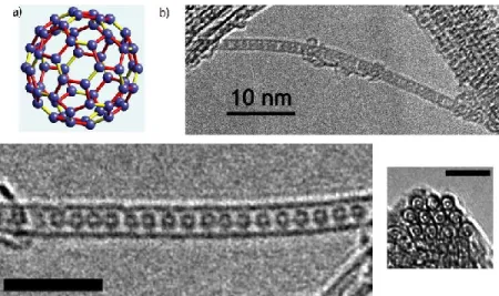
Figure 1-13: Fullerene@SWNTs. The figure shows the fullerenes molecules (a) trapped inside the nanotubes (b) [taken from
http://www.stanford.edu/group/GGG/1D.html]
The fullerene peapods can be classified according to the type of their two constituents, the host nanotubes and the encapsulated fullerenes. The classification is given according to the type of: a) the nanotube; b) the fullerene and c) the arrangement of the fullerenes inside the nanotube (53).
According to the type of nanotube, we can have:
1. Fullerene@SWNTs as synthesized by Smith in 1998 (52).
2. Fullerene@MWNTs synthesized the first time in 2003 (54; 55).
3. Non-carbon nanotubes such as the multi-wall boron nitride nanotube peapods, synthesized in 2003 (56).
According to the type of fullerene, the classification is: 1. Pristine fullerene (C60, C70) (52)
2. Endohedral fullerenes (referring to the icosahedral C60 symmetry (57)), that is, Endohedral
metallofullerenes (58; 59) and the N@C60 fullerene
(60)
3. Functionalized fullerenes (61) 4. Heterofullerenes (62; 63)
5. 13C isotope enriched fullerene peapods (64)
According to the arrangement type, the encapsulated fullerenes can form a linear chain (52) or can organize themselves in a ‘silo’ configuration (56) in larger diameter nanotubes. Since their discovery, fullerene@SWNTs, have been widely studied due to their anticipated unique electronic properties and potential applications, e.g., in high temperature superconductors (65).
Figure 1-14: "silo" arrangement of fullerene peapods inside CNTs [taken from ref. (53)].
This type of carbon hybrid could be employed also as transistors; they can alone act as solar cells as they have the active medium as well as the electrode naturally integrated. Indeed, solar cells consist of an active medium, which provides an electron-hole pair upon light excitation, which are separated from each other with an electrode. Li et al. (66) in their work, reported that fullerenes encapsulated inside SWCNTs act as the active electron-hole producing medium.
1.8.2. Polyynes@CWNTs
In the 1.5 paragraph, it was mentioned that, polyynes are very unstable and they can easily undergo to degradation. Due to their conjugate π electrons, that are doubly degenerated, they are expected to be better candidates for molecular devices than the carbon nanowires (CNWs) because polyynes are smaller than CNWs. Moreover, it was found by Zhao et al. that CNWs are much more stable inside the inner tube of MWCNTs (67).
Figure 1-15: Polyynes@SWNTS [Taken from ref. (68)]
For this reason, it is plausible to hypothesize the stabilization of polyynes inside SWNTs, where the walls protect the
polyynes avoiding their destruction. The hybrid materials that result from the combination of polyynes and the SWNTs are commonly indicated as “polyynes@SWNTs”. A schematic model is shown in Figure 1-15. The polyynes@SWNTs were synthesized by Nishide and co-workers incorporating chromatographically purified C10H2 into SWNTs by the
liquid-phase doping method (68). The evidence for the incorporation of the polyynes inside the SWNTs was provided by the Raman spectroscopy.
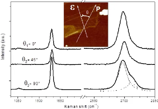
Raman spectroscopy is a powerful technique to study the vibrational properties of the carbon-based materials. In particular, it is very sensitive to the type of hybridization of the carbon atoms. The different carbon materials possess different Raman features that permit to distinguish them from each other. The sp-hybridized linear carbon chains, polyynes, generally show Raman bands around 1800-2100 cm-1, related
to the carbon triple bonds. The position of these bands varies with the length of the chain. In particular, it was predicted by Kastner (69) a shift of the bands to lower frequencies with increasing chain length. In the figure below are reported the Raman spectra, taken from ref. (68), of the pristine SWNTs (black line) and the one relative to the hybrid material made of
polyynes inside the SWNTs (red line). In particular, the signal at 2066 cm-1, is associated with the vibrational frequency of
sp-carbon bonds in the polyyne molecules and it is consistent with the presence of trapped polyynes inside SWNTs.
Figure 1-16: Raman spectra of pristine SWNTs (black line) and of polyynes@SWNTS hybrid material [Taken from ref. (68)].
In 2010 my research group and me, we were successfully able to synthesize polyynes inside multiwall carbon nanotubes (MWCNTs), also known as polyynes@MWNTs (50).
The hybrid materials were produced by arc discharge of two graphitic electrodes submerged in liquid nitrogen. During our experiments, we noticed that the experimental parameters influenced the structure properties of the materials produced. In particular, we found that the electrode size and the values of the discharge current play a key role on the quality of the nanotubes and on the type of nanotubes produced (CNTs and/or polyynes@MWNTs) (50). The analysis characterization of the systems obtained, such as Raman and TEM confirmed the presence of linear carbon chains trapped inside the MWNTs as shown in Figure 1-17. The presence of the peak at ~1850 cm-1, that is in the region of the sp-carbon bonds
vibrational frequency (1800-2200 cm-1) is consistent with the
presence of trapped polyynes inside the MWNTs. If we compare the Raman spectrum we obtained analyzing our samples with the one obtained by Nishide (68), we can noticed that the peak at 1850 cm-1 is red-shifted, thus because, as aforementioned,
theoretical studies suggest a red-shift of the sp Raman features with increasing chain length (69). Noteworthy, our results are consistent with the results reported by Zhao et al. (67), who first reported the presence of a carbon chain inside MWCNTs.
Figure 1-17: Raman spectrum of polyynes@MWNTs. [ref. (50)]
1.8.3. Polyynes@Graphene
Linear carbon chains, as mentioned in the previous paragraphs, are very unstable and they easily tend to undergo chain-chain cross-linking reactions towards more stable sp2
phase and for such a reason it is very difficult to obtain Raman spectra of isolated and well-identified polyynes. For this reason, polyynes are usually investigated by SERS (Surface Enhanced Raman Scattering) that permits to enhance the signals of the polyynes with the use of silver nanoparticles, thus because the resulting enhancement of Raman cross sections can be attributed to the excitation of the surface plasmon resonance in the silver nanoparticles (70).
Recently, many works proposed graphene as a suitable substrate for SERS, due to its electronic structure, which can promote charge transfer phenomena. In particular, graphene could amplify the Raman signal for probe molecules at high bond conjugation, disposed parallel to the graphene surface, as reported by Ling (71) and Naumenko (72).
In order to investigate the potential application of graphene as a SERS substrate, in 2011 my research group and me, we produced a new sp-sp2 hybrid carbon nanostructure composed
the solution containing the polyynes was drop casted on the top of the graphene layers, we observed a remarkable change of the graphene electronic and phononic behavior after the interaction with the linear carbon chains.
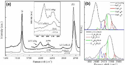
Figure 1-19: Experimental Raman spectra of LCCs deposited on single layer graphene (LCCs/SLG) compared with LCCs on silver nanoparticles (LCCs/Ag) and SLG spectra. Raman spectrum of LCC solution deposited on SiO2 is also shown for comparison. In the inset, a magnification of the 1700–2300 cm_1 region is shown. (b) Magnification of the 1800–2500 cm_1 region is shown for
LCCs/Ag and LCCs/SLG and compared with DFT calculations of the Raman active modes of single chains HAC2nAHinteracting with Ag and SLG units
[Taken from ref. (51)]
The SERS activity of graphene layers (SLG) towards the polyynes was examined in comparison with the other enhancer systems (silver colloids). If we look at the Raman spectra reported in Figure 1-19, we can see that the polyynes signals
without any enhancer system show only the signals relative to sp2 phase, due to their tendency to interchain crosslinking
when they are not stabilized. When polyynes were deposited on the top of a graphene layer, their signals were enhanced, thus confirming the possibility to use graphene as a SERS substrate (51).
Chapter 2. Graphene
2.1. What is Graphene
“Graphene”, is the name given to the carbon allotrope made of a planar monolayer of carbon atoms arranged into a two-dimensional (2D) honeycomb lattice.
Among the other carbon structures, graphene plays a very important role, as it is the basis for the understanding of the electronic properties in other allotropes, since it is considered as the building block of the other carbon allotropes. According to that common thought, fullerenes derive from the wrapping of graphene, while from its rolling up, the carbon nanotubes are obtained. The stacking of many graphene layers along the z-axis leads to the formation of graphite, as schematically showed in Figure 2-1. As mentioned in the previous chapter, graphene was studied theoretically for more than sixty years, and its existence was thought to be impossible, thus because it was believed that 2D materials did not exist without a 3D base. However, in 2004, the scientific world had to change his mind, when Geim and Novoselov demonstrated experimentally the existence of graphene (27). Such discovery has revolutionized the field of electronics owing to the excellent electronic and mechanical properties and chemical stability of graphene, which paves the way for many potential applications from nanoelectronics to the biochemical field.
2.2. Crystal
Structure
and
Properties
of
Graphene
Graphene is a single layer of carbon atoms packed into a two-dimensional hexagonal crystal lattice. The lattice of graphene consists of two equivalent interpenetrating triangular carbon sublattices A and B, each one contains a half of the carbon atoms. The primitive cell of graphene is composed of two non-equivalent atoms (Figure 2-2), indicated as A (black circles) and B (white circles), each forming a triangular 2D network, but translated from each other by a carbon-carbon distance equal to .
The lattice vectors can be written as:
,
where is the lattice constant.
The honeycomb structure is not a Bravais lattice because the atomic positions A and B are not equivalent, and for this reason, they cannot be connected with a lattice vector
, where n1 and n2 are integers. If we look only at
the A atomic positions (or the B atomic positions) they make up a hexagonal Bravais lattice and researchers usually refer to them as the A sublattice (or B sublattice).
The primitive reciprocal lattice vectors b1 and b2, satisfying
and are given by
,
The resulting reciprocal lattice is shown in Figure 2-3, which is a hexagonal Bravais lattice. The first Brillouin zone (BZ) is
hexagonal as shown in the figure below and it has a side length of 4π/3a.
Figure 2-3: First Brillouin zone of graphene [Adapted from ref. (74)]
The corners of the first Brillouin zone are called K or K’ points, which are also referred to as Dirac points, because the energy spectrum at these corners can be described by the mass less Dirac equation. Their positions in momentum space are given by:
,
Each carbon atom within a single plane has three nearest neighbors: the sites of one sub-lattice (A –black circles) are at
the centers of triangles defined by tree nearest neighbors of the other one (B – white circles). The positions of the three nearest-neighbor vectors in real space are given by:
, ,
The structure of graphene, composed of two equivalent triangular carbon sublattices, has important consequences for the electronic properties of graphene. The ground-state electronic shell configuration of carbon atoms is 1s22s22p2. It
has six electrons; four of them are valence electrons, while the other two are core electrons. In graphene, the carbon atoms have sp2 hybridization, generated by the superposition of 2s
orbitals with two of the 2p orbitals, the 2px and 2py orbitals
precisely. These orbitals lie in the graphene plane; they are oriented 120º to each other and form the energetically stable and localized σ-bonds with the three nearest-neighbor carbon atoms in the honeycomb lattice. The remaining free 2pz orbital
for each carbon atom lies perpendicular to the plane and presents π symmetry orientation. The overlap of these orbitals states between neighboring atoms plays an important role in the electronic properties of graphene.
The band structure obtained from the tight-binding model produces symmetric conduction and valence bands with respect to the Fermi energy, also called the charge neutrality
point or Dirac point, set at 0 eV. Since there is no band gap
between the conduction and valence bands graphene is usually designated a semimetal material with no overlap or zero-gap semiconductor (75).
Since graphene was discovered, its electronic properties have attracted the interest of the researchers, who looked at graphene as substitute of silicon in the fabrication of electronic devices. However, the absence of an energy band gap that restricts its use for digital applications, lead many researchers for searching alternative strategies capable of inducing a band gap in graphene sheets. For example, chemical doping, interaction with substrates and the application of external electric/magnetic fields are only some of the strategies that have been proposed so far. Besides the fascinating electronic properties of graphene, also its outstanding mechanical properties have attracted interest for electronic applications, since graphene holds great promise as a building block in nanoelectro-mechanical systems (NEMS), which are devices integrating electrical and mechanical
functionality on the nanoscale. The name derives from typical device dimensions in the nanometer range, leading to low mass, high mechanical resonance frequencies, potentially large quantum mechanical effects such as zero point motion, and a high surface-to-volume ratio useful for surface-based sensing mechanisms (76). The materials utilized for the fabrication of these devices have been the carbon-based materials; in particular, researchers employed carbon nanotubes and graphene, because the properties of these materials meet the needs of NEMS. In fact, the mechanical properties of graphene, such as the large Young’s modulus, are fundamental to the stability of NEMS, while its semiconductor activity allow graphene to function as transistors. Consequently, the study of the mechanical properties of graphene becomes crucial for the design and control of nanographene devices. The NEMS devices are functional only in response to an external applied force and it is beneficial to have the active element having as low mass as possible and as high of a quality factor as possible (77). The highest limit would be a one atom thick resonator and reaching this limit requires robustness, stiffness and stability of the material employed (78). Compared to silicon-based
materials, graphene is very strong and stiff and during these years, many researchers worked on the measurement of the Young’s modulus of graphene with both experimental and molecular dynamics (MD) simulation approaches. The Young’s modulus is a measure of the stiffness of a material, of graphene in this case, and together with the other two elastic parameters, the shear modulus and the Poisson’s ratio, defines the mechanical properties of graphene. The value of the Young’s modulus ranges from 0.5 TPa (79), measured using atomic force microscope (AFM), to 1.0 TPa calculated by Lee et al. (80), who measured the elastic properties and intrinsic breaking strength of free-standing monolayer graphene membranes by nanoindentation in an atomic force microscope, and their experiments established graphene as the strongest material ever measured.
2.3. Overview of the potential applications of
graphene
All these outstanding properties of graphene render it a unique material, for which a cornucopia of potential applications has been proposed so far. Many researchers showed that modifying the surface of graphene (basal planes or edges) it is possible to
modify the properties of graphene in order to employ it for the design of nanoscale transistors (31), gas sensors (27), fuel cells, energy storage and organic light-emitting diodes (OLEDs) displays (34). Recently, some studies showed that the graphene-based OLEDs can increase the performance of indium tin oxide (ITO) compounds, used in transparent conductive electrodes (81), and also graphene would be better in terms of being more flexible, less fragile, and having the potential of being cheaper than ITO. Graphene is able to withstand more strain than materials such as ITO while retaining its electrical properties (34). Bae and coworkers in their study reported that while an ITO touch-screen broke under 2-3% strain, a graphene touch-screen withstood up to approximately 6% and was limited by the electrodes on the screen rather than by the graphene itself (34). Graphene can also be used in the medical field for the design of nanosensors that can lead to detect illnesses (82).
The widespread research into the properties and applications of graphene attests to the growing interest in this fascinating material. Graphene’s strength and flexibility, together with its interesting charge carrier and other properties, can improve the existing technologies and can pay the way for the
development of new ones. In the next paragraphs, the different production techniques of graphene will be described.
2.4. Graphene synthesis
Since the discovery of graphene in 2004, several methods have been proposed for its synthesis. These methods consist of either top down approaches or bottom up ones. As a rule, the top-down methods consist of size reduction of larger structures, while the basis of bottom-up approaches is the use of atomic or molecular precursors as building blocks materials for the construction of new nanostructures. For the synthesis of graphene, the mechanical, chemical and laser exfoliation and the chemical synthesis can be categorized as top-down approaches. The unzipping of carbon nanotubes, the chemical vapor deposition (CVD) and the epitaxial growth are considered bottom-up methods. In Figure 2-4, a scheme of the methods commonly employed for the synthesis of graphene is presented. The developing of all these different ways to obtain graphene and the relentless pursuit of new methods, highlight the importance of having synthetic methods that can lead to a gram scale production of high quality graphene sheets in order to exploit its properties.
Figure 2-4: Approaches for the synthesis of graphene
However, the achieving of a gram scale and cheap method for the fabrication of graphene is still a challenge. In the upcoming paragraphs, some of the methods employed for the synthesis of graphene will be described.
2.4.1. Mechanical Exfoliation
The mechanical exfoliation of graphite, was the first recognized method employed by Geim and Novoselov for the synthesis of graphene, performed in 2004 (27). It is well-known, that the
stacking of many graphene layers along the c axis forms graphite. The interlayer distance is 3.34 Å and the layers are stacked together by weak van der Waals forces with interaction energy of about 2 eV/nm2. The force required for the
mechanical cleaving to detach one mono-atomic layer from graphite is ~300 nN/μm2 (83), and this weak force can be
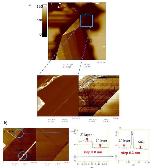
easily achieved with an adhesive tape. In particular, in 2004 Geim and Novoselov first used an adhesive tape to detach a mono-atomic graphene sheet by a mechanical cleaving technique from a piece of highly oriented pyrolytic graphite (HOPG). The authors prepared graphite flakes of few millimeters that were then compressed against a layer of wet photoresist over a glass substrate. In order to attach the graphite flakes to the photoresist layer, the samples were baked. The detachment of graphene and few layer graphene was performed using an adhesive tape to peel off the graphite flakes and then the flakes were released in acetone. The layers were firstly transfer from the acetone solution to a Si substrate (n-doped Si with a SiO2 top layer), and then cleaned with water
and propanol. The graphene layers with a thickness less than 9 nm well adhered on the Si substrate and the adherence force between graphene and the substrate was claimed to be van der
Waals and/or capillary forces. Across the years, many research groups have used this economic and facile approach to produce high quality graphene layers in order to use them for the fabrication of nanoelectronic devices. The costless and advantageous of the technique brought scientists to extend this process for fabricating other 2D materials like boron nitride (BN), molybdenum disulfide (MoS2), and niobium
diselenide (NbSe2) (84; 85). However, the mechanical
exfoliation process needs improvements for large-scale, defect-free graphene for its use in nanoelectronics.
The first year of my PhD, I focused my attention on the synthesis of graphene by mechanical exfoliation of graphite with the “scotch tape technique”. The experimental results will be discussed in the next chapter.
2.4.2. Chemical Exfoliation
Another top down approach for the synthesis of graphene is the chemical exfoliation of graphite that takes place along the normal to graphite basal plane of the original flakes. Generally, the exfoliation of graphite is achieved by the use of different kind of species that can intercalate between the graphite planes. Graphite can accept many species into the space
between graphite layer planes, in particular the species with the ionic radii smaller than the graphite interlayer spacing, can fit easily between the graphite planes to form the graphite intercalation compounds (GICs). The intercalating compounds can be classified in, donor-type intercalation compounds (e.g., K-GIC) where the intercalates donate electrons to the host graphite and acceptor-type intercalation compounds (i.e., H2SO4- and FeCl3-GICs) that accept electrons from the host
(86). For the production of graphene sheets, usually alkali metals are employed as intercalating compounds. As an example, we can mention the work of Kaner and coworkers (87), which employed the KC8 as intercalation compound. A
highly exothermic reaction between the KC8 compound and
aqueous solution of ethanol causes the exfoliation of graphite:
According to this equation, potassium ions dissolve into the solution producing the potassium ethoxide along with hydrogen gas evolution that helps in separating the graphitic layers. The filtration of the solution provides the few-layer exfoliated graphene that is then purified by washing it with ethanol.