ALMA MATER STUDIORUM - UNIVERSITÀ DI BOLOGNA
SCUOLA DI INGEGNERIA E ARCHITETTURA
DIPARTIMENTO di
INGEGNERIA DELL’ENERGIA ELETTRICA E DELL’INFORMAZIONE “Guglielmo Marconi”
DEI
CORSO DI LAUREA MAGISTRALE IN INGEGNERIA ELETTRONICA
TESI DI LAUREA
in
LAB OF DIGITAL ELECTRONICS
DESIGN OF A CLUSTER-COUPLED HARDWARE
ACCELARATOR FOR FFT COMPUTATION
CANDIDATO RELATORE
Luca Bertaccini Prof. Dr. Davide Rossi
CORRELATORI Prof. Dr. Luca Benini Dr. Francesco Conti Gianna Paulin Anno Accademico 2018/2019 Sessione III
1
Sommario
Il progetto descritto in questa tesi riguarda lo sviluppo di un acceleratore hardware per il calcolo della Fast Fourier Transform (FFT) da integrare all’interno di un cluster PULP. Il progetto è stato realizzato in parte all’Università di Bologna ed in parte presso ETH Zurich.
La piattaforma PULP (Parallel Ultra Low Power) è un progetto nato nel 2013 dalla collaborazione tra il gruppo EEES (Energy-efficient Embedded Systems) dell’Università di Bologna e l’Integrated Systems Laboratory (IIS) di ETH Zurich [1].
L’interesse verso la FFT trova motivazione nelle sue numerose applicazioni. La FFT infatti non solo viene utilizzata nell’analisi di dati ma rappresenta anche un front-end per applicazioni relative a machine learning e reti neurali. L’obiettivo di questo progetto è realizzare un acceleratore che permetta di calcolare questi tipi di algoritmi più velocemente e consumando meno potenza rispetto a realizzazioni software.
Per questo progetto è stata implementata la radix-2 DIT (Decimation-in-Time) FFT e l’intero design è stato realizzato in SystemVerilog sintetizzabile. All’interno della parte computazionale dell’acceleratore è stata utilizzata l’aritmetica Fixed-point ed il corretto funzionamento di questa unità è stato validato utilizzando alcuni script MATLAB. Tale acceleratore, essendo stato concepito per essere integrato nella piattaforma PULP, è stato progettato in accordo con i protocolli di comunicazione implementati all’interno di tale scheda. Le performance dell’acceleratore sono poi state stimate in termini di area, timing, flessibilità, e tempi di esecuzione. L’acceleratore hardware è risultato essere sette volte più veloce di un software altamente ottimizzato che calcola la FFT su 8 core. In tecnologia 22 nm, l’acceleratore occupa circa 115000 µm² ed è caratterizzato da una massima frequenza di funzionamento di 690 MHz.
Per evitare frequenti conflitti nell’accesso alla memoria esterna, un buffer è stato internalizzato all’interno dell’acceleratore. Tale scelta ha portato a più brevi tempi di esecuzione ma anche ad un notevole incremento nell’area complessiva.
Infine, è stato studiato un modo per rimuovere il buffer interno e le caratteristiche di questa architettura alternativa sono state comparate con i risultati ottenuti per la versione dell’acceleratore implementata in questo progetto di tesi.
2
Abstract
This thesis is related to the design of a hardware accelerator computing the Fast Fourier Transform (FFT) to be integrated into a PULP cluster. The project has been realized partly at the University of Bologna and partly at ETH Zurich.
PULP (Parallel Ultra Low Power) platform is a joint project between the Energy-efficient Embedded Systems (EEES) group of UNIBO and the Integrated Systems Laboratory (IIS) of ETH Zurich that started in 2013 [1].
The interest in FFT is motivated by its several applications. The FFT not only is used in data analytics but also represents a front-end for machine learning and neural networks application. The goal of this accelerator is to speed up these kinds of algorithms and to compute them in an ultra-low-power manner.
For the project described in this thesis, the radix-2 DIT (Decimation-in-Time) FFT has been implemented and the whole design has been realized in synthesizable SystemVerilog. Fixed-point arithmetic has been used within the computational part of the accelerator and the correct behavior of this unit has been evaluated making use of some MATLAB scripts. Since the accelerator has been conceived to be integrated into the PULP platform, it has been designed in compliance with the communication protocols implemented on such a board. The performance of the hardware accelerator has then been estimated in terms of area, timing, flexibility, and execution time. It has resulted to be seven times faster than a highly optimized software running FFT on 8 cores. In 22 nm technology, it occupies around 115000 µm² and it is characterized by a maximum clock frequency of 690MHz.
To avoid frequent conflicts accessing the external memory, a buffer has been internalized into the accelerator. Such a choice has led to shorter execution times but has increased considerably the overall area.
Finally, a way to remove the internal buffer has been studied and the features of this new possible design have been compared to the results obtained for the implemented version of the FFT hardware accelerator.
3
Contents
1. Introduction ... 5
1.1 Related Work ... 6
2. Fast Fourier Transform (FFT) ... 8
2.1 From DFT to FFT... 8
2.2 Radix-2 FFT ... 10
2.3 Radix-4 FFT ... 12
2.4 Radix-8 ... 14
3. Tools... 15
3.1 PULP platform & HWPEs ... 15
3.2 Protocols ... 17
3.2.1 HWPE-Stream Protocol ... 17
3.2.2 HWPE-Mem Protocol ... 18
3.3 Programming Languages & Software ... 19
3.4 Fixed-Point Arithmetic ... 20
4. FFT HWPE ... 22
4.1 Finite State Machine (FSM) ... 24
4.2 Butterfly Unit ... 26
4.2.1 Radix-2 Butterfly Unit ... 26
4.2.2 Radix-4 Butterfly Unit ... 30
4.2.3 Radix-8 Butterfly Unit ... 33
4.2.5 Butterfly Datapath ... 35 4.3 Index Generator ... 39 4.4 Buffer ... 40 4.5 Streamer ... 45 4.6 Scatter/Gather ... 46 4.7 ROM ... 47 5. Results ... 49 5.1 Hardware Results ... 49 5.2 Design Verification ... 56
4
8. Conclusion and Future Work ... 63 References ... 64
5
1. Introduction
The Fast Fourier Transform (FFT) is one of the fundamental blocks necessary to perform digital signal processing for biomedical, robotic and, in general, sensing applications. It represents as well a front-end for applications based on neural networks and machine learning. This function may be realized in software or in hardware. A hardware implementation may achieve better performance in terms of execution time and energy efficiency. Software applications are generally constrained to perform instructions serially whereas, in hardware, many tasks may be executed in parallel. Therefore a hardware implementation may lead to remarkable improvements in terms of throughput and power consumption, even if it requires a more complex design.
The aim of this project is to design a hardware accelerator performing FFT to be integrated into a PULP cluster to enhance the board performance when it is used to perform machine learning and neural network applications. Therefore the hardware accelerator has been designed to achieve high performance and flexibility with respect to these kinds of applications.
First of all, the FFT theory will be presented explaining the reasons to introduce such a transform and showing different FFT algorithms. Afterward, Hardware Processing Engines (HWPEs), a particular class of hardware accelerators conceived to be integrated into a PULP board, and their communication protocols will be described. Then the structure of such FFT HWPE will be discussed, presenting all the hardware components implemented within the design and describing their main features. The obtained results in terms of area, timing, and execution time will be shown and compared to the performance of a highly optimized software running FFT on 8 cores. Such software was provided by GreenWaves Technology. Finally, an alternative architecture has been studied and compared to the implemented one.
6
1.1 Related Work
Many implementations of FFT hardware accelerators may be found in the literature. The particularity of the accelerator described in this thesis is given by the platform addressed. It has been conceived in compliance with the protocols used within PULP and with the hardware constraints introduced by such an environment. Moreover, the accelerator has been designed to be able to work with different data sizes and different numbers of FFT points.
Slade provided an architecture for a FFT FPGA implementation [2]. His design has been taken as a reference to develop the hardware accelerator. However, the accelerator realized for this thesis project is an IP conceived to be integrated into a SoC and hence a different design approach has been considered. Furthermore, Slade’s implementation worked just with 16-bit complex data (16 bits for the real part and 16 bits for the imaginary part), while this hardware accelerator may work also with 8/32-bit complex values.
For this accelerator, a buffer has been internalized to store partial results and to avoid several memory conflicts. This kind of memory-based approach has been inspired by the work of Wang et al [3]. Their architecture might also handle 2𝑛3𝑚5𝑘 FFT points, while this accelerator will compute just 2𝑛 FFT points.
At the end of the project, a new possible architecture without the internal buffer has been proposed. This new solution finds its fundament on the work of Xiao et al [4]. Since the samples needed for a butterfly are most of the time stored in the same memory bank, the basic idea is to set one address and read data from multiple memory banks. Afterward, the data are stored in some registers, waiting for the other samples necessary to compute the correspondent butterfly. Xiao et al applied this approach to 4 FFT, it has then been extended to radix-2 FFT for the purpose of this project. Another way to avoid memory conflicts without the implementation of an internal buffer is presented by Johnson [5]. He proposed an in-place approach that stored the butterfly outputs in a permutation of the memory locations related to the butterfly inputs.
Within this hardware accelerator, the Cooley-Tuckey algorithm [6] has been implemented. Radix-2/4/8 FFT [7][8] have been evaluated, as well as a pipeline architecture able to compute these three different radices [9]. The area/timing trade-off of the related butterfly units and the computational complexity of such algorithms have been considered. Furthermore, the
7
connections among the various algorithms and the differences in terms of performance have been highlighted. Finally, the radix-2 approach has been selected.
The butterfly unit has then been realized in fixed-point arithmetic. An overview of the FFT algorithm computed implementing such arithmetic may be found in [10]. To design this module Welch’s work [11] and Kabal and Sayar’s study [12] have been fundamental. The magnitude of the complex values grows by up to a factor of two across a butterfly and Welch provided some approaches to manage such growth, maintaining the same data size at the input and at the output of the butterfly unit. For this project, it has been chosen to provide the butterfly module with complex data less than 0.5 in modulus and to perform a right shift at the end of the butterfly computation. In this way, since the outputs will represent the inputs in the next FFT stage, the inputs are always less than 0.5 in modulus across the FFT computation. Kabal and Sayar studied how different rounding operations inside the butterfly affected the FFT results, trying to find a way to minimize the error. Since one multiplication is required for the radix-2 butterfly computation, the result of such an operation should be represented with two times the number of bits used for the factors. If it is required to maintain the same word length at input and output, half of the number of bits utilized for the product has to be discarded and at this point, a rounding operation is implemented to minimize the error committed.
For the index generator design, some counters have been used, exploiting the regularities that characterize the FFT. Another manner to compute those indices using one counter and some logical operation is shown by Cohen [13].
Finally, since this accelerator has been conceived to be integrated into PULP, a hardware accelerator designed for PULP computing a MAC operation [14] and its testbench [15] have been studied. When designing an accelerator for the PULP platform some reusable modules, as the streamer [16], which is basically a specialized DMA unit, and the interface with the register file [17] may be implemented. Such modules have been studied and adapted for the design of the FFT accelerator.
8
2. Fast Fourier Transform (FFT)
In this section, the FFT theory is presented. First of all, the reasons to define this kind of algorithm are discussed, then the Cooley-Tuckey FFT algorithm [6] is presented and some considerations regarding its inputs and outputs are shown. Finally, three FFT algorithm, the radix-2/4/8 FFT, are described.
2.1 From DFT to FFT
The Fourier Transform (FT) converts a signal from a time domain to a continuous-frequency domain and is defined as:
In digital signal processing, we deal with signals sampled over a finite time interval and thus we need a transform able to convert a signal from a discrete-time domain to a discrete-frequency domain. Such a function is called Discrete Fourier Transform (DFT) and it is defined as:
where N is the number of samples and 𝑊𝑁𝑛𝑚 = 𝑒−𝑖 2𝜋
𝑁𝑛𝑚 are the so-called twiddle factors.
Since DFT works on a finite set of data, it may be implemented in computers or dedicated hardware. Nevertheless, the computational complexity of the DFT, 𝑂(𝑁2), makes it too costly to compute it applying the definition. Instead of the DFT, the Fast Fourier Transform (FFT) is normally utilized, which is basically an optimized way of calculating the DFT. The most common FFT is the Cooley-Tuckey algorithm. This is based on a Divide et Impera approach, which recursively breaks down a DFT into smaller DFTs.
Radix-r FFT divides the summation recursively in r parts. As r increases more data must be processed concurrently and the selection of such data becomes more and more complex. The algorithm is considerably simpler when r is a power-of-two. For all these reasons the most used Radix-r FFT algorithms are the radix-2, radix-4, and radix-8 FFT. To be effective, a Radix-r FFT must work on vectors whose sizes are power-of-r. Therefore when this requirement is not met, a zero-padding operation is performed. Such an operation simply adds some zeros at the
𝑋(𝑓) = ∫ 𝑥(𝑡)𝑒−𝑖2𝜋𝑓𝑡𝑑𝑡 +∞ −∞ (2.1.1) 𝑋𝑚 = ∑ 𝑥𝑛 𝑁−1 𝑛=0 𝑊𝑁𝑛𝑚 , 𝑚 = 0,1, . . . , 𝑁 (2.1.2)
9
end of the vector of samples to bring its size to a power-of-r. To understand how this procedure affects the FFT outcome, it is necessary to study in greater detail the meaning of the FFT results.
The “FFT Tutorial” [18] provides a good introduction to the FFT and its meaning. While a good explanation of the zero-padding effect on the resulting spectrum is available at
http://www.bitweenie.com/listings/fft-zero-padding/ [19].
Two important characteristics of a FFT spectrum must be considered. The first one is the minimum spacing between two frequencies that can be resolved which is computed as:
where T is the time length of the signal with data. The second one corresponds to the distance between two FFT bins in the spectrum and it is defined as
which is proportional to the number of FFT points.
Hence, the time length of the signal with data should be large enough that 1 𝑇⁄ is smaller than the minimum spacing between frequencies of interest. Furthermore, there should be enough FFT points so that the frequencies of interest are not split between multiple FFT bins.
Therefore, if there are already enough FFT points to show in the spectrum the FFT frequencies we can solve, adding some zeros does not modify the resulting spectrum. The information contained in the FFT results is proportional to the time length of the signal with data (it does not consider the zeros padded).
∇𝑊𝐹𝑅 = 1
𝑇 (2.1.3)
∇𝑅 = 𝑓𝑠 𝑁𝐹𝐹𝑇
10
2.2 Radix-2 FFT
The radix-2 FFT is the most common FFT algorithm. It divides the summation into two parts recursively. There are two main ways to implement it. The first one is the Decimation-In-Frequency (DIF) approach and the second one is the Decimation-In-Time (DIT). Both of them lead to a computation complexity of 𝑂(𝑁𝑙𝑜𝑔2𝑁), which represents a remarkable improvement
if we compare it with the DFT computational cost 𝑂(𝑁2).
The DIF approach divides recursively the summation in the following way:
It is characterized by a processing flow of the following type:
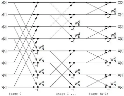
Figure 1: 8-point DIF FFT
As it can be noticed by Figure 1, implementing the DIF algorithm requires to work with inputs in natural order and outputs in bit-reversed order.
While the DIT approach divides the summation in the following way: 𝑋𝑚 = ∑ 𝑥𝑛 𝑁 2−1 𝑛=0 𝑊𝑁𝑛𝑚+ 𝑊 𝑁 𝑚𝑁2 ∑ 𝑥𝑛+𝑁 2 𝑁 2−1 𝑛=0 𝑊𝑁𝑛𝑚 , 𝑚 = 0,1, . . . , 𝑁 − 1 (2.2.1) 𝑋𝑚 = ∑ 𝑥2𝑛 𝑁 2−1 𝑛=0 𝑊𝑁2𝑛𝑚+ 𝑊𝑁𝑚 ∑ 𝑥2𝑛+1 𝑁 2−1 𝑛=0 𝑊𝑁2𝑛𝑚 , 𝑚 = 0,1, . . . , 𝑁 − 1 (2.2.2)
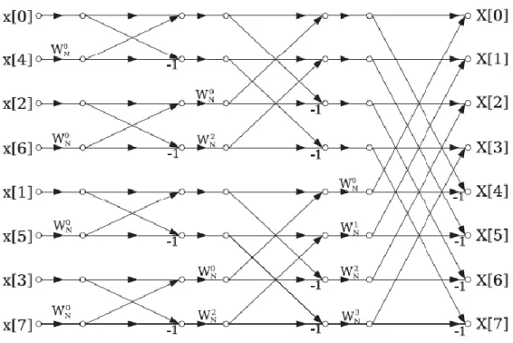
11 The DIT FFT diagram for an 8-point input vector is:
Figure 2: 8-point DIT FFT
In this case, the inputs are in bit-reversed order, while the outputs are in natural order. This second approach has been implemented for the project described in this thesis.
It can be noticed that a basic operation called Butterfly is iterated multiple times within the processing. Such an operation is made of one complex multiplication, one complex addition, and one complex subtraction.
Figure 3: Radix-2 Butterfly
{𝑦[0] = 𝑥[0] + 𝑤 ∗ 𝑥[1]
12
Some regularities in the processing flow of the DIT approach can also be observed. For a 2𝑛
-point radix-2 FFT:
As regards twiddle factors, it may be noticed that just N/2 different twiddle factors are necessary thanks to the symmetry of the computation. The value of the twiddle factor exponent also varies regularly. Starting from the last stage and moving towards the first stage the difference between one twiddle factor exponent and the following one is 1, 2, 22, 23,…. In the first stage, all the
twiddle factors exponents are zero, which is like having a difference of 2n−1 considering a
(𝑛 − 1)-bit counter and taking into account that we deal with just N/2 different twiddle factors.
2.3 Radix-4 FFT
Radix-4 FFT divides the DFT summation into four parts recursively. Also, in this case, a Decimation-In-Frequency (DIF) and a Decimation-In-Time (DIT) approach may be implemented. Just the DIT algorithm will be presented in this section. An overview of such an algorithm is provided by Douglas L. Jones [7].
Radix-4 FFT leads to a computation complexity of 𝑂(𝑁𝑙𝑜𝑔4𝑁), which represents an even better improvement than the one introduced by the radix-2. However, it leads to a more complex butterfly and control unit. Furthermore, Radix-4 FFT requires to work with numbers of FFT points that are powers-of-4.
The radix-4 DIT algorithm divides recursively the summation in the following way: Distance between butterfly inputs Butterflies per stage Stages Total # Butterflies Butterfly groups Butterflies per group 1, 2 , 22, …, 2n−1 2n−1 n 2n−1∗ n 2n−1, …, 22, 2 , 1 1, 2 , 22, …, 2n−1 𝑋𝑚 = ∑ 𝑥4𝑛 𝑁 4−1 𝑛=0 𝑊𝑁4𝑛𝑚+ 𝑊𝑁𝑚∑ 𝑥4𝑛+1 𝑁 4−1 𝑛=0 𝑊𝑁4𝑛𝑚+ 𝑊𝑁2𝑚 ∑ 𝑥4𝑛+2 𝑁 4−1 𝑛=0 𝑊𝑁4𝑛𝑚 + 𝑊𝑁3𝑚∑ 𝑥4𝑛+3 𝑁 4−1 𝑛=0 𝑊𝑁4𝑛𝑚 , 𝑚 = 0,1, . . . , 𝑁 − 1 (2.3.1)
13
It is characterized by a processing flow of the following type:
Figure 4: DIT Radix-4 FFT
Figure 5: Radix-4 DIT Butterfly
Computing one radix-4 butterfly is like calculating two steps of two radix-2 butterflies, which are four radix-2 butterflies. However, the radix-4 FFT has a computational advantage because fewer arithmetic operations are required. Three complex multiplications instead of four are needed.
14
2.4 Radix-8
Radix-8 FFT divides the DFT summation into eight parts recursively and leads to a computation complexity of 𝑂(𝑁𝑙𝑜𝑔8𝑁). As the Radix-4 FFT, the Radix-8 FFT improves the computation complexity but leads also to a more complex design. Furthermore, Radix-8 FFT requires to work with numbers of FFT points that are powers-of-8.
The radix-8 DIT algorithm divides recursively the summation in the following way:
Computing one radix-8 butterfly is like calculating three steps of four radix-2 butterflies, hence it is like computing twelve radix-2 butterflies. Also in this case, there is a computational advantage because fewer arithmetic operations are required.
A comparison of these three different algorithms, radix-2/4/8 FFT, is given by Jayakumar and Logashanmugam [8]. 𝑋𝑚 = ∑ 𝑥8𝑛 𝑁 8−1 𝑛=0 𝑊𝑁8𝑛𝑚+ 𝑊𝑁𝑚∑ 𝑥8𝑛+1 𝑁 8−1 𝑛=0 𝑊𝑁8𝑛𝑚+ 𝑊𝑁2𝑚 ∑ 𝑥8𝑛+2 𝑁 8−1 𝑛=0 𝑊𝑁8𝑛𝑚 + 𝑊𝑁3𝑚∑ 𝑥8𝑛+3 𝑁 8−1 𝑛=0 𝑊𝑁8𝑛𝑚+ 𝑊𝑁4𝑚∑ 𝑥8𝑛+4 𝑁 8−1 𝑛=0 𝑊𝑁8𝑛𝑚 + 𝑊𝑁5𝑚∑ 𝑥8𝑛+5 𝑁 8−1 𝑛=0 𝑊𝑁8𝑛𝑚+ 𝑊𝑁6𝑚∑ 𝑥8𝑛+6 𝑁 8−1 𝑛=0 𝑊𝑁8𝑛𝑚 + 𝑊𝑁7𝑚∑ 𝑥 8𝑛+7 𝑁 8−1 𝑛=0 𝑊𝑁8𝑛𝑚 , 𝑚 = 0,1, . . . , 𝑁 − 1 (2.4.1)
15
3. Tools
In this section, the Hardware Processing Engines and the protocols implemented within the PULP board are introduced. Afterward, an overview of the main software and programming languages utilized for the project is presented. Finally, fixed-point arithmetic is discussed.
3.1 PULP platform & HWPEs
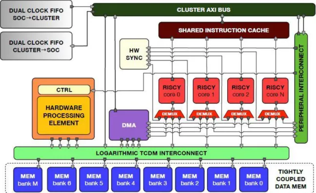
A cluster-coupled Hardware Processing Engine (HWPE) is a hardware accelerator conceived to be integrated into a PULP cluster, which shares the L1 memory with the cores and which is software controlled via a memory-mapped peripheral port.
Figure 6: PULP CLUSTER & HWPE
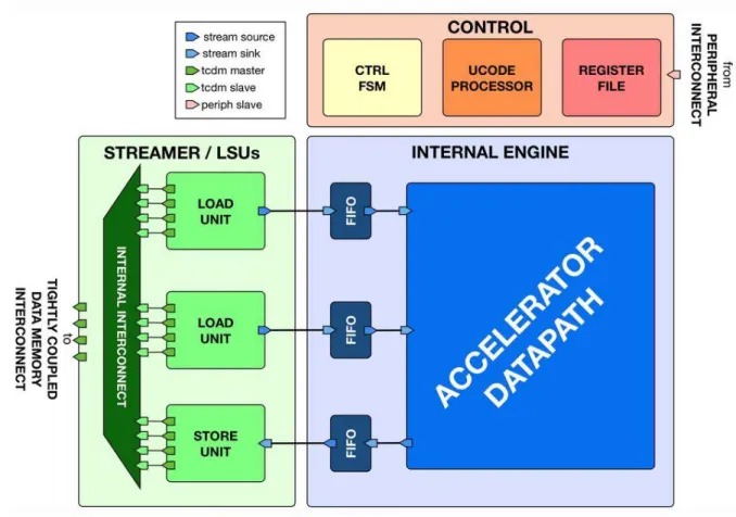
HWPEs, as hardware accelerators are intrinsically application-specific, but since they are meant to be integrated into a PULP cluster, some blocks can be reused within the design of such accelerators. These reusable modules are related to the interface with the PULP cluster Tightly-Coupled Data Memory (data streams) [16] or a core (control) [17]. The datapath is instead always application-specific.
16
Figure 7: HWPE structure
The PULP platform also introduces some constraints. The accelerator will be interfaced with a 64 KB memory and will be characterized by a bandwidth of 128 bits.
The main reusable blocks used for HWPE design are presented at
17
3.2 Protocols
The HWPE protocols are briefly discussed in this section. All the details related to such protocols are available at https://hwpe-doc.readthedocs.io/en/latest/ [20].
3.2.1 HWPE-Stream Protocol
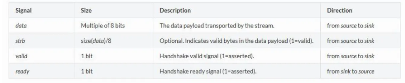
The HWPE-Stream Protocol is a protocol conceived to be used to move data between sub-components of a HWPE. In Figure 7 such a protocol is employed in the communication between the datapath and the streamer. HWPE-Stream streams are directional and flow from a source to a sink, implementing a handshake based on two signals (valid, ready). They carry a data payload in the signal data. Signal strb indicates valid bytes inside data, while valid and ready are used to validate the transaction.
Figure 8: HWPE-Stream Protocol
Figure 9: HWPE-Stream Signals
Transactions must respect the following rules:
1. A handshake happens in the cycle when both valid and ready are 1;
2. data and strb can change their value either after a handshake or when valid is 0;
3. The transition 0 to 1 of valid cannot depend combinationally on ready, but the transition 0 to 1 of ready can depend combinationally on valid;
18
3.2.2 HWPE-Mem Protocol
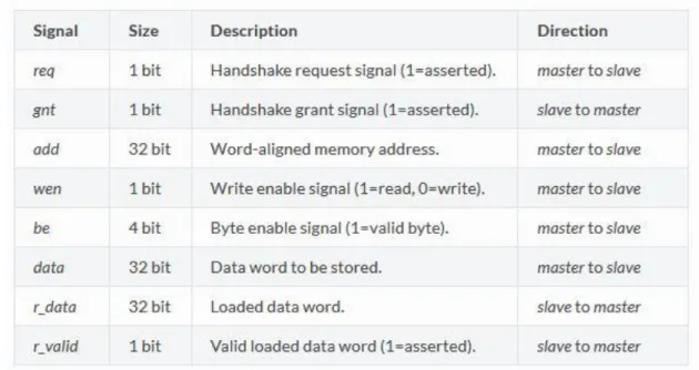
HWPE-Mem Protocol is used to move data between the HWPE and the L1/L2 external memory. It implements a simple request/grant handshake. In Figure 7 such a protocol is utilized between the streamer and the Tightly-Coupled Data Memory (TCDM).
Figure 10: HWPE-Mem Protocol
The HWPE-Mem protocol is directional and connects a master to a slave. Signal req and gnt are used for the handshake. Transactions must respect the following rules:
1. A handshake occurs when valid and req are set to 1.
2. r_valid must be set to 1 after a valid handshake and r_data must be valid on that cycle. 3. The transition 0 to 1 of req cannot depend combinationally on gnt, while the transition
from 0 to 1 of gnt can depend combinationally on req.
There is also another version of the HWPE-Mem Protocol called HWPE-MemDecoupled. In such a protocol rule 2 is substituted by a rule 4:
19
Figure 11: HWPE-Mem Signals
3.3 Programming Languages & Software
SystemVerilog: The hardware programming language used for the whole design of the hardware accelerator is synthesizable SystemVerilog. Sutherland S. and Mills D [21] provide a manual for basic SystemVerilog that has been taken as a reference.
Git: Git, as a control-version system, has been used to manage the project and its various versions. Some tutorials related to this tool are available at https://git-scm.com/[22].
MATLAB: Some scripts have been realized in MATLAB to verify the correct behavior of the design. In particular, one script has been coded for the FFT computation in double precision to assess the information loss and another script has been designed for the bit-true implementation of the FFT, which is a software version of the function realized in hardware.
Synopsys Design Compiler: it has been used to synthesize the design to find some results in terms of area and timing.
20
3.4 Fixed-Point Arithmetic
The computational part of the hardware accelerator has been realized in fixed-point arithmetic. Randy Yates [23] and the set of slides provided by the University of Washington [24] provide an overview of such arithmetic, which is widely employed in Digital Signal Processors (DSPs).
A set of N bits is characterized by 2𝑁 possible states. However, the meaning of a binary word depends completely on its interpretation.
Fixed-point values are basically integers scaled by an implicit factor. Thus, with this kind of data, it is possible to represent rational numbers. Once the scaling factor is fixed, a subset of 2𝑁 rational numbers can be expressed. If the binary word is interpreted as a signed two’s complement fixed-point rational the subset of rational numbers is:
where b is the number of fractional bits. Since we are representing rational values with a finite set of bits, there may be a difference between the real value and its representation. The maximum error that may be committed will be half of the smallest non-zero magnitude representable.
The range of this representation is given by:
Therefore a 8-bit word with three fractional bits will have the form:
where the MSB is employed as a sign bit.
Often a Q-format notation is implemented to give information regarding the number of fractional and integer bits. Qx.y means that the word is characterized by x integer bits and y fractional bits. If we are dealing with a signed word, the total number of bits will be x+y+1.
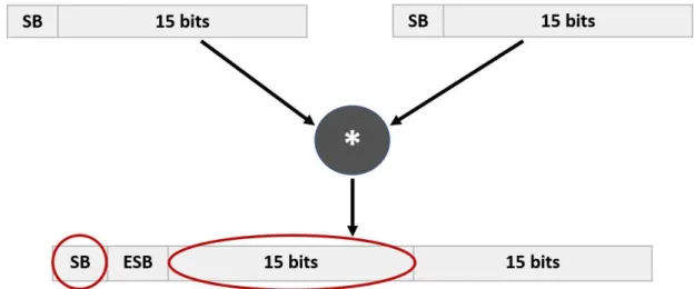
Within this project, the accelerator will work with normalized signed numbers. Hence, the values will be of the type Q0.y. The multiplication of two Q0.y numbers will lead to a Q0.2y result where the two MSBs are the sign bit (SB) and the extension sign bit (ESB). Since the word length will be maintained for input/output, the product will be restored to a Q0.y notation. 𝑃 = {𝑝/2𝑏 | −2𝑁−1≤ 𝑝 ≤ −2𝑁−1− 1, 𝑝 ∈ 𝑍} (3.4.1)
−2𝑁−1−𝑏 ≤ 𝑝 ≤ +2𝑁−1−𝑏− 1/2𝑏 (3.4.2)
21
To realize that, it is sufficient to discard the extension sign bit and the last y bits. Proceeding in this way implies a rounding/truncation in the results since the y LSBs are lost.
If we consider the multiplication of two 16-bit words in the format Q0.15, we find:
22
4. FFT HWPE
To design this HWPE, the Hardware MAC Engine (
https://github.com/pulp-platform/hwpe-mac-engine [14]), its testbench (https://github.com/pulp-platform/hwpe-tb[15]) and a FPGA
implementation of the FFT [2] have been taken as reference.
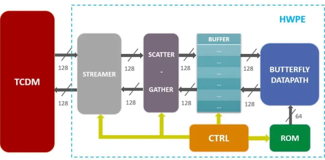
This particular HWPE is conceived for the FFT computation. To realize that function the following hardware blocks have been implemented:
1. STREAMER: a specialized DMA unit, it represents the accelerator interface towards the memory;
2. SCATTER/GATHER: when data are read from the Tightly Coupled Data Memory (TCDM) the streamer passes them to the scatter, which decides where to store the data inside the buffer; when data must be stored into the TCDM, the gather collects the data from the buffer and passes them to the streamer;
3. BUFFER: an internalized memory is used to store all the FFT samples; when the data are processed by the butterfly unit, the inputs come from the buffer and the outputs overwrite the samples in the buffer;
4. BUTTERFLY UNIT: it implements the basic operation that is iterated to compute the FFT;
5. CONTROLLER (Index Generator, FSM, interface with the register file): the FSM controls the whole processing. When data are processed using the butterfly unit, the index generator selects the right samples in the buffer and the right twiddle factors from the ROM to feed the butterfly unit. The number of FFT points, the data size and the base address of the vector inside the TCDM are written via software into the register file and then read by the controller.
23
The structural scheme of the accelerator is the following:
Figure 13: FFT HWPE structural scheme
As it can be noticed by Figure 13, all the components that deal with the samples work with two 32-bit complex data per cycle, which means 128 bits. While the ROM provides the Butterfly Datapath with 64 bits, which represent 4/2/1 twiddle factors, respectively for 8/16/32-bit complex data.
24
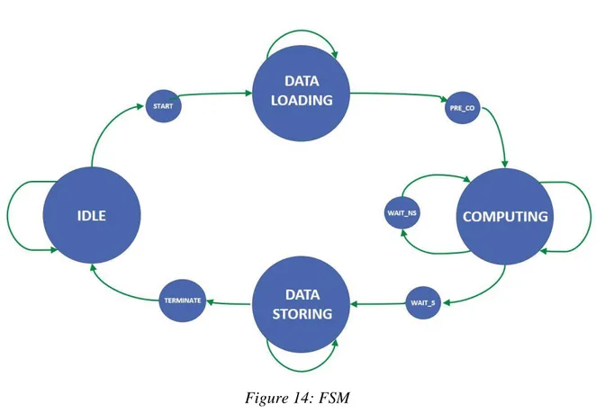
4.1 Finite State Machine (FSM)
Figure 14: FSM
The processing is controlled by a simple Finite State Machine (FSM), composed of nine states:
• IDLE;
• START: in this state the streamer and the scatter are initialized for the load;
• DATA_LOADING: all the FFT samples are read from the TCDM and stored into the buffer, passing through the scatter;
• PRE_COMPUTING (PRE_CO in Figure 14): in this state, the index generator is initialized;
• COMPUTING: the controller selects the right samples in the buffer and the right twiddle factors from the ROM to feed the butterfly unit, which processes the data. Afterward, its outputs are stored into the buffer overwriting the input samples. Such an operation is iterated multiple times;
• WAIT_FOR_NEW_STAGE (WAIT_NS in Figure 14): Since the inputs and the outputs of the butterfly datapath are registered to break the critical path, the results of a butterfly are stored two cycles after the input samples are read from the butterfly. This state is used to introduce a two-cycle delay after having read all the input samples from the buffer. In this way, read after write (RAW) data hazard are avoided because the
25
accelerator waits for all the stage results to be stored into the buffer before starting reading the new samples;
• WAIT_STORE (WAIT_S in Figure 14): in this state, the gather and the streamer are initialized for the following store;
• DATA_STORING: all the FFT results are inside the buffer and now the accelerator may store all of them into the TCDM, passing through the gather and the streamer. In this state, the gather arranges the data in streams and passes them to the streamer who starts to store them into the TCDM;
• TERMINATE: The DATA_STORING state ends when all the data are passed to the streamer by the gather. In this state, the accelerator waits for all the results to be written into the TCDM.
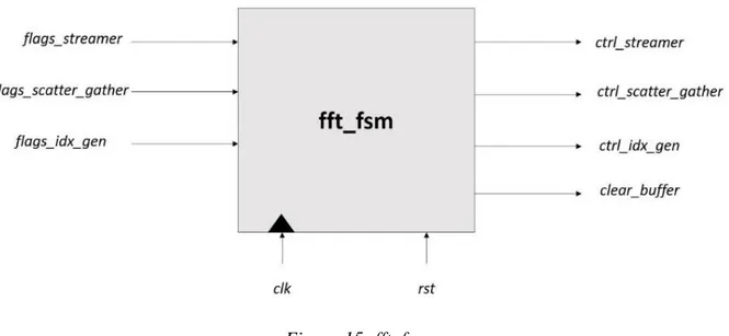
Figure 15: fft_fsm
The FSM basically receives flags from the other components and sends them back control signals.
26
4.2 Butterfly Unit
The Butterfly Unit represents the FFT HWPE datapath. Since its bandwidth is 128 bits, which can represent 8/4/2 complex samples respectively for 8/16/32-bit complex data, the datapath could be provided with the necessary inputs to compute either 8-bit radix-2/4/8 butterflies or 16-bit radix-2/4 butterflies or 32-bit radix-2 butterfly.
The Decimation-In-Time approach has been implemented within this project.
4.2.1 Radix-2 Butterfly Unit
Figure 16: Radix-2 Butterfly
The main characteristics of the radix-2 butterfly unit are the following:
• The module works with normalized numbers, expressed through fixed-point notation (Q0.7/15/31 respectively for 8/16/32-bit complex data);
• The magnitude of the complex values grows by up to a factor of two across a butterfly. To prevent overflow, some solutions are proposed by Peter D. Welch [11]. For this project, it has been chosen to require the butterfly inputs to be less than 1/2 in modulus. Proceeding in this way it is ensured that the outputs will be less than 1 and hence that there will be no overflow;
• At the end of the computation, the butterfly unit right-shifts the outputs by one bit to scale by 1/2 and ensures that at the next iteration the inputs will still be less than 1/2 (Such scaling is not performed during the last iteration).
• To compute the radix-2 butterfly, one complex multiplication and two complex additions are performed. Therefore the outputs should be represented with more bits with respect to inputs, in order not to lose information. However, the outputs of a butterfly will represent the inputs of another butterfly in the following stage, hence the same amount of bits has been assigned to inputs and outputs. Some rounding operations
27
have been realized to minimize information loss. A deeper analysis of the possible rounding operation is provided by P. Kabal and B. Sayar [12].
• Inputs and outputs are registered.
The module was then synthesized with Synopsys to obtain some results in terms of area and timing, varying the data size of the real and imaginary part (8/16/32).
For 8-bit complex samples, the results are the following:
Figure 17: Area/Timing Tradeoff, 8-bit Radix-2 Butterfly
T_clk f_clk Combinational Area [µm²] Total Cell Area [µm²] Slack [ps]
1000 ps 1 GHz 473 608 MET 750 ps 1,33 GHz 507 643 MET 500 ps 2 GHz 509 646 MET 450 ps 2,22 GHz 547 688 MET 405 ps 2,47 GHz 744 890 MET 400 ps 2,5 GHz 724 873 -3 350 ps 2,86 GHz 757 909 -54 250 ps 4 GHz 844 998 -148
A negative slack informs us that the critical path exceeded the fixed clock cycle. When the slack is negative, the plotted values correspond to a clock_period = T_clk + |slack|.
500 600 700 800 900 1000 1100 300 400 500 600 700 800 900 1000 1100 To ta l Ce ll Are a [µ m ²] T_clk [ps]
Area-Timing Tradeoff
Radix-2 Butterfly, DATA_SIZE = 8
28 While for 16-bit complex samples:
Figure 18: Area/Timing Tradeoff, 16-bit Radix-2 Butterfly
T_clk f_clk Combinational Area
[µm²]
Total Cell Area [µm²] Slack [ps] 1200 ps 0,83 GHz 1664 1934 MET 1000 ps 1 GHz 1720 1988 MET 750 ps 1,33 GHz 1766 2036 MET 550 ps 1,82 GHz 1885 2168 MET 500 ps 2 GHz 2589 2884 -3 400 ps 2,5 GHz 2914 3216 -97 300 ps 3,33 GHz 2908 3211 -192 1600 1800 2000 2200 2400 2600 2800 3000 3200 3400 300 400 500 600 700 800 900 1000 1100 1200 1300 To ta l Ce ll Are a [µ m ²] T_clk [ps]
Area-Timing Tradeoff
29 Finally for 32-bit complex data:
Figure 19: Area/Timing Tradeoff, 32-bit Radix-2 Butterfly
T_clk f_clk Combinational
Area [µm²]
Total Cell Area [µm²] Slack [ps] 1400 ps 0,7143 GHz 6270 6809 MET 1200 ps 0,833 GHz 6344 6884 MET 1000 ps 1 GHz 6480 7025 MET 750 ps 1,333 GHz 6482 7033 MET 600 ps 1,667 GHz 7397 7982 MET 550 ps 1,818 GHz 9418 10021 -30 400 ps 2,5 GHz 9612 10215 -180 6000 6500 7000 7500 8000 8500 9000 9500 10000 10500 300 500 700 900 1100 1300 1500 To ta l Ce ll Are a [µ m ²] T_clk [ps]
Area-Timing Tradeoff
30
4.2.2 Radix-4 Butterfly Unit
Radix-4 algorithms have a computational advantage over 2 algorithms because one radix-4 butterfly performs the work of four radix-2 butterflies, and requires only three complex multiplications instead of the four complex multiplications carried out by four radix-2 butterflies.
The main characteristics of the radix-4 butterfly module are the following:
• The module works with normalized complex numbers, expressed through fixed-point notation;
• The magnitude of the complex values grows by at most a factor of four across a radix-4 butterfly. Therefore It was set as a requirement that the radix-radix-4 butterfly will receive inputs that are lesser than 1/4 in modulus. Proceeding in this way it is ensured that the outputs will be less than 1 and hence that there will be no overflow;
• At the end of the computation, the radix-4 butterfly unit shifts the outputs by two bits to scale by 1/4, ensuring that at the next iteration the inputs will still be less than 1/4 (Such scaling is not performed during the last iteration);
• Also, in this case, the same amount of bits was assigned to inputs and outputs. Some rounding operations were realized to minimize information loss;
• At the end of the computation, the outputs are shifted by two bits. The results are rounded before shifting. When the two LSBs of the output are '11’, “output + 1” is shifted by two bits. Before proceeding in this way, it is checked that the “+1” operation does not lead to an overflow;
31
A Synopsys synthesis was run for 8/16-bit complex data since we need four samples each cycle to perform the radix-4 and for the 32-bit case four samples would exceed the 128 bits of bandwidth:
Figure 20: Area/Timing Tradeoff, 8-bit Radix-4 Butterfly
T_clk f_clk Combinational Area
[µm²]
Total Cell Area [µm²] Slack [ps] 1200 ps 0,83 GHz 1872 2168 MET 1000 ps 1 GHz 2312 2607 MET 750 ps 1,33 GHz 2359 2656 MET 600 ps 1,67 GHz 2468 2777 MET 550 ps 1,82 GHz 3200 3526 MET 500 ps 2 GHz 3841 4186 -15 400 ps 2,5 GHz 4127 4475 -110 1500 2000 2500 3000 3500 4000 4500 5000 400 500 600 700 800 900 1000 1100 1200 1300 To ta l Ce ll Are a [µ m ²] T_clk [ps]
Area-Timing Tradeoff
Radix-4 Butterfly, DATA_SIZE = 8
32
Figure 21: Area/Timing Tradeoff, 16-bit Radix-4 Butterfly
T_clk f_clk Combinational Area
[µm²]
Total Cell Area [µm²] Slack [ps] 1200 ps 0,83 GHz 6934 7527 MET 1000 ps 1 GHz 6979 7573 MET 850 ps 1,18 GHz 6190 7589 MET 750 ps 1,33 GHz 7398 8002 MET 650 ps 1,54 GHz 9412 10069 MET 600 ps 1,67 GHz 11400 12091 -10 500 ps 2 GHz 11195 11882 -119 5500 6500 7500 8500 9500 10500 11500 12500 400 500 600 700 800 900 1000 1100 1200 1300 To ta l Ce ll Are a [µ m ²] T_clk [ps]
Area-Timing Tradeoff
33
4.2.3 Radix-8 Butterfly Unit
The radix-8 butterfly unit design and its main features are comparable to the other butterflies shown above. A Synopsys synthesis was run just for the 8-bit case since it is the only case in which we can provide the datapath with 8 samples in one cycle.
Figure 22: Area/Timing Tradeoff, 8-bit Radix-8 Butterfly
T_clk f_clk Combinational Area
[µm²]
Total Cell Area [µm²] Slack [ps] 1400 ps 0,71 GHz 8053 8671 MET 1200 ps 0,83 GHz 8089 8710 MET 1000 ps 1 GHz 7657 8280 MET 900 ps 1,11 GHz 7422 8053 MET 800 ps 1,25 GHz 8363 9024 MET 750 ps 1,33 GHz 10244 10932 -11.3 650 ps 1,54 GHz 10368 11059 -110 7000 7500 8000 8500 9000 9500 10000 10500 11000 11500 600 700 800 900 1000 1100 1200 1300 1400 1500 To ta l Ce ll Are a [µ m ²] T_clk [ps]
Area-Timing Tradeoff
Radix-8 Butterfly, DATA_SIZE = 8
34
4.2.4 Pipelined Butterfly Unit
Finally, a pipeline implementation computing radix-2/4/8 using just radix-2 units have been studied. Such a solution has been introduced by Jungmin Park [9].
Figure 23: Pipeline Implementation of the Butterfly
Twelve radix-2 butterfly units are instantiated for such a solution. A radix-4 butterfly is computed using two-stage of two radix-2 units:
• The first stage is composed of two radix-2 units which are provided with the four inputs of the radix-4 butterfly after a permutation. Their outputs will then represent the inputs of the other two radix-2 modules;
• The second stage is composed of two radix-2 units whose inputs are the outputs of the first stage of radix-2 units. Their outputs are the outputs of the radix-4 butterfly;
• Since the radix-4 butterfly requires three twiddle factors and four radix-2 are characterized by four twiddle factors, some simple operations are realized to obtain the four twiddle factors from three twiddle factors that are provided as inputs.
These two parts of the system may be separated to realize a two-stage pipeline.
While a radix-8 butterfly unit may be realized using twelve radix-2 butterflies:
• Twelve radix-2 modules are organized in three stages of four radix-2 butterflies. Each stage feeds with its outputs (after a permutation) the following stage. The first-stage
35
inputs are the radix-8 module inputs and the last-stage outputs are the radix-8 unit outputs.
• Twelve radix-2 modules are characterized by twelve twiddle factors while a radix-8 butterfly requires just seven twiddle factors. Therefore some pre-processing is realized to obtain the twelve needed twiddle factors from the seven twiddle factors that are provided as inputs. In this phase, 6 complex multiplications are required.
Therefore we expect this new block to be characterized by worse performance than the other radix-8 butterfly unit, however, it could be easily pipelined since it reuses radix-2 units.
4.2.5 Butterfly Datapath
After having studied all these possible solutions, the radix-2 implementation was selected and a module composed of four 8-bit butterflies, two 16-bit butterflies, and one 32-bit butterfly has been designed. The reasons for such a choice are the following:
• Implementing all the different types of radix would lead to a large area and the majority of this area will be unused during the processing cycles because all the units related to different data sizes or radix will be discarded;
• This implementation removes the improvements introduced by radix-4/8 over radix-2 since it uses radix-2 units to compute radix-4/8 butterflies. Furthermore, also in this case, many modules would be unused. For example, if we need to compute a 32-bit radix-2 butterfly just one butterfly would be used.
Therefore the FFT HWPE datapath simply performs the radix-2 butterfly.
Figure 24: Radix-2 Butterfly
Three different instantiations of the butterfly unit depending on the data size (Figure 25,26,27) have been implemented. These three blocks are purely combinational. Since we need to cover
36
the cases of 8/16/32-bit complex data (8/16/32 bits for the real part and 8/16/32 bits for the imaginary part), the overall datapath interface will be related to the larger case, which is the 32-bit complex data. Maintaining that interface we can provide the datapath with all the necessary data for the computation of either one 32-bit butterfly, or two 16-bit butterflies or four 8-bit butterflies. Therefore, to fully exploit the bandwidth, the datapath will be composed of one 32-bit butterfly unit, two 16-32-bit butterfly units, and four 8-32-bit butterfly units. Another input signal will be added, data_size, which will communicate to the datapath which data size to consider, so that it will be able to select the right butterfly units needed for the current computation. Finally, some registers have been added at the input and at the output of the datapath to break the combinational path. The structure of the datapath is shown in Figure 28, where x[0] and x[1] are the output of registers and y[0] and y[1] are input of registers, while end_stage_flag is propagated to every butterfly unit. In Figure 28, just the management of the input/output samples is shown, the same operations are applied to the twiddle factors.
Figure 25: 8-bit butterfly unit
37
Figure 27: 32-bit butterfly unit
Basically, the datapath receives two 32-bit complex samples which can contain the information of either two 32-bit complex samples or two 16-bit complex samples or four 8-bit complex samples. Based on the data_size value, it rearranges the inputs to words with the right data size and selects the right butterfly units setting the input of all the other butterflies to zero. Then the results of the butterflies related to the same data sizes are concatenated to come back to two 32-bit complex words. Proceeding in this way, the outputs of the butterflies will be all zeros, except for the selected butterflies. Hence an OR operation on the butterfly outputs is enough to have the right overall output.
38 The interface of the whole datapath is the following:
39
4.3 Index Generator
The index generator is in charge of the selection of the right twiddle factors from the ROMs and of the right samples from the buffer to feed the datapath every clock cycle. To do that, it exploits the regularities in the DIT processing flow highlighted in section 2.2. It makes use of some counters to compute the right indices.
To set the size of the signals carrying the indices, the maximum number of FFT samples had to be set. We may consider 2048 as the maximum number of FFT samples, resulting in 11 bits necessary to express all the sample indices.
Figure 30: Index Generator
The index generator requires the number of FFT points and the data size as inputs. The HWPE can compute either one 32-bit butterfly, or two 16-bit butterflies or four 8-bit butterflies. Each butterfly requires two samples and one twiddle factor as input and hence the index generator will generate 8/4/2 sample indices and 4/2/1 twiddle factor indices respectively for the 8/16/32-bit case. If the enable is set to 1, in every cycle the index generator will generate new samples. Since the butterfly output will overwrite the butterfly input in the buffer, the indices for the inputs and outputs will be the same. During the last stage, the last_stage_flag is set to 1 to communicate to the butterfly unit that the right shift is not necessary anymore. At the end of the computation done is set to 1 for one cycle.
40
4.4 Buffer
As introduced in section 2.2, the radix-2 DIT algorithm has been implemented. This kind of approach, but also DIF one, requires to work with samples in bit-reversed order, in one part of the processing, and with samples in natural order in another part. As regards the DIT approach, samples are always in bit-reversed order except at the end of the computation, where the FFT results are in natural order.
Reading samples from the TCDM in bit-reversed order would lead to many conflicts since all the needed samples are in most cases in the same memory banks. Reordering the data in the TCDM is also very costly, thus a buffer has been internalized in the HWPE. In such a buffer all the input samples will first be written and then overwritten with the butterfly results. The design choice of an internalized memory for an FFT hardware accelerator was also implemented by Wang et al. [3].
Figure 31: Internal Buffer Employment
Figure 31 shows the way in which the buffer is used during the processing part. First of all, using the streamer, all the FFT samples are read from the TCDM in natural order, then the scatter performs a permutation and stores them inside the buffer in bit-reversed order. Therefore at the end of this process, all the FFT samples will be inside the buffer in the order shown in the picture. Then, the accelerator processes the data using the butterfly unit and overwrites the data inside the buffer with the results. At the end, since the DIT approach is implemented, we find all the results inside the buffer in the natural order. Hence, they may be read in natural order from the buffer and stored in natural order into the TCDM, resulting in no conflicts.
41
The buffer structure is shown in Figure 32. It is composed of four memory banks of Standard Cell Memories (SCMs) [25] and each bank is characterized by two read and two write ports. Every bank is designed to contain 8-bit complex words. SCMs have been chosen because they consume less power than flip flops, even if they occupy a larger area. Since we would like to work also with 16/32-bit complex words, in case of data sizes greater than 8 bits, the samples are spread into respectively 2/4 banks of 8-bit complex words. This means that physically the buffer is composed of four banks of 8-bit complex data, but it is like having either 4 banks of 8-bit complex data or two banks of 16-bit complex data or one bank of 32-bit complex data. In this way, the whole buffer can be exploited efficiently.
The maximum number of FFT points that can be allowed varies depending on the data size. If we consider a 4 KB buffer, 2048/1024/512 samples may be stored into the buffer respectively for the 8/16/32-bit case.
Figure 32: Buffer structure
The two read and write ports are necessary to be able to access all the data we need for the computation of 4/2/1 butterflies during the processing respectively for 8/16/32-bit complex data. To show that an example is presented. Since larger data sizes correspond to less buffer banks, the 8-bit case is the worst one in terms of possible conflicts accessing the buffer. For the 32-bit case, there is no possibility to find conflicts because we have two read and two write ports, we read and write two samples each cycle and there is just one 32-bit complex bank.
42 Let’s then consider a 16-point 8-bit FFT.
Figure 33: 16-point FIT FFT
In the following table, how the buffer indices are mapped into the four banks containing 8-bit complex words is shown. We should keep in mind that we can access two different locations in each bank every cycle. Conflicts appear just if we try to read more than two samples from the same buffer bank.
During the first stage the butterflies to be computed each cycle are the following:
Cycle 0 Cycle 1
(0,1) (8,9)
(2,3) (10,11)
(4,5) (12,13)
(6,7) (14,15)
Bank 3 Bank 2 Bank 1 Bank 0
3 2 1 0
7 6 5 4
11 10 9 8
43
We can access all of the samples we need in each cycle, hence, so far there are no conflicts. In this case, in each cycle, we read two samples from every bank. The samples required in each cycle are shown in the next table. The samples needed during the first cycle are in blue and the ones needed during the second cycle are in red.
Considering the following stages the butterflies to be processed are:
Cycle 2 Cycle 3 Cycle 4 Cycle 5 Cycle 6 Cycle 7
(0,2) (8,10) (0,4) (8,12) (0,8) (4,12)
(1,3) (9,11) (1,5) (9,13) (1,9) (5,13)
(4,6) (12,14) (2,6) (10,14) (2,10) (6,14)
(5,7) (13,15) (3,7) (11,15) (3,11) (7,15)
Also in these cases, there are no conflicts. During the second and the third stages we find:
While during the last stage:
Therefore with the internalized buffer and this way of proceeding, we can always work on 128 bits and there will be no conflicts during the butterfly processing.
Bank 3 Bank 2 Bank 1 Bank 0
3 2 1 0
7 6 5 4
11 10 9 8
15 14 13 12
Bank 3 Bank 2 Bank 1 Bank 0
3 2 1 0
7 6 5 4
11 10 9 8
15 14 13 12
Bank 3 Bank 2 Bank 1 Bank 0
3 2 1 0
7 6 5 4
11 10 9 8
44
Since during the final store data are read in natural order from the Buffer and then they are written in natural order into the TCDM, also in this phase, there are no conflicts. While during the initial load, data are read in natural order from the TCDM, but then they are stored in bit-reversed order into the buffer. That introduces a constraint because it leads to conflicts, since, in most of the cases, all of the samples must be written inside the same buffer bank (buffer banks are made of 1/2/4 banks containing 8-bit complex words, respectively for 8/16/32-bit case). Since we have two read and two write ports we could store just two words, which means 32/64/128 bit/cycle respectively for 8/16/32-bit complex samples.
Figure 34: buffer
During the computing phase, when the accelerator processes data using the butterfly unit, in each cycle data are read from the buffer and data are stored into the buffer. Since we have registers at the input and at the output of the butterfly unit, the processing is the following:
• 1st cycle: data are read from the buffer and passed to the registers at the input of the
datapath;
• 2nd cycle: data are processed by the butterfly unit and stored into the registers at the
output of the datapath;
• 3rd cycle: data are read from the registers and stored into the buffer overwriting the input
samples.
Therefore data are read from the buffer and after two cycles they are overwritten with the butterfly results. In each processing cycle, the accelerator performs all the operations described above for different sets of samples. Hence, each cycle data are read and other data are written into the buffer and that explains the necessity of different read and write ports.
45
4.5 Streamer
As introduced in Section 3.1, the streamer is one of the fundamental blocks that can be reused when designing a HWPE. The streamer module can be found at
https://github.com/pulp-platform/hwpe-stream [16]. For this HWPE the streamer width in input and in output has been
set to 128 bits. During the initial loading 32/64/128 bits are stored each cycle into the buffer. Therefore it takes 4/2/1 cycles to consume all the 128 bits. While during the final store, since we read and write data in natural order we always store 128 bit/cycle.
Figure 35: streamer
We have an input and an output stream and the selector is used to control whether loading or storing data. The input stream is then passed to the scatter, which stores the data in the right locations inside the buffer, while the output stream is generated by the gather, which takes the right samples from the buffer and arranges them into a 128-bit stream.
46
4.6 Scatter/Gather
A simple scatter/gather is implemented between the fft_streamer and the buffer. The scatter takes the 128-bit stream in input, rearranges it in two 32-bit complex words and generates the right addresses (bit-reversed order) to store them into the buffer. While the gather produces the addresses to read data (natural order) from the buffer, rearranges them in a 128-bit stream and passes it to the fft_streamer.
47
4.7 ROM
Some ROMs have been implemented to store the twiddle factors. The twiddle factors are defined as:
Thanks to the FFT structure, just N/2 different twiddle factors are needed for an N-point FFT. It can also be noticed that if we have the twiddle factors related to a 𝑁1-point FFT, we can
obtain the twiddle factors needed for the computation of a 𝑁2-point FFT, with 𝑁2 < 𝑁1 (since
we are dealing with radix-2 FFT, 𝑁1 and 𝑁2 are powers of two). For example, if we store in a ROM the twiddle factors related to a 1024-point FFT, picking just the even twiddle factors, we obtain the twiddle factors related to a 512-point FFT.
Different ROMs have been implemented for different data sizes (8/16/32 bits). Considering a 4KB buffer, the HWPE may compute up to a 2048/1024/512-point FFT, respectively for 8/16/32-bit complex data, and hence we will need 1024/512/256 8/16/32-bit twiddle factors. ROMs with just one address port have been employed, therefore, since we need 4/2/1 twiddle factors each cycle, respectively for the 8/16/32-bit case, four ROMs containing 1024 8-bit complex words, two ROMs containing 512 16-bit complex words and one ROM containing 256 32-bit complex words may be implemented.
Figure 37: ROMs
48
However, this would not be the best solution since we could reuse the data stored in the ROMs containing larger words to obtain the respective twiddle factors expressed with fewer bits simply rounding the larger twiddle factor. For example, the twiddle factors stored in the 32-bit complex ROM correspond to the twiddle factors in the 8-bit complex ROMs with multiple-of-four indices and to the twiddle factors in the 16-bit complex ROMs with even indices. Moreover, the twiddle factors stored in the 16-bit complex ROMs correspond to the twiddle factors in the 8-bit complex ROMs with even indices. Hence, taking advantage of this feature, we can reduce the ROMs to two 8-bit complex ROMs, one 16-bit complex ROM, and one 32-bit complex ROM. That was possible also because, in one cycle, for the 8-32-bit case, we always need at least two twiddle factors with even indices and one of them with a multiple-of-four index. Therefore, we can always obtain one twiddle factor from the 32-bit ROM and another one from the 16-bit ROM. As well, for the 16-bit case, in each cycle, we always need at least one twiddle factor with even index and hence such a twiddle factor can be obtained from the 32-bit ROM.
Figure 38: Twiddle Factor Storage (ROMs)
The overall ROM size is then:
49
5. Results
5.1 Hardware Results
In this section, the obtained results in terms of execution time, area and timing are discussed.
Firstly, the FFT HWPE has been assessed in terms of execution cycles. Such results have then been compared to the performance of a highly optimized software computing FFT provided by GreenWaves Technology. Such software makes use of 8 cores and works with 16-bit complex data. It is also designed to compute up to a 1024-point FFT. While this HWPE may work with 8/16/32-bit complex data. Implementing a 4KB buffer, it could perform up to 2048/1024/512-point FFT, respectively for 8/16/32-bit complex words. Both the implementations realize radix-2 FFT.
Figure 39: Execution Times (HW vs SW) 0 5000 10000 15000 20000 25000 16 32 64 128 256 512 1024 Ex ecu ti on Ti m e [Cy cl es] Number of FFT Points
HW vs SW
SW Cycles HW CyclesNumber of FFT points SW Execution Time [Cycles] HW Execution Time [Cycles]
16 639 51 32 914 89 64 1617 171 128 3031 349 256 5886 735 512 11947 1569 1024 24622 3363
50
Having a look at the results displayed in the table, it may be observed that the hardware accelerator is around 7 times faster than the software.
The hardware results in terms of execution time varying the data size are shown in Figure 40.
Figure 40: Execution Times varying data size (HW) 0 500 1000 1500 2000 2500 3000 3500 4000 4500 16 32 64 128 256 512 1024 2048 Ex e cu ti on T im e [ Cy cl e s] Number of FFT Points
HW (8/16/32-bit)
8-bit 16-bit 32-bit Number of FFT points HW Cycles 8-bit HW Cycles 16-bit HW Cycles 32-bit 16 41 51 71 32 65 89 137 64 115 171 282 128 221 349 605 256 447 735 1311 512 929 1569 2549 1024 1955 3363 / 2048 4133 / /
51
To better understand these results, we may concentrate on how the execution time is divided between the three main phases of the processing.
During the initial load, as explained in Section 4.4, we may store into the buffer just two words per cycle and therefore 32/64/128 bits, respectively for 8/16/32-bit complex data. While during the processing and the final storing we deal always with 128 bit/cycle, which means 4/2/1 butterfly/cycle during the processing.
Another interesting result is the percentage of butterfly cycles with respect to the overall execution time. N points HW Cycles 8-bit Butterfly Cycles % 8-bit 16 40 8 20,0 32 64 20 31,3 64 114 48 42,1 128 220 112 50,9 256 446 256 57,4 512 928 576 62,1 1024 1954 1280 65,5 2048 4132 2816 68,2 N points HW Cycles 16-bit Butterfly Cycles % 16-bit 16 51 16 31,4 32 88 40 45,5 64 170 96 56,5 128 348 224 64,4 256 734 512 69,8 512 1568 1152 73,5 1024 3362 2560 76,1 2048 / / / Load – BW [bits] Processing [Butterfly/Cycle] Store – BW [bits]
8-bit 32 bits 4 128 bits
16-bit 64 bits 2 128 bits
52
N points HW Cycles Butterfly %
32-bit used 32-bit
16 70 32 45,7 32 136 80 58,8 64 281 192 68,3 128 604 448 74,2 256 1310 1024 78,2 512 2548 2304 90,4 1024 / / / 2048 / / / Summarizing: N points % 8-bit % 16-bit % 32-bit 16 20,0 31,4 45,7 32 31,3 45,5 58,8 64 42,1 56,5 68,3 128 50,9 64,4 74,2 256 57,4 69,8 78,2 512 62,1 73,5 90,4 1024 65,5 76,1 / 2048 68,2 / /
Figure 41: Percentage of butterfly cycles
0,0 10,0 20,0 30,0 40,0 50,0 60,0 70,0 80,0 90,0 100,0 16 32 64 128 256 512 1024 2048 P e rcen ta ge of b u tt e rf ly cy cl e [ %] Number of FFT points
Percentage of butterfly cycles (8/16/32-bit)
53
Considering the same number of FFT points, the 32-bit case (32 bits for the real part + 32 bits for the imaginary part) is the one characterized by the highest percentages. Increasing the data size, the time spent for the initial load decreases (because there are fewer conflicts) and the time spent processing data through the butterfly unit increases (because fewer butterflies per cycle are computed).
Therefore, considering the same number of FFT points, we find higher percentages of butterfly cycles for higher values of the data size.
Furthermore, the design has been synthesized using Synopsis to obtain some results in terms of area and timing. Global Foundries 22nm has been chosen as reference technology working at 125°C and at 0.72V. GF22FDX_SC8T_104CPP_BASE_CSC20L_SSG_0P72V_0P00V_0P00V_0P00V_125C GF22FDX_SC8T_104CPP_BASE_CSC24L_SSG_0P72V_0P00V_0P00V_0P00V_125C GF22FDX_SC8T_104CPP_BASE_CSC28L_SSG_0P72V_0P00V_0P00V_0P00V_125C GF22FDX_SC8T_104CPP_BASE_CSC20SL_SSG_0P72V_0P00V_0P00V_0P00V_125C GF22FDX_SC8T_104CPP_BASE_CSC24SL_SSG_0P72V_0P00V_0P00V_0P00V_125C GF22FDX_SC8T_104CPP_BASE_CSC28SL_SSG_0P72V_0P00V_0P00V_0P00V_125C
The total cell area of the HWPE occupies around 115 000 µm² and the HWPE may work at 690MHz. The critical path is on the ROMs.
Having a look at the results in terms of area divided per component, we can observe that the buffer (in this implementation a 4KB buffer is considered) is dominating the HWPE area occupying around 65% of the whole area.
T_clk [ps] f_clk [MHz] Total Cell Area [µm²] slack
1450 0,69 113559 MET
54
COMPONENT
%
Buffer 65.3 Butterfly Unit 10.7 Index Generator 0.7 FSM 0.0 Scatter/Gather 1.0 Streamer 10.7 ROM 9.9 Controller 1.0Figure 42: FFT HWPE area (4KB buffer)
55
Finally, a trial placement has been realized. The chip size is around (1.2 x 1.8) mm.
Figure 43: Placement The components highlighted are:
• Internal Buffer in light blue;
• Butterfly Unit and other components of the FFT HWPE in blue; • RISC-V Core in orange;
• Interconnect in red;
56
5.2 Design Verification
In this section, the design verification is discussed. To validate the correct behavior of the HWPE, some MATLAB scripts have been employed. In particular, a bit-true implementation of the butterfly operation and a script computing the butterfly with double precision have been implemented. Such scripts have then been used to realize an algorithm computing the FFT of a 16-point real cosine. Finally, also the FFT function provided by MATLAB has been utilized to validate the design.
A real cosine described with 16 points was considered for the validation. The MATLAB script computing the FFT of such a signal is really simple and can be realized with just three instructions:
𝑥 = 0: 15; 𝑦 = 𝑐𝑜𝑠 (2𝜋 𝑥
16) ; 𝑌 = 𝑓𝑓𝑡(𝑦,16)
Index Input (x) Output (Y)
0 1 + j0 0 + j0 1 0,9239 + j0 8 + j0 2 0,7071 + j0 0 + j0 3 0,3827 + j0 0 + j0 4 0 + j0 0 + j0 5 -0,3827 + j0 0 + j0 6 -0,7071 + j0 0 + j0 7 -0,9239 + j0 0 + j0 8 -1 + j0 0 + j0 9 -0,9239 + j0 0 + j0 10 -0,7071 + j0 0 + j0 11 -0,3827 + j0 0 + j0 12 0 + j0 0 + j0 13 0,3827 + j0 0 + j0 14 0,7071 + j0 0 + j0 15 0,9239 + j0 8 +j0