”Galileo Galilei” Graduate School
Applied Physics
Ph.D. Thesis
Excited State Dynamics
of Individual Single–Walled Carbon
Nanotubes
Hayk Harutyunyan
Advisors: Prof. Dr. Maria Allegrini (University of Pisa) Prof. Dr. Achim Hartschuh (University of Munich)
Acknowledgements 3
1 Introduction 5
2 Properties of Carbon Nanotubes 10
2.1 Geometry and Nomenclature . . . 10
2.2 Electronic Structure . . . 14
2.3 Optical Properties . . . 21
2.3.1 Photoluminescence . . . 21
2.3.2 Excitons . . . 23
2.4 Excited State Dynamics . . . 31
3 Experimental 36 3.1 Confocal Microscopy of Single Carbon Nanotubes . . . 36
3.2 Time Correlated Single Photon Counting . . . 41
4 Exciton Decay Dynamics in Individual Carbon Nanotubes at Room Temperature 44 4.1 General Procedure for Exciton Lifetime Measurements . . . . 44
4.2 Distribution of Lifetimes . . . 50
4.3 Phonon Assisted Non–Radiative Relaxation . . . 55
4.4 Influence of the Nanotube Length . . . 58
5 Photoluminescence from Dark Excitonic States 63 5.1 Spectral Characteristics of Low Energy PL bands . . . 63
5.2 Population Dynamics of Dark and Bright Excitons . . . 68 5.3 The Mechanism of The Brightening of Dark Excitonic States . 71 5.4 Simultaneous PL and Raman Characterization of Defect
In-duction . . . 77
Conclusions 82
A Rayleigh Imaging of Graphene and Graphene Layers 84
Bibliography 93
This work would be impossible to accomplish without support and contri-bution of many people. First of all, I thank my co–supervisor Prof. Maria Allegrini for giving me this opportunity to work in the field of nanotechnol-ogy, for her support and many valuable advises. Next, I would like to thank my second co–supervisor from LMU, Prof. Achim Hartschuh, who hosted me in Munich for nearly the half of the period of my PhD studies. Our nu-merous discussions, his continuous support and endless scientific enthusiasm that inspired me many times, were crucial for the completion of this thesis. I express my appreciation to Prof. Francesco Pegoraro for a very well or-ganized G.Galilei graduate school and to Prof. Francesco Fuso for his kind readiness to be helpful every time when his support was needed.
I thank also my first scientific advisor Prof. Tigran Kurtikyan from MSRC, Yerevan, for helping me with my first steps in science.
Further I would like to thank the whole Hartschuh group at the University of Munich for a very nice scientific atmosphere and for all the (mega)liters of the Bavarian beer we had together. Particularly, I am very thankful to Tobias Gokus for sharing with me all the moments of success and failure in the lab, to Carsten Georgi for many intersecting and stimulating discussions and to Nicolai Hartmann for the help with the sample preparation. I would also like to thank Dr. Cinzia Casiraghi, Free University of Berlin, for the joint work on graphene and for encouraging me many times.
I am very much indebted to all of my friends in Yerevan, Pisa, Munich and all over the Europe. Without you, guys, it would be much more difficult
to carry on during the last three years.
My very special thanks are due to Dr. Grigor Ghazaryan, who was always there for me right from the very beginning of this long journey.
And finally, I would like to express my gratitude to my family. I thank my sister for being a good friend, my father for teaching me ”the difference between knowing the name of something and actually knowing something”, my mother for always cheering me up and all of them for their love.
Introduction
An ideal carbon nanotube can be considered as rolled-up sheet of 2D graphite (graphene). Hollow, seamless cylinders formed as a result of this wrapping possess many unique properties owing to their quasi 1–dimensional structure and exceptional properties of carbon–based materials. Their discovery by Iijima in early 90s [1, 2] prompted extensive and fascinating research in this new area of nanotechnology in an attempt to reveal all the fundamental properties and making a way for new promising applications.
b
a
c
Figure 1.1: (a)TEM image of Single-walled carbon nanotube bundle, (b) STM image of an individual SWNT where single atoms can be identified and the chirality of the nanotube can be determined, (c) SEM image of milimeter long nanotube forest (from [3]).
Depending on the growth technique carbon nanotubes can be single– walled (SWNT) or multi–walled (MWNT) containing several coaxial SWNTs with common axis and increasing diameter. Single–walled carbon nanotubes typically have diameters in the range of 0,7– ∼3nm and therefore can be regarded as single molecules but on the other hand they can have macro-scopical lengths reaching for some samples up to several milliliters [3]. As a result some properties of carbon nanotubes can be explained within the model of a macroscopic homogeneous cylinder while others, e.g. electronic properties, are heavily influenced by the way the graphene monolayer is rolled up. The resulting macro and micro(nano) properties of these materials are indeed outstanding.
Mechanical properties of CNTs are a result of strong sp2 bonds of the
graphene honeycomb lattice. Though having light weight they can sustain extremely high tension force up to 130 GPa compared to steel at 5 GPa, which makes them the strongest material known. Variety of schemes have been proposed to make use of these extraordinary properties ranging from everyday items like clothes and sports gear to combat jackets and space ele-vators. They are also highly flexible, even at low temperature, therefore these compounds are potentially suitable for applications in composite materials that need anisotropic properties such as AFM or STM tips.
Figure 1.2: Schematics of CNT electronic circuit.
Chemical reactivity of carbon nanotubes is based on the properties of graphene sheet and is enhanced by curvature effects of CNT’s surface. Pi– orbital mismatch owing to increased curvature can result in higher reactivity
for small diameter tubes. Covalent chemical modification of either sidewalls or end caps has shown to be possible. For example, the solubility of CNTs in different solvents can be controlled in this way. Chemical functionalization of the CNTs makes it possible to tailor macromolecular structures trough attachment of organic functional groups on the surface of nanotubes. On the other hand wrapping of the tubes by other polymers mediated by van der Waals interactions opens a way to investigate the effect of different dielectric environments on the electronic structure of the CNTs.
Depending on the angle of wrapping chiral vector carbon nanotubes can be either semiconductors or metals. As it will be shown later, differences in conducting properties are caused by the molecular structure that results in a different band structure and thus a different band gap. They can sustain high current densities, 1000 times higher than copper wires. This makes CNTs an ideal candidate for nanoscale electronic circuits, field emission devices or single molecule transistors (Fig. 1.2, 1.3) [4].
Figure 1.3: Field emission flat panel based on CNTs from Samsung.
The discovery of photoluminescence (PL) from CNTs opened up new perspectives for their application as narrow band emitters or biosensors [4, 5, 6, 7]. The PL intensity and the emission wavelength is shown to be sensitive to the local environment. Other applications include the use of CNTs in energy storage and energy conversion devices, actuators, electronic devices, production of nanorods using CNTs as reacting templates, catalysis, and hydrogen storage media [4].
However, many of these applications require the full knowledge of the electronic processes and interactions of the nanotubes. While the extensive research during the last 15 years have answered to many intriguing questions there are still some important gaps in our understanding of these systems. One of them is the exact mechanism governing the excited state dynamics of the carbon nanotubes. It has been established that elementary excita-tions in carbon nanotubes constitute strongly bound excitons and is com-monly agreed that their relaxation to the ground state is dominated by non– radiative decay channels [8, 9]. Nevertheless, the exact mechanism of this non–radiative relaxation is still a matter of debate.
In this work we tried to shed light on this issue by combining the photolu-minescence (PL) spectroscopy with the time–resolved PL studies from single carbon nanotubes at room temperature. To understand the behavior of the excitations in SWNTs a profound knowledge of their electronic structure is needed. We devote Chapter 2 to the review of electronic and optical proper-ties of the nanotubes. First, in the framework of free carrier approximation the Brillouin zone and the band structure of the nanotubes is constructed based on the graphene structure. Second, it is shown how the reduced di-mensionality of the system and its unique and symmetry properties give rise to strongly bound excitonic states with different optical properties. And last, the existing literature on the research of excited state dynamics, including theoretical and experimental works using different methods and samples, is reviewed. In Chapter 3 the description of the experimental setup of confo-cal microscopy for investigating single molecules is given along with a brief explanation of the time–resolved PL measurement method. In Chapter 4 we present the measurements of the exciton lifetimes in single carbon nan-otubes at room temperature for the first time. The extremely low quantum yield (QY) of the nanotubes (∼ 10−3)is one of the main difficulties
hinder-ing the experimental investigation of their emission properties on a ”shinder-ingle molecule” level where usually QY values orders of magnitude larger are re-quired (∼ 10%). However, we succeeded in obtaining good signal to noise
ratio by optimizing the components of the confocal experimental setup. We find that unlike many other fluorescent materials the excited state in the carbon nanotubes is depopulated by non-radiative relaxation channels. Our experiments show how the local phonon modes and the nanotube length af-fect this radiationless relaxation of the exciton. The correlated electron–hole pairs in carbon nanotubes as all the excited systems have selection rules for a photon emission imposed on them by quantum mechanics and the symmetry of their host lattice structure. In Chapter 5 by locally changing the electronic structure of the nanotube we show how some of this selection rules can be relaxed. For the first time, we report on the observation of an intersystem crossing and a triplet state emission in carbon nanotubes.
Properties of Carbon
Nanotubes
2.1
Geometry and Nomenclature
In the classification of the well-known carbon allotropes regarding their di-mensionality, 1D carbon nanotubes can be placed after the sp3 bonded three–
dimensional diamond structures and the individual two–dimensional layers of graphite, thus closing the gap between the latter and quasi zero–dimensional Fullerenes [10]. As mentioned above the ideal SWNT can be described as a rolled up cylinder of graphene sheet. As there are infinitely many ways to wrap the hexagonal honeycomb lattice with respect to its basis vectors the resulting variety of nanotube species will also be different. Due to the close similarity of the microscopic geometrical structure of the CNTs with the graphene the lattice vectors of the latter are used to label the tube structures. Each SWNT is specified by the chiral vector
Ch = na1+ ma2 = (n, m) (2.1)
which is often described by the pair of indices (n, m) that denote the number of unit vectors na1 and ma2 in the hexagonal honeycomb lattice
zigzag arm chair 7, 1 7, 0 8, 0 6, 2 4, 4 5, 5 9, 0 6, 3 7, 2 8, 1 5, 4 6, 4 9, 1 8, 2 7, 3 8, 3 7, 5 6, 5 7, 4 6, 6 a1 0, 0 5, 3 circum ference arm chair rm chair rm chair rm chair rm chair rm chair rm chair rm c zigzag zigza zigzag zigzag zigzag zigzag zigzag zigza zigza zigza zigza zigza 7, 1 6, 2 4, 4 4, 4 4, 4 4, 4 4, 4 4, 4 4, 4 4, 4 4, 4 0, 0 0, 0 0, 0 0, 0 0, 0 0, 0 0, 0 0, 0 0, 0 0, 0 0, 0 0, 0 0, 0 0, 0 0, 0 0, 0 0, 0 5, 3 5, 3 5, 3 5, 3 ce cum feren cum feren cum ference cum ferencecece cum ference cum feren cum feren cum f circum f cum f circum feren circum feren cum feren cum feren cum feren cum feren cum fereneren cum f cum feren circum f circum f circum f circum f circum f a2 θ
Figure 2.1: Graphene honeycomb lattice and its wrapping into carbon nanotube. If rolled-up, the shaded area would correspond to a (5,3) nan-otube. a1 and a2 denote the graphene lattice vectors and chiral angle θ determines the structure of the nanotube. Chiral indexes indicated in red correspond to metallic tubes, in blue to semiconducting tubes.
that the chiral vector becomes the circumference of the nanotube. The nan-otubes are uniquely described by this vector and many of their fundamental properties like electronic band structure or spatial symmetry group vary dra-matically with their chiral vector even for tubes with similar diameter and direction of the vector. As shown in Fig. 2.1, the chiral vector Ch makes an
angle θ, called the chiral angle, with the so-called zigzag or a1 direction. The
chiral angle θ can be calculated from
θ = arccos a1 ∗ Ch |a1| ∗ |Ch|
= arccos√ n + m/2
n2+ nm + m2 (2.2)
Thus, not only tubes with different diameters can be designed but also the orientation of the carbon chains with respect to the cylinder axis can vary, resulting in three groups of nanotube structures Fig. 2.2: (i) armchair
tubes, with carbon atom chains parallel to cylinder axis θ = 0◦, (ii) zigzag
tubes with chiral angle 30◦ and (iii) third group with θ ∈ (0◦ − 30◦) called
chiral tubes. For the structures belonging to first two achiral groups a mirror plane exists in contrast to the third one where mirror symmetry is removed and respective tubes form optical enantiomers.
Figure 2.2: Three groups of nanotube structures. (a) armchair tube, (b) zigzag tube, (c) chiral tube from [11].
All the structural parameters of the nanotubes like diameter, unit cell and also the size and shape of the Brillouin zone are determined by the chiral vector. The diameter of the tube can be computed from the length of the Ch: d = |Ch| π = a0 π √ n2+ nm + m2 (2.3)
where a0 = 2, 461˚A is the length of the basis vectors.
Raman spectroscopy is one of the powerful tools to verify the structure of the material. As we claim that the CNTs have a structure that is in
many aspects closely related to the structure of graphene, it is natural to expect that the Raman spectrum of CNTs should have similarities with the graphene spectrum. d 1000 1500 2000 2500 3000 0.0 0.2 0.4 0.6 0.8 1.0 p h o to n c o u n ts [ a .u .] Raman shift (cm-1) G G' graphene CNTs
Figure 2.3: Typical Raman spectrum of SWNTs showing the most promi-nent first order D and G mode and the second order G’ mode (left panel). The diameter dependent Radial Breathing Mode characteristic for car-bon nanotubes is indicated by an arrow. The spectrum of the graphene monolayer (left panel), from [12]
As it is shown in Fig. 2.3 this is, indeed, the case. The main difference is the appearance of a new mode at low frequencies called Radial Breathing Mode (RBM). As the name of the band indicates the phonon mode associated with it could not be realized in the case of carbon sheets and it is a specific, diameter dependant signature of carbon nanotubes. Although one would expect a large number of phonon modes in the Raman spectrum of carbon nanotubes due to the confinement, there are in fact only three major bands in the first-order spectrum. This is a consequence of the high symmetry of the nanotube, leading to selection rules that prohibit most of the phonon modes in the Raman process. Because of the small mass of the carbon atoms com-bined with strong carbon-carbon bonds, the phonon frequencies are much larger than what is typically observed in semiconductors like GaAs or Si. Besides the RBM mode around 200 cm−1, the strongest Raman modes are
the so called D mode (1350 cm−1) associated with the large wave vector
high-energy G modes (∼1600 cm−1), the most prominent mode of graphite
associated with zero–momentum LO and TO phonons [13, 14]. Because of their large momentum the D modes cannot be excited with a photon unless a defect site in the structure of the nanotube is present to elastically scatter back the phonon to match the momentum conservation law. Thus, as it will be discussed in Chapter 5, the intensity of the D mode is a direct measure of a defect concentration in the tube. The most prominent second order mode in nanotubes is the overtone of the D mode, the so called G’ (or alternatively 2D) mode at ∼2600 cm−1.
2.2
Electronic Structure
Electronic properties of nanotubes are also determined by their chiral vector. Depending on the values of n,m indexes the SWNT can be either metallic or semiconducting [15, 16]. Moreover, as it will be shown later in this section the energy gap of the tubes can be tuned by changing their diameters [17]. This is one of the most remarkable properties of carbon nanotubes which makes them promising candidates for nanoscale electronics. The conduction properties of CNTs are governed by the following simple clauses:
υ = n-m = 3j → metallic υ = n-m 6= 3j → semiconducting, j ∈ N
If the difference of n and m is a multiple of three, then the tube is metallic, otherwise it is semiconducting. Thus, all SWNTs belonging to the armchair group are metallic. In general, from all theoretically possible SWNT struc-tures one third will be metallic while two third will possess semiconducting properties(Fig. 2.1).
The electronic characteristics of the SWNTs, in particular the 1D joint density of states (JDOS) and its van Hove singularities (vHs), are fundamen-tal for the occurrence of such optical phenomena like absorption, photolumi-nescence and resonance Raman effect. The electronic band structure of the SWNTs, and the special electronic and vibrational characteristics resulting
from it, are a direct consequence of the geometry of the SWNTs. In the previous section the geometrical characteristics of the SWNTs were derived from the graphite lattice structure. Now, in order to understand the SWNTs’ band structure in more detail it is useful to consider first the electronic prop-erties of a graphene sheet. Afterwards the 1D energy dispersion relation for SWNTs can be obtained on the basis of graphene’s 2D dispersion relation.
Graphite consists of layers of hexagonally arranged sp2-hybridized carbon
atoms. While inter–layer interaction is due to weak van der Waals forces, within the individual layers each carbon atom is covalently bonded with its three neighboring atoms through one σ− and one π− bonds.
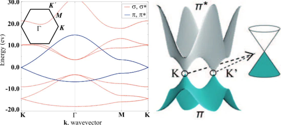
Γ K K´ M σ, σ∗ π, π∗ 30.0 20.0 10.0 0.0 -10.0 -20.0 K Γ M K k, wavevector Ener gy (ev)
Figure 2.4: Graphene band structure along the high symmetry points of the reciprocal lattice (right panel), 3D structure of the π orbitals with a linear energy dispersion near the Fermi level in the inset.
The hexagonal elementary cell of graphene contains two carbon atoms. The corresponding Brillouin zone in the reciprocal lattice has a hexagonal structure as well, however it is rotated by 90◦ with respect to the elementary
cell in the real space. The Brillouin zone contains three points of high sym-metry designated as K, M and Γ. Fig. 2.4 shows the band structure of the graphene along high symmetry points (b) and structure of only π orbitals in the first Brillouin zone computed for the reciprocal effect of three nearest neighbors (”third nearest neighbor tight-binding approximation”). The π
or-bitals are formed via binding of 2pz orbitals of two adjacent carbon atoms and
the resulting π, π∗ molecular orbitals cross at the high symmetry K–point
of the graphene Brillouin zone, exactly at the Fermi level. These orbitals in the terms of solid state physics are regarded as valence and conductance bands. Thus, graphene is a ”zero bandgap” semiconductor. The inset at the Fig. 2.4 demonstrates the linear energy dispersion of the graphene bands near the Fermi level at the K point responsible for many remarkable properties of the graphene itself [18].
The unit cell of the carbon nanotube is formed by a cylindrical surface with height T and diameter d, where T is the length of the tube translational vector. The latter is defined as the smallest graphene lattice vector perpen-dicular to Ch determining the translational period along the tube axis. It
can be calculated from chiral indexes as: T = 2m + n
gcd(2n + m, 2m + n)a1 −
2n + m
gcd(2n + m, 2m + n)a2 (2.4)
where gcd() stands for the greatest common divisor. T varies strongly with the chirality of the tube; chiral tubes often have very long unit cells.
The determination of the unit cell of the CNTs allows us to construct their Brillouin zone. The reciprocal lattice vector kz in the direction of
the tube z –axis corresponds to the transitional period T, and has a length
kz = 2π/T . As the tube is regarded as infinitely long, the wave vector kz is
continous, therefore the first Brillouin zone in the z –direction is the interval (−π/T, π/T]. In contrast to kz the wave vector k⊥along the circumference of
the tube can assume only quantized values due to the reduced dimensionality of the system. The wave function of electrons in the nanotube must have a phase shift of an integer multiple of 2π around the circumference, as all other wavelengths will vanish by interference. This implies a boundary condition on the wave vector:
k⊥,j = 2π λ = 2π |Ch| j = 2 dj (2.5)
being the number of graphene hexagons in the nanotube unit cell. Thus the first Brillouin zone of carbon nanotubes consists of nc lines parallel to
the z –axis separated by k⊥ = 2/d, Fig. 2.5. In the first approximation
the electronic band structure of a particular carbon nanotube can be found by cutting the two–dimensional band structure of graphene into nc lines of
length 2π/T and distance 2/d parallel to the direction of the tube axis Fig. 2.5. In this way, the appropriate SWNT bands are found. This approach is called zone folding and is commonly used in nanotube research. Although results obtained using this method are satisfactory in many cases, for the more precise calculation of the band structure the curvature effects and the cylindrical geometry of the nanotubes have to be taken into account.
nanotube Brillouin zones Metallic tube Semiconducting tube k = 2 d E E k y k x k y k x Bands DOS Bands DOS 6 4 8 0 2 -8 -6 -4 -2 6 4 8 0 2 -8 -6 -4 -2 Energy ( e V ) Energy (e V ) k k
Figure 2.5: From left to right: The Brillouin zone of a carbon nanotube, ”cutting lines” in the energy dispersion of the π orbitals, corresponding energy bands and density of states.
The density of states (DOS) of the SWNTs can be directly calculated from their band structure using the definition of the DOS:
DOS ∝ (dEj dk )
An example of such a derivation of the DOS for metallic (upper panel) and semiconducting (lower panel) cases are depicted on Fig. 2.5. It shows that at certain energy values the density of states exhibits sharp peaks called van Hove singularities (vHs). These maxima occur when the energy disper-sion relation has a infinitesimal upward gradient as function of k, i.e. for each extremum of the energy. These singularities are characteristic for 1– dimensional systems and combined with the peculiar properties of SWNTs give rise to several interesting phenomena. One of them is the unusual ab-sorption spectrum of these materials with many well resolved narrow peaks resulting from different chirality species. Due to the very small momentum of the absorbed photon compared to the line separation k⊥ = 2/d of the
SWNTs’ Brillouin zone, the allowed transitions are only those within the same Brillouin zone line or so–called vertical transitions. In other words the electron from any van Hove singularity below EF can be excited only to the
band which is its mirror image with respect to the Fermi level in the en-ergy band (or DOS) diagram. This transitions are usually called E11(or A), E22(B), . . . , Eii transitions and are shown in Fig 2.6.
∆k = 0 is not the only selection rule for the optical transitions in the nanotubes. One of the noteworthy properties of the electronic transitions which also arises from the reduced dimensionality is their strong dependance on the relative polarization of the electric–field vector to the nanotube axis. Depolarization or antenna effect takes place which implies that carrier exci-tations are possible only with the field component parallel to the tube axis. For external fields applied in other directions charges are induced on the cylinder walls. The resulting polarization vector opposes the external field and reduces the electric field.
As mentioned above, a very interesting electronic property of the carbon nanotubes is their either semiconducting or metallic nature. As depicted in Fig 2.6 two typical structures are possible for the energy bands. When the cutting line of the Brillouin zone goes trough K point the density of states has a finite value at the Fermi level due to the respective linear energy
Ener
gy
(e
v
)
semiconducting tube metallic tube
Figure 2.6: Energy dispersion and density of states of semiconducting (left) versus metallic (right) tubes, near the Fermi level. For metallic nanotubes because their Brillouin zone the K point of the graphene reciprocal lattice a finite density of states exists at Fermi level.
bands. These nanotubes have metallic characteristics. In all other cases a bandgap opens between the first two vHs and the nanotubes are semiconduct-ing. Strictly speaking, a tiny gap exists also for the non–armchair metallic tubes because of the curvature effects[19, 20]. Nevertheless, for most prac-tical purposes and for most experimentally observed carbon nanotube sizes this gap would be so small that, all the n − m = 3j tubes can be consid-ered as metallic at room temperature. From geometrical considerations it is obvious that one–third of all possible SWNT structures will be metals while two–third will be semiconductors.
The size of the gap depends on the diameter of the SWNTs as result of the spatial confinement of electrons in the radial direction. However, the dependence is not simply inversely proportional to the diameter as in the case of e.g. quantum dots, but depends also on the chirality of a certain tube in an elegant manner:
E
S 11E
S 22E
M 11E
S 33Figure 2.7: The Kataura plot showing the dependence of the electronic transitions in nanotubes on their diameters. The separation of the van Hove singularities scales with the inverse diameter. Black points corre-spond to semiconducting nanotubes and red points to the metallic ones.
E11= 2γ0a0d−1+ (−1)υ
t11cos 3θ
d2 (2.7)
where γ0 and t11 are free parameters related to the onsite energy and
to the hopping integrals, respectively, d is the nanotube diameter, and θ is the nanotube chiral angle. Fig. 2.7 shows the computed transition energies
Eii of semiconducting and metallic SWNTs for different n,m pairs for the
diameter range up to 3 nm. The subscript indexes designate the appropriate pair of van Hove singularities, while the superscript indexes ”S” and ”M” refer in each case to metallic or semiconducting SWNTs. This kind of the representation is the so-called Kataura plot [17].
2.3
Optical Properties
2.3.1
Photoluminescence
As most CNT species are semiconducting it was commonly expected that these materials should be luminescent. It was anticipated that the carriers excited to the higher vHs will relax to the band edge of the first singularity followed by a radiative recombination to the valence band. However lumi-nescence from carbon nanotubes was not observed for many years after their discovery in early 90s. The main obstacle here is apparently the low intrinsic quantum efficiency of the system. Another very important reason that hin-ders the tube to radiate is their tendency to form small bundles and ropes in most of the samples. The van der Waals forces between individual tubes can be as strong as 500 eV/µm tube–to–tube contact and favor the aggre-gation of the tubes into bundles. The exact mechanism which quenches the radiative recombination in the bundles is still a matter of debate. Suppos-edly, the energy transfer [21, 22] from the excitations in the semiconducting tubes to the metallic ones and their subsequent radiationless relaxation is one of the main contributing reasons. Other speculations suggest alterations in the band structure of the individual tube due to the inter–tube interactions which might create sites with non–zero density of states near the Fermi level along the nanotube. Some of the factors influencing non–radiative relaxation channels in CNTs will be discussed later in this work.
In order to prevent the bundling process a procedure of coating the in-dividual tubes with surfactant molecules was successfully implemented by Weisman and coworkers [23]. The surfactant molecules (sodium dodecyl sul-fate (SDS)) used in this pioneering work and also in subsequent improved methods have hydrophobic head that aggregates with the nanotube sidewalls and hydrophilic long tails. Ultrasonic agitation of an aqueous dispersion of raw single–walled carbon nanotubes and surfactant material and subsequent centrifugation to remove tube bundles, ropes, and residual catalyst resulted in individual nanotubes, each encased in a cylindrical micelle. Free from the
per-turbation of surrounding tubes and surfaces, the tubes in these suspensions show much better resolved optical absorption spectra. Most importantly, the one-dimensional direct band gap semiconducting tubes in these samples are now found to fluoresce brightly in the 800– to 1600–nm wavelength range of the near infrared. Later analysis of the discrete peaks in photoexcitation emission maps [24] and combined Raman and photoluminescence measure-ments from single carbon nanotubes [25] allowed unambiguous assignment of the emission peaks to certain tube chiralities.
a
b
Figure 2.8: Photoluminescence from carbon nanotubes. (a) the emission and absorption spectra of the aqueous solution of surfactant coated nan-otubes, with the cross section of the carbon nanotube model encapsulated into a SDS micelle in the inset. Well resolved peaks belonging to different nanotube charities are present in both spectra. (b) photoluminescence in-tensity as a function of emission and excitation wavelengths, from [23, 24].
Fig. 2.8 shows the well resolved peaks in the absorption and emission spectra of the micelle encapsulated SWNTs aqueous solution (a) and pho-toluminescence excitation map of the material (b). In the contour plot the fluorescence intensity versus excitation and emission wavelengths is depicted. Each feature in the region marked by a white ovale corresponds to the E11
emission of a certain (n,m) species after their excitation to the second van Hove singularity of the conduction band. Similar results were reported for in-dividual nanotubes suspended in air, free of substrate interaction [26, 27, 28].
2.3.2
Excitons
The electronic structure of SWNTs presented above does not take into ac-count the electron–electron interactions but assumes free non–interacting carriers. However, strong confinement of electrons in the 1–dimensional ge-ometry suggests that these interaction can significantly influence the band structure. Indeed, early theoretical calculations predicted that because of strong Coulomb interaction the excited electron in the conduction band and the hole in the valence band will form strongly correlated entities known as excitons [29, 30, 31, 32]. Another important effect that results from Coulomb interactions is the so called band gap renormalization (BGR). Electron– electron repulsion in the stongly confined 1–D system leads to a larger energy gap compared to the free carrier picture. The net impact of these two effects results in optically active singlet excitonic states with an energy close to cal-culated values based on zone folding free carrier approximation. Moreover, in contrast to 3D or 2D materials the density of states for one dimensional structures with sharp singularities does not change significantly with the ad-dition of excitonic states. These factors made the existence of the excitons in the CNTs elusive in the early stages of carbon nanotube research.
As a result of strong Coulomb interaction strongly bound hydrogen-like excitonic states are formed below the energy of the vHs. The structure of these excitonic states determines the optical, electronic and other properties of the nanotubes. Moreover, the unique electronic structure of the graphene and SWNTs give rise to interesting features of the excitonic manifold. Two special points in the Brillouin zone the K and K’ points, emerge as a result of the unusual geometrical structure of sp2 hybridized carbon atoms. These
points are related by time-reversal symmetry [33] and therefore the conduc-tion and valence bands in the vicinity of these points constitute two sets of inequivalent bands (Fig. 2.9 a), Fig. 2.10 a)) making carbon nanotubes dif-ferent from other nano systems, which also have large excitonic effects, but do not have similar symmetry constraints. Although an optical transition occurs vertically in k space, we can consider the electron and the hole in the
electron-hole pair to be either in the same valley, or an electron to be in one valley and a hole in the other valley. The latter pair can form an excitonic state, but it never recombines radiatively because the electron and hole do not exist in the same valley; such a state is called a dark exciton Fig. 2.9 b). Differences in symmetry are important and guide electronic-structure calculations and the interpretation of experiments. Therefore, an analysis of exciton symmetries in SWNTs is needed to understand in greater detail many aspects of their optical properties.
K K K K' K' K' M M M M M M M M Γ K K
K
K'
K' K' K K' K' Ka
b
h eFigure 2.9: a)Brillouin zone of the (6,5) nanotubes showing to inequivalent valley near K and K’ points (adopted from [33]). Electron (filled cycle) and the hole (empty cycle) are depicted on the cutting lines in the vicinity of K and K’ points, respectively . b) the four excitonic states formed as a result of mixing of two bands near the K and K’ points.
Because the exciton wave function is localized in real space by a Coulomb interaction, the wave vector of an electron (ke) or a hole (kh) is not a good
quantum number any more, and thus the exciton wave function Ψn for the
n-th exciton energy Ωn is given by a linear combination of Bloch functions
at many ke and kh wave vectors.
Ψ(~ke, ~kh) =
X
v,c
Avcφc(~ke)φ∗v(~kh), (2.8)
Then the Fourier transformation of the localized exciton (e.g. a Gaussian wave packet) wave function will obviously result in a localized wave function also in k–space and thus we can define the central position of the latter as a wave vectors of the of the electron and the hole in the bound exciton. For the theoretical determination of the coefficients Avc and to obtain the mixing of
different wave vectors by the Coulomb interaction it is necessary to solve a Bethe–Salpeter equation which incorporates many-body effects and describes the coupling between electrons and holes.
X ke,kh ((E(~ke) − E(~kh))δ~k0 e~keδ~k0h~kh+ K(~k 0 e~kh0, ~ke~kh))Ψn(~ke~kh) = ΩnΨn(~ke0~kh0), (2.9) where E(~ke) and E(~kh) are the quasi-electron and quasi-hole energies,
re-spectively and are the sum of the single-particle energy and the self-energy. The self-energy encodes the exchange-correlation potential an excited quasi– particle feels due to the surrounding electronic medium, and it is nonlocal and energy dependent. Here quasi-particle means that we add a Coulomb interaction to the one-particle energy and that the particle has a finite life-time. Equation 2.9 represents simultaneous equations for many k0
e and kh0
points. The K(~k0
e~kh0, ~ke~kh)is the mixing term which takes into account the
direct and exchange interactions of spin-singlet and spin–triplet states. Although by solving Bethe–Salpeter equation it is possible to calculate the exact excitonic manifold of the system [30, 31] some important optical properties like the above mentioned availability of the excitonic state from the ground state can be obtained only from symmetry considerations [34]. For this purpose the effective mass and envelope function approximation (EMA) [35] can be used and the final excitonic wave function’s symmetry can be directly related to the symmetry of the conduction and valence states where the electron and the hole forming the exciton originate from. It is important to note that for the use of the approximation the contributions from only 1st (n-th) van Hove singularity states can be used which is justified given the large energy separations of the singularities. Thus the approximate
wave function ψEM A(~r e, ~rh) = X v,c 0B vcφc(~re)φ∗v(~rh)Fν(ze− zh) (2.10)
will have the same symmetry as the real wave function. Here the prime in the summation indicates that only states from the given singularity are included. The ”hydrogenic” envelope function Fν(ze− zh) provides the
local-ization of the exciton along the principal z axis of the nanotube and ν labels the levels in the 1D hydrogen–like series. The use of this envelope function is dictated from general physical considerations for the ordering in which the different exciton states appear. Finally, to evaluate the symmetry of the excitonic state its irreducible representation D(ψEM A) should be examined.
The D(ψEM A) is simply related to the product of the respective irreducible
representations of the conduction state D(φc), valence state D(φv) and the
envelope function D(Fν)
D(ψEM A) = D(φc) ⊗ D(φv) ⊗ D(Fν) (2.11)
We can now apply the Eq. 2.11 to study the symmetry related properties of the excitons in nanotubes. Here we consider only E11 transitions of the
most general case of the chiral nanotubes as they were subject of the exper-imental studies of the current work. The similar discussion for the achiral (zigzag and armchair) nanotubes can be found in the original work of Barros
et al. [34].
Fig. 2.10 a) shows the two inequivalent bands in the vicinity of K and K’ points of the nanotube’s Brillouin zone. As mentioned above these two bands are related by time-reversal symmetry and have band extrema at ± k points. The symmetry of these bands in the commonly used molecular sym-metry notation1 [37] are E
µ(k0) and E−µ(−k0). Here E stands for the doubly
degenerate representation and µ is the quasiangular momentum quantum
1For the description of the symmetries of the nanotubes the so called ”line group”
notations were also introduced which provide somewhat more convenient but equivalent labeling. [36]
a
b
Figure 2.10: Forming of excitonic states in a chiral nanotube [34]. (a) The inequivalent pair electron and hole bands in a free carrier picture, (b) corresponding four excitonic bands with different symmetries. The electron hole and exciton states at the band edges are indicated by a solid circle and labeled according to their irreducible representation.
number associated with the cutting lines of the Brillouin zone. Thus for the lowest ”hydrogen level” of the envelope function ν = 0 with the absolutely symmetric A1(0) representation we have
(Eµ(k0) − E−µ(−k0)) ⊗ (E−µ(−k0− Eµ(k0)) ⊗ A1(0)
= A1(0) + A2(0) + Eµ0(k0) + E−µ0(−k0) (2.12)
where k’ and µ’ are the exciton linear momenta and quasiangular mo-menta respectively. Here for A1 and A2 symmetries A stands for the
sym-metrical rotation around the principal axis with odd and even parity respec-tively for subscripts 1 and 2. The resulting four lowest set of excitonic bands is shown in Fig. 2.10 b). The excitonic bands that have an energetic mini-mum at the Γ point result from electron and hole states from different bands (near K and K’ points). As the ground state of the nanotube has a totally symmetric A1 representation only one of these two excitonic states fulfills
with the nanotube axis. This is a consequence of the fact the interaction between the light polarized along the principal axis and the electric dipole moment in the nanotube transforms as the A2 representation for the chiral
nanotubes [38]. Thus, only the product of A2 state with the symmetry of the
interaction equals to the ground state’s symmetry and the other state is a optically inactive dark state. The other two states formed by the same K and K’ bands will be dark as well because they do not match the selection rules for both symmetry and momentum (they have non–zero momenta). Other values of the envelope function ν (odd and even) will leave the decomposition in the Eq. 2.12 unchanged, hence, there will be one and only one optically active excitonic state per each ν.
The similar set of excitonic bands exists also for triplet excitons which have lower energies compared to singlet states [39, 40, 41]. The obvious difference is that triplets are non–emissive due to the spin selection rule. Thus only from symmetry considerations it becomes obvious that not all excitonic states are emissive. However if the ideal structure of the nanotube is modified e.g. by defect introduction, the discussed selection rules can be relaxed because of the change in the symmetry of the structure [39]. In this case the exciton state can be formed by mixing of states with different parity and multiplicity depending on the nature of the introduced defect. In Chapter 5 we will show for the first time the experimental realization of this effect. By intense pulsed laser excitation and by interaction of metal atoms with the individual nanotube we show that singlet A1 symmetry and triplet
states can be ”brightened” i.e. turned into emissive.
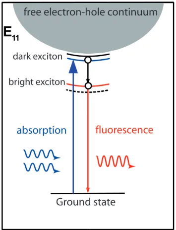
The existence of strongly bound excitons was experimentally observed us-ing the described peculiarities of their electronic states (Fig. 2.11). Namely, the states inaccessible from the ground state with a one photon absorption can be accessible if two photons are absorbed simultaneously. If this state has a higher energy (ν > 0) than the lowest optically active state (ν = 0) it can decay non–radiatively to the latter state and emit a photoluminescence photon. Thus the difference between the energy of the two absorbed photons
and the emitted photon will manifest the excitonic nature of the excited state and will determine the binding energy of the excitons.
free electron-hole continuum
fluorescence
absorption
dark exciton
bright exciton
Ground state
Figure 2.11: Schematics showing the experimatal approach to identify the nature of the excited states in carbon nanotubes. The two–photon absorbtion into the dark excitonic state is followed by its radiationless relaxation to bright state and subsequent fluorescence. The difference in the energy of the absorbed and emitted photons determines the biding energy of the exiton.
This experimental approach was successfully implemented by two groups [8, 42] and exciton binding energies (Eb) up to 1 eV have been determined.
Thus, the exciton binding energy constitutes a substantial fraction of the gap energy. For comparison the exciton binding energies in bulk semiconductors typically lie in the range of several meV and represent a slight correction to the band gap [43].
These significant binding energies suggest that the excitons in SWNTs should be more strongly localized than their weakly bound bulk counter-parts. Indeed, the wavefunction of the excitons was found to be fully delo-calized along the circumference of the nanotube and strongly lodelo-calized along the nanotube axis, with resulting exciton Bohr radius corresponding to the envelope function defined in Eq. 2.10 of ∼3nm [8, 44]. Thus, the size of the exciton is comparable and even larger than the diameter of the nanotube and as a result the effect of the lattice potential can be incorporated into the effective masses of the electron and hole as is usually done for the so called Wannier–Mott excitons.
The size of the excitons in the nanotubes also implies that their binding energy will be very sensitive to the environment. The Coulombic coupling between the electron and hole forming the 1D exciton, as in the case of bulk excitons, depends on dielectric screening. In bulk excitons the binding energy is proportional to 1/ε2, where ε is the dielectric function of the material. In
nanotubes, when the exciton size is larger than the tube diameter, most of the electric-field lines between charges penetrate the surrounding medium and this makes the exciton binding energy (as well as the bandgap) a function of the dielectric constant of the surrounding environment. Perebeinos et al. [31] gave the following expression for the dependence Eb on CNT diameter (d),
chirality through the effective mass (m∗) and dielectric constant (ε):
Eb = Cdα−2m∗α−1εα (2.13)
where α = 1.4. Hence, the poor screening in the vacuum or dielec-tric environment outside of the nanotube allow for significant binding ener-gies of 0.4-1.0 eV characteristic for Frenkel type excitons. This dual nature (Wannier–Mott and Frenkel type) of the excitons is a unique feature of car-bon nanotubes. The excitonic nature of the excitation was shown even in metallic nanotubes with combination of Rayleigh scattering and absorption spectroscopy [45]. Normally, one does not find bound excitons in bulk metal-lic systems because the long-range part of the electronhole interaction is
screened out completely by the available carriers. However, the reduced di-mensionality leads to the incomplete screening of Coulomb interactions and exciton formation.
Thus, in carbon nanotubes the excited state oscillator strength is almost completely transferred from the free carrier band edge to the excitonic man-ifold. The former still exists with a far smaller weight and does not play a major role [46]. The described excitonic structure of the carbon nanotubes has a very important impact on optical, electronic and other properties of this material. Naturally, it influences also the dynamics of the excited state discussed in present work.
2.4
Excited State Dynamics
Recent rapid advances in synthesis of high quality, low cost nanotube materi-als opened perspectives for new applications in different promising fields deal-ing with optoelectronic properties of CNTs, e.g. ultracompact and narrow-band emitters and detectors. Knowledge of excited state dynamics of these systems is absolutely crucial for achieving desired goals as it probes the funda-mental properties of the CNTs like electron-photon/phonon coupling, exact electronic/excitonic structure, nature of the various defect states, impact of the environment on the electronic processes and many other interesting and important characteristics. In this work these questions are addressed by in-vestigating the exciton recombination lifetimes of single carbon nanotubes at room temperature.
In any electronic system after absorption of a photon with an appropriate energy matching the transition resonance of its electron, an excitation from the ground state to higher energy electronic states occurs. The characteristic time needed for the electron to return to the ground state is called lifetime of the excited state. Decay channels influencing the effective lifetime can be divided in two major groups: radiative and non–radiative. Radiative relaxation is associated with the emission of a photon whereas non–radiative
relaxation can have various pathways such as coupling to phonons, energy transfer to the environment, quenching by other molecules or by intrinsic defects. A useful measure for this output is the quantum yield defined as
η = γr
γr+ γnr
(2.14) where γr and γnr are radiative and nonradiative decay rates, respectively
(inverse of lifetime τ ) .
Figure 2.12: Schematic representation of the commonly accepted picture of the excited state’s relaxation channels in the CNTs. The exciton pumped into its first excited manifold by an external stimulus relaxes to the ground state predominantly via non–radiative relaxation channels.
The radiative lifetime of the system is given only by the oscillator strength of the specific excited state. For the SWNTs theoretical calculations [47, 39] predict this parameter to be in the range of ∼ 10ns at room temperature. On the other hand all the measurements of the ground state recovery lifetime using different methods, samples and environments give us lifetimes that
are faster by several orders of magnitude and very low quantum yields were measured in the range of 10−3. This fact indicates that the total decay rate
γ = γr+ γnr is dominated mainly by the non–radiative decay channels. One
of the main goals of this work is to discuss the possible mechanisms of the non–radiative relaxations of excitons in the SWNTs.
Many measurements on excited state dynamics have been reported during the last several years, for various samples of SWNTs using different methods. Although these findings step by step bring us closer to the full understanding of the principal properties of the problem, there is a large variety of differ-ent observations often contradicting each other. This concerns mainly the timescale of the ground state recovery ranging from sub–picosecond dynam-ics to several hundreds of picoseconds, the time dependence of the exciton recombination and the exact structure of exciton manifold’s electronic states. Apparently, this discrepancies are due to differences in the sample prepara-tion and processing as well as to different measuring methods. As many of this experiments were done on ensemble samples, the averaging over individ-ual features of single nanotubes like defect concentration, length, coupling to the environment, bundling also contributes heavily in complicated and some-times controversial interpretations of the data. Thus, in this work we tried to use an approach that would simplify the matter and reduce the number of unknown parameters by investigating individual SWNTs and by using rel-atively straightforward Time Correlated Single Photon Counting (TCSPC) technique for measuring time resolved photoluminescence. Previously this approach was used to measure SWNTs exciton decay lifetimes at low tem-perature [9] and quite a big variation of recombination lifetime for different tubes (20–180ps) was detected. At room temperatures similar experiments might seem to be challenging as the PL intensity is reduced by a factor of
∼ 5 and the decay times are also decreased dramatically [9, 48, 49]. However,
the results shown here indicate that a well optimized confocal laser scanning microscope setup is capable for such investigations and we can benefit largely from advantages of the ambient conditions. Moreover, from the application
point of view room temperature measurements are even more valuable as most of the devices are supposed to work in these conditions.
First studies on the excited state dynamics of SWNTs were done mainly using the so called ”pump–probe” techniques. In these experiments two spa-tially overlapped beams from pulsed lasers are used. The first beam excites the system from its grounds state and the second beam probes the evolution of the excited state. The measured signal here is the enhanced or reduced transmission of the probe beam through the sample respectively due to ei-ther stimulated emission and photobleaching or excitation of the system to even higher electronic states. Thus, by varying the time delay between the two pulses one can investigate dynamic electronic processes of the system. Though this technique has a major advantage, that is the temporal resolu-tion of the experiment is limited only by the laser pulse duraresolu-tion and not by the response time of the detection electronics, very often there are compli-cations in the interpretation of the data caused by different types of signals (positive and negative) and overlapping contributions in different spectral regions from various nanotube species. Besides this, the powers usually used in these experiments are relatively high in order to be able to detect the small variations in the transmission. High power excitations however, are shown to cause additional non–linear processes in the excited state dynamics like Auger recombination or exciton–exciton annihilation [50, 51, 52] which further complicate the matter substantially.
Nevertheless, valuable information have been obtained using this method for semiconducting SWNTs excited to their first excitonic state. They were shown to exhibit a very fast recovery to the ground state with time constant of ∼ 1 ps, attributed to nonradiative decay [53, 54, 55, 56]. By correlating the photoinduced absorption signal corresponding to the difference of the first and second excitonic bands’ energies with the photobleaching from the first excitonic band Manzoni et. al. [57] determined the time constant of
∼ 40f s for the intersubband exciton relaxation. The availability of
well as chirality enriched materials [58], made it possible to improve the un-derstanding of these experiments. The detection of signals indicating the transitions of excited electrons to other non–emitting states (dark excitons or non–emitting trap states), made it closer to the full understanding of the dynamical properties of the system [59], [60].
On the other hand, the discovery of the bandgap photoluminescence from surfactant coated semiconducting carbon nanotubes [23, 24, 25] enabled the direct measurement of the decay rate of the PL. Early measurements on suspension of isolated SWNTs using Kerr gating [61] technique showed bi-exponential decay with a fast component in the order of ∼ 7ps attributed to intrinsic non–radiative relaxation channels. In that work authors suggested that given the extremely low fluorescence quantum efficiency, η, of carbon nanotubes (∼ 10−4) the intrinsic radiative lifetime γ
r can be estimated to be
as long as ∼ 100ns.
Several other measurements of time-resolved fluorescence reported some-what longer lifetimes with mono- [62, 63, 48], bi- [64] and multiexponential decay dynamics [49]. The short lived components within 10–60 ps is usu-ally believed to be due to coupling to either extrinsic relaxation channels like radiationless energy transfer to metallic tubes in the small residual bun-dles or to intrinsic non emissive states. The observed long lived components in some experiments ranging from several hundreds of picoseconds to sev-eral nanoseconds are attributed to the real intrinsic lifetime of individual SWNTs.
Experimental
3.1
Confocal Microscopy of Single Carbon
Nan-otubes
The measurement of the excited state dynamics of the single carbon nan-otubes consists of two main parts. First, the individual nannan-otubes are iden-tified on the substrate by confocal microscopy and afterwards the exciton recombination lifetime is measured using Time Correlated Single Photon Counting (TCSPC) technique.
The concept of confocal microscopy, depicted in the Fig. 3.1 is to excite the material resting on the substrate by a tightly focused diffraction lim-ited spot of the excitation beam from the light source (typically a single mode laser source) and then to detect the locally generated optical signal by guiding it through a pinhole [65]. The latter is done in order to avoid the background originating not from the excitation area. The small detection area of the detector can also act as a spatial filter, i.e pinhole. The measured optical response of the system can be different types of light–matter inter-actions, such as elastic or Raman scattering, fluorescence, higher–harmonic generation etc. To generate an image of the optical response from the sam-ple either the laser beam or the samsam-ple itself has to be raster scanned. The availability of translators based on piezoelectric actuators made it possible
objective focusing lens detector detection plane sample pinhole laser beamsplitter
Figure 3.1: Schematic of the confocal microscopy. Only the signal em-anating from the focal point of the objective can reach the detector(red solid line). Light emanating from other spots(blue dashed line) is blocked by the pinhole.
to scan areas with nanometer precision.
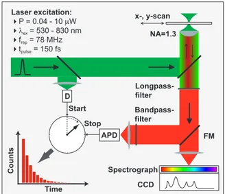
The confocal microscopy setup is depicted on Fig. 3.2. The excitation source is a Coherent Mira 900 Ti:Sapphire laser. It is pumped by a Coherent Verdi diode–pumped solid state laser operating at 532nm wavelength with 5W output power. The Ti:Sapphire laser can operate either in continuous wave (CW) or in pulsed (mode–locked, ML) regime with pulse duration of 150fs and repetition rate 78 MHz. The operating wavelength can be tuned from 750nm to 900nm depending on the experimental objectives. The typical output power is in the range of 50mW, though for our purposes beams with far less intensities are used in the range of 1µW–200µW. The laser line filter (LLF) with a narrow spectral transmission matching the laser wavelength is located in the beam–path to suppress the fluorescence of the Ti:Sapphire crystal. The set of neutral density (ND) filters reduce the intensity of the
M3 M2 M1 Sample Scanstage Objective Retroreflector M4 Flip Mirror Monochromator Beam-splitter LP Filter BP Filter L1 L2 M5 LL Filter ND Filters set Pump laser Ti :Sp p h ir e pulsed laser
Figure 3.2: The basic elements of the experimental setup. Excitation is provided by a pulsed tunable laser, confocal detection principle is used to measure PL spectra(spectrometer) and transients(APD) from individual nanotubes.
laser beam to obtain powers required for a given experiment. Next, the beam is guided into the inverted microscope (Nikon Eclipse TE2000 E) with a set of mirrors (M1, M2, M3). To split the excitation path and the detection path into two separate arms a beam splitter is introduced with a transmittance to reflection ratio of 70/30. Afterwards, the beam is focused onto the sam-ple by an oil immersion objective (Nikon Plan Fluor S) with 1.3 numerical aperture (NA). The high NA objective allows us to have an excitation spot size ∆x ≈ 0.61λ/NA as small as half the wavelength of the excitation beam and therefore high lateral resolution of optical signals. Collection angles
ex-ceeding the angle of total internal reflection reached for NA > 1 maximize the detection efficiency and are also very crucial for the observation of weak signals emanating from nanoscale emitters as in the case of single carbon nanotubes. The sample, typically a microscope cover slip spin coated with the CNT solution, is then raster scanned by a XY piezo scan stage (Physik Instrumente, P-517.2CL) and at each position the optical signal from the sample is collected in epi-illumination configuration. A retroreflector is used to guide the detection path either to the eye piece or the side port of the inverted microscope.
In the detection path the first element usually is the one that should sup-press the excitation background. As we work mainly with spectrally shifted signals with respect to the excitation, e.g. photoluminescence, a long–pass (LP) interference filter is used to block the laser. With the help of a flip mirror the signal can be guided either to the avalanche photo diode (APD)(MPD, PDM 5CTC) or to the spectrometer depending on the measurement goals. Alternately a 50/50 beamsplitter can be used instead of a flip mirror if the simultaneous detection of spectrum and the PL transient (vide infra) is de-sired. As usually the imaging is done with an APD the signal is guided through a lens to focus it onto the small detection area of the APD of 25µm. As previously mentioned the pinhole is not needed in this case and confocal detection is secured by the small size of the detector. Typical acquisition times per pixel for APD imaging are in order of 20–60ms depending on ex-citation power. If the detection of the PL signal from a specific chirality nanotube is desired then a narrow band–pass (BP) filter corresponding to the particular chirality emission energy is inserted in front of the APD. Be-sides the imaging the photodiode is used also to measure the time resolved photoluminescence from single carbon nanotubes as will be described in the next section. In this last case the presence of the bandpass filter, matching the emission wavelength of the tube, in front of the APD is obligatory as the residual fundamental photons not suppressed by the LP filter can bring misleading results.
500 600 700 800 900 1000 0.0 0.2 0.4 0.6 0.8 1.0 Q u a n tu m e ff ic ie n cy Wavelength, nm Grating CCD Total APD
Figure 3.3: The quantum efficiency curves for the detectors used in the current work. a) the QE of the CCD camera and the spectrometer grating, b) the QE of the APD. The curves show typical behavior of Si based detectors that become ”blind” for wavelengths longer than ∼1000nm.
The spectra of the SWNTs are measured by flipping up the mirror and guiding the signal to the spectrometer (Andor Technology, Shamrock 303i). An additional lens is situated in front of the spectrometer to focus the light through the entrance slit. The size of the slit can be varied and can be reduced down to 10µm thus, if needed, it can act as a pinhole. Inside the spectrometer the signal is dispersed by a dispersion grating which operates in Czerny-Turner configuration. The dispersed spectrum is then recorded by charged coupled device (CCD, Andor IDUS OE DU420) camera, thermoelectrically cooled to −60◦C. The typical integration times for obtaining a spectrum
from a single nanotube is in the range of 2–30 seconds depending on the emission rate. The spectroscopic imaging of the sample, i.e. recording the spectrum of the sample at each pixel in principle is also possible, however it requires much longer acquisition times given the slow readout speed of the CCD.
The quantum efficiencies (QE) of the detectors used in this work are depicted in Fig 3.3. The working materials of these detectors are based on Si, which has a band gap 1.12 eV at room temperature, therefore their QE decreases drastically at wavelengths longer than ∼ 1000nm. This limits our studies on the photoluminescence of the SWNTs to those which have a band
gap larger than 1000nm i.e. diameter smaller than ∼ 0.8nm according to the Kataura plot 2.7. However, the CoMoCat nanotubes used in this work have a quite narrow diameter distribution peaking at about 0,8nm [66] and based on the comparison of the density of the nanotubes on the microscope cover slips determined from Atomic Force Microscopy (AFM) measurements and optical imaging (vide infra) we conclude that most of the nanotubes present in our samples emit in the detection range of our system.
The total detection efficiency of the system can be estimated from the absorption cross section and the quantum yield of the emitter and the actual count rate detected at the detector. The quantum yield of the SWNTs is in the range of 10−3 [9] and absorption cross section is ∼ 10−18cm2/atom [67,
68]. The typical count rate detected at the APD from the PL of the nanotube in the focus of the 1014pulse−1cm−1 intensity excitation is ∼ 1000Hz. Taking
into account the repetition rate of the Ti:Sapphire laser of 78 MHz we get an estimation of the overall detection efficiency of the setup of ∼ 10−3.
3.2
Time Correlated Single Photon Counting
Time-correlated single photon counting (TCSPC) is a sensitive technique for recording low-level light signals with picosecond resolution and extremely high precision [69]. Photon counting techniques consider the detector signal a random sequence of pulses corresponding to the detection of the individual photons. Therefore, the detector signal is a random sequence of single-photon pulses rather than a continuous waveform. The light intensity is represented by the density of the pulses, not by their amplitude. Obviously, the intensity of the light signal is obtained best by counting the pulses in subsequent time channels. A unique feature of photon counting results from the fact that the arrival time of a photon pulse can be determined with high precision. The bandwidth of a photon counting experiment is limited only by the transit time spread of the pulses in the detector, not by the width of the pulses.
de-Original Waveform Detector Period 1 Period 5 Period 6 Period 7 Period 8 Period 9 Period 10 Period N Period 2 Period 3 Period 4 Result after Photons Time Signal: many (Distribution of photon probability)
Figure 3.4: The principle of the TCSPC method. The histogram of the detected counts is constructed based on their arrival time. The measure-ments over many excitation cycles result in a time–resolved signal curve
tection of single photons of a periodic light signal, the measurement of the detection times, and the reconstruction of the waveform from the individual time measurements. TCSPC makes use of the fact that for low-level, high-repetition rate signals, like single SWNT flourescence, the light intensity is usually low enough that the probability to detect more than one photon per one laser excitation pulse is negligible. The detector signal consists of a train of randomly distributed pulses corresponding to the detection of the individ-ual photons. There are many signal periods without photons, other signal periods contain one photon pulse. This situation is depicted in Fig. 3.4.
When a fluorescence photon is detected, the arrival time of the corre-sponding detector pulse in the signal period is measured. The events are collected in a memory by adding a 1 in a memory location with an address proportional to the detection time. After many signal periods a large number of photons has been detected, and the distribution of the photons over the
NA=1.3 CCD Spectrograph Laser excitation: 4P = 0.04 - 10 µW 4λex = 530 - 830 nm 4frep = 78 MHz 4tpulse = 150 fs APD x-, y-scan FM D Start Stop Bandpass-filter Longpass-filter Counts Time
Figure 3.5: The schematics of the TCSPC experiment. The delay time between a laser excitation pulse (start pulse) and the detected PL photon (stop puls) is determined by a TCSPC acquisition card.
time in the signal period builds up. The result represents the waveform of the optical pulse. In other words the generated laser pulse starts the clock and afterwards the PL photon created by the same pulse stops the clock and the measured waveform shows the characteristic delay between the excitation and the emission. The latter is governed by the dynamical properties of the excited state of the sample.
To measure the signal period the exact excitation time of the signal should be known. This is provided by connecting the output of the detector in-side the laser which monitors the pulse generation directly to the TCSPC card(SPC-140). Another input of the card is connected to the APD to de-tect the ’stop’ pulse from PL signal. This configuration is schematically represented in the Fig. 3.5. Typical accusation times for a PL transient are in the range of 30-500 seconds.
Exciton Decay Dynamics in
Individual Carbon Nanotubes
at Room Temperature
4.1
General Procedure for Exciton Lifetime
Measurements
In this chapter exciton lifetimes of individual CNTs are measured using the TCSPC method combined with confocal microscopy as described in the ex-perimental chapter. Here, for the first time, the results on time–resolved photoluminescence (PL) of individual SWNTs at room temperature are pre-sented. The exciton recombination follows strictly monoexponential decay over four orders of magnitude with time constants varying from tube to tube in the range of ∼ 1 to 40ps for the same chirality tubes. The impact of parameters expected to influence the exciton decay, like nanotube length, environment and defect concentration on the photoexcitation relaxation pro-cess is discussed.
Samples are prepared by spin coating an aqueous solution of surfactant coated CoMoCat SWNTs [70, 71, 72] on the microscope glass cover slip.
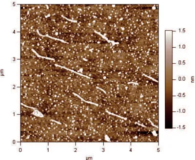
Di-luted solutions are used in order to obtain samples with individual nanotubes and to prevent bundling. The atomic force microscopy (AFM) measurements of the samples show well dispersed, isolated, extended structures (Fig. 4.1). The height of these structures ∼2nm is somewhat bigger than expected for single tubes ∼0.8nm. This is due to the surfactant layers covering the tubes. The residual surfactant can also be seen in the AFM image in a form of small dots with similar height. Almost parallel orientation of the tubes is a result of the spin coating procedure.
Figure 4.1: Typical AFM image of the sample containing micelle en-capsulated nanotubes. Well separated, elongated features are individual SWNTs. The height of the features exceeds single nanotube diameter due to the layer of the surfactant covering the tubes.
Nanotubes are imaged by raster scanning the sample by means of piezo XY scanner and detecting the optical signal from individual tubes with the APD [73]. As the aim of our studies is to investigate the time resolved radiative recombination of the excitons in CNTs, the typical signal detected during the scanning process is the fluorescence from single SWNTs. The detection of inelastically scattered Raman photons to identify the nanotubes


![Figure 2.10: Forming of excitonic states in a chiral nanotube [34]. (a) The inequivalent pair electron and hole bands in a free carrier picture, (b) corresponding four excitonic bands with different symmetries](https://thumb-eu.123doks.com/thumbv2/123dokorg/7347203.92676/28.892.170.711.199.438/excitonic-nanotube-inequivalent-electron-corresponding-excitonic-different-symmetries.webp)