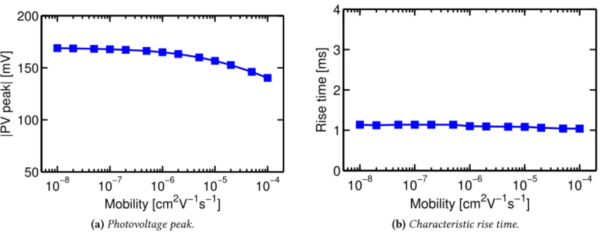
Politecnico di Milano Department of Mathematics
Doctoral Programme in
Mathematical Models and Methods in Engineering
Bio-Polymer Interfaces for
Optical Cellular Stimulation:
a Computational Modeling Approach
Doctoral Dissertation of:
Matteo Porro
Supervisor:
Prof. Riccardo Sacco
Co-advisors:
Prof. Guglielmo Lanzani Dr. Maria Rosa Antognazza
Tutor:
Prof. Riccardo Sacco
The Chair of the Doctoral Program:
Prof. Roberto Lucchetti
Abstract
The present thesis concerns with the investigation and the mathematical description of the physical processes underlying the behavior of a particular bio-polymer interface device for optical cellular stimulation. Such device is made of a thin slab of P3HT, a photoactive semiconducting conjugated polymer, sandwiched between a cell and a transparent electrode, the whole system being immersed in a physiological solution to allow cell survival during experiments.
Despite the fact that measured cell membrane current and potential clearly demon-strate that a significant electrical cellular activity is elicited by light mediated stimu-lation due to absorption by the polymer, the physical processes driving the induced cellular response are still not fully understood. To fill the gap of a lack of a consistent understanding and of a quantitative description of the device working principles, the present thesis proceeds according to a three-step procedure.
In the first step, a systematic classification of performed measurement is carried out, distinguishing between measurements with the sole polymer part of the device and measurements including the cell. In the second step, based on a thorough scrutiny of the two classes of experimental data, an identification of the principal physical phenomena is operated, concluding that electrical and thermal effects play the major role in the overall device function. In the final step, a sound mathematical description is proposed to describe the chain of events that lead from light illumination of the device structure to the generation of a depolarizing signal for the cell membrane.
Electrical characterization and the corresponding modeling results consistently in-dicate that upon illumination, free charges are generated and displaced by an electric field, resulting from the onset of a depleted region at the P3HT/electrode interface, with characteristic time scales dominated by charge trap dynamics.
Patch clamp measurements and the corresponding modeling results show instead that temperature increase in the system due to light absorption in the polymer, deter-mines the modification of cell membrane properties, most importantly of its capaci-tance, leading to cell membrane depolarization.
Both phenomena are then compatible with cellular depolarization and this allows us to conclude that while the electric effect is dominant for low illumination intensi-ties, it soon saturates for more intense light stimulation, being replaced by the ther-mally induced mechanism which instead linearly increases with light intensity.
Summary
The continuously increasing connection among life sciences, materials science and engineering is the background motivation to the dramatic development of modern neuroscience in our times. In particular, an enormous attention is paid by the world scientific community, as well as by the non-specialized audience, to new discoveries and advancements in the area of bioelectronics and neural prostheses.
In this context, an important branch of medical applications is represented by arti-ficial vision and, specifically, the design, implementation and in vivo implantation of retinal prostheses. These latter are man-made substitutes of dysfunctional photore-ceptors, capable of transducing the incident sunlight into an electrical signal that can be ultimately elaborated by the brain to allow normal vision in the patient’s eye. To end up with a feasible result that is characterized by a high level of biocompatibil-ity with the human local microenvironment, an appropriate choice of the materials constituting the prosthesis is in order.
In this perspective, the use of semiconducting polymers represents an attractive opportunity because, compared to inorganic semiconductors like silicon, organic ma-terials display superior mechanical properties, allow a more immediate interaction with visible light, and, more importantly, are much more easy and cheap to treat and manage in the production phase.
For these reasons, a strong research activity has been devoted over the last years to investigating polymer material behavior under different stimulation conditions and developing novel structures for possible new prosthetic design. In this context, an im-portant contribution has been given by the group of Prof. Guglielmo Lanzani, Direc-tor of Center for Nano Science and Technology (CNST) @Polimi of Istituto Italiano di Tecnologia, in coordinated interaction with the group of Prof. Fabio Benfenati, De-partment Director of NBT/Synaptic Neuroscience at Istituto Italiano di Tecnologia. These two teams of scientists have demonstrated in a series of recent articles [64, 65] that it is possible to realize a fully biocompatible device based on the use of an organic semiconductor material in which, upon the application of an external input illumina-tion signal, a living cell grown onto the surface of the material can be stimulated to elicit an electrical output signal through the active light mediation of the polymer.
Despite the fact that measured output data, specifically, cell transmembrane cur-rent and action potential, clearly demonstrate that a significant electrical cellular ac-tivity is elicited by light mediated stimulation of the photoactive polymer, the physical processes driving the induced cellular response are still not fully understood. To fill this gap, the author of the present thesis has invested the three-year doctoral pro-gramme participating constantly to the research at CNST in the challenge of provid-ing:
• a rigorous characterization of the main physical processes underlying the func-tional behavior of a bio-polymer device for light mediated cellular stimulation; • devising a unified computational framework for self-consistent bio-polymer
de-vice simulation;
• conducting an extensive program of numerical experiments with the aim of val-idating model assumptions and calibrating model parameters by the comparison against available measured data.
The result of the above three-year work is contained into five chapters whose con-tent is briefly describer below.
In the first chapter of the thesis an introduction to the wide scientific area of bio-electronics is overviewed, characterizing the complex interaction between cells, poly-mers and light, and the translation of such interaction into working devices. Particular attention is paid at discussing the advanced application object of this work, that is, the use of light-mediated cell stimulation with semiconducting polymers.
In the second chapter of the thesis a systematic classification and analysis of per-formed measurement is carried out, focusing on measurements with the sole polymer part of the bio-polymer device. This choice aims at characterizing the role of electrical effects in determining the overall device performance. To this purpose, a sound math-ematical description is proposed to describe the chain of events that lead from input light illumination of the device structure to the development of an output photovolt-age signal that can be able to drive cellular depolarization and hyperpolarization. The adopted mathematical picture of the problem is constituted by a system of partial and ordinary differential equations that represent:
– generation, dissociation and motion of excitons in the polymer according to Fick’s law of diffusion;
– electric conduction of generated free electrons and holes in the polymer accord-ing to the classical Drift-Diffusion formalism;
– trapping and release of charge carriers in localized trap states in the energy gap of the polymer;
– rearrangement of electric field inside the device according to Gauss law.
The resulting nonlinear system of equations is numerically solved by joint adoption of advanced techniques in the modern field of scientific computing, including:
? time advancing with Rothe’s method and automatic Backward Differentiation Formulae;
? system linearization with the Newton method;
? spatial discretization with exponentially fitted finite elements in primal-mixed form, incorporating the classical Scharfetter-Gummel stabilization term to avoid the occurrence of unphysical spurious oscillations.
Extensive numerical simulations are conducted to corroborate and support the pic-ture of the device working principles that we draw based on of the obtained experi-mental evidence:
• A critical role is played by the interface between the P3HT and the ITO electrode, characterized by the presence of a depleted region and of the corresponding elec-tric field, which drives exciton dissociation and determines charge displacement. • The dynamics of charge trap states distributed in the energy gap of P3HT deter-mines the characteristic time scale of the device response in terms of photovolt-age output signal.
In the third chapter of the thesis, an analysis of the response upon photostimulation of cells grown onto such polymer/electrolyte interface devices is carried out using patch clamp measurements. This choice aims at demonstrating that at the considered illumination regimes the observed phenomena are actually determined by a change of the local temperature. The adopted mathematical picture of the problem is constituted by a system of partial and ordinary differential equations that represent:
– heat generation and diffusion in the material and delivery to the cellular envi-ronment;
– the electrical response of cell membrane modeled with an equivalent electric cir-cuit;
– the change of membrane capacitance, conductance and resting value due to the temperature increase.
Obtained results are in excellent agreement with measured data and the following picture of the device working principles is supported:
• heat generation and diffusion in the material bulk and subsequent transfer to the surrounding electrolyte cleft are a direct cause of cellular depolarization (light turned on) and hyperpolarization (light turned off);
• temperature-induced variation of the membrane capacitance is identified as the driving force of cellular depolarization.
In the conclusion of the chapter other interpretations of the phenomena previously reported in the literature, based on the classic Guoy-Chapman-Stern theory of double layers, are critically discussed.
In the fourth chapter of the thesis a detailed discussion of the adopted finite ele-ment methodologies is carried out, showing how the use of an exponentially fitted
stabilized primal-mixed formulation allows for an accurate and robust discretization of problem equations. The analysis of stability and convergence of the proposed meth-ods is performed, and their validation is demonstrated by an extensive series of nu-merical experiments in singularly perturbed boundary value model problems in the one-dimensional case and in the study of a problem in axisymmetric geometry in the two-dimensional case.
In the concluding chapter of the thesis a summary of the conducted activity and its main results is addressed, together with some indications for future directions of research and model improvement.
The experimental measurements described in the present thesis have been per-formed by other members of the research group at the CNST @Polimi. In particular, the electrical experiments reported in chapter 2 have been carried out by Sebastiano Bellani, while Nicola Martino performed the patch clamp measurements discussed in chapter 3.
Contents
1 Introduction: cells, polymers and light 1
1.1 Bioelectronics and organic semiconductors . . . 1
1.1.1 Conductive organic bio-electrodes . . . 3
1.1.2 Organic field-effect transistors . . . 4
1.1.3 Organic electrochemical transistors . . . 5
1.2 Light mediated cell stimulation . . . 6
1.2.1 Existing technologies . . . 7
1.2.2 Light mediated cell stimulation with semiconducting polymers . 9 1.2.3 Possible working principles of the device . . . 10
1.2.4 Advanced applications: retinal prosthetics . . . 11
2 Polymer/electrolyte device 15 2.1 Photovoltage measurements . . . 16
2.1.1 Description of the experimental technique . . . 16
2.1.2 Changing device thickness and illumination direction . . . 19
2.1.3 Changing illumination intensity . . . 21
2.1.4 Changing solution molarity . . . 22
2.2 Substrate continuum PDE model . . . 24
2.2.1 Exciton generation profile - Beer-Lambert model . . . 29
2.2.2 Braun-Onsager model for exciton dissociation . . . 30
2.2.3 Contact injection/recombination model . . . 31
2.2.4 Extended Gaussian Disorder Model (EGDM) . . . 33
2.2.5 Trapping/release model . . . 37
2.3 Numerical discretization and implementation of the model . . . 40
2.3.1 Time discretization . . . 41
2.3.2 Linearization . . . 41
2.3.3 Spatial discretization . . . 42
2.3.4 Algebraic system balancing . . . 43
2.3.5 Initial condition . . . 43
2.3.6 Well-posedness of the problem . . . 44
2.4 Numerical results . . . 44
2.4.1 Reference configuration and confirmation of the proposed device working principles . . . 45
2.4.1.1 Dark conditions . . . 47
2.4.1.2 Device response upon illumination . . . 49
2.4.1.3 Decreasing the hole injection trap ϕp B . . . 51
2.4.2 Changing device thickness and illumination direction - Compar-ison with experiments . . . 53
2.4.3 Changing light intensity - Comparison with experiments . . . . 54
2.4.4 Sensitivity analysis . . . 57
2.4.4.1 Changing the zero-field exciton dissociation rate con-stant kdiss,0 . . . 57
2.4.4.2 Changing the electron trap density Nn t . . . 58
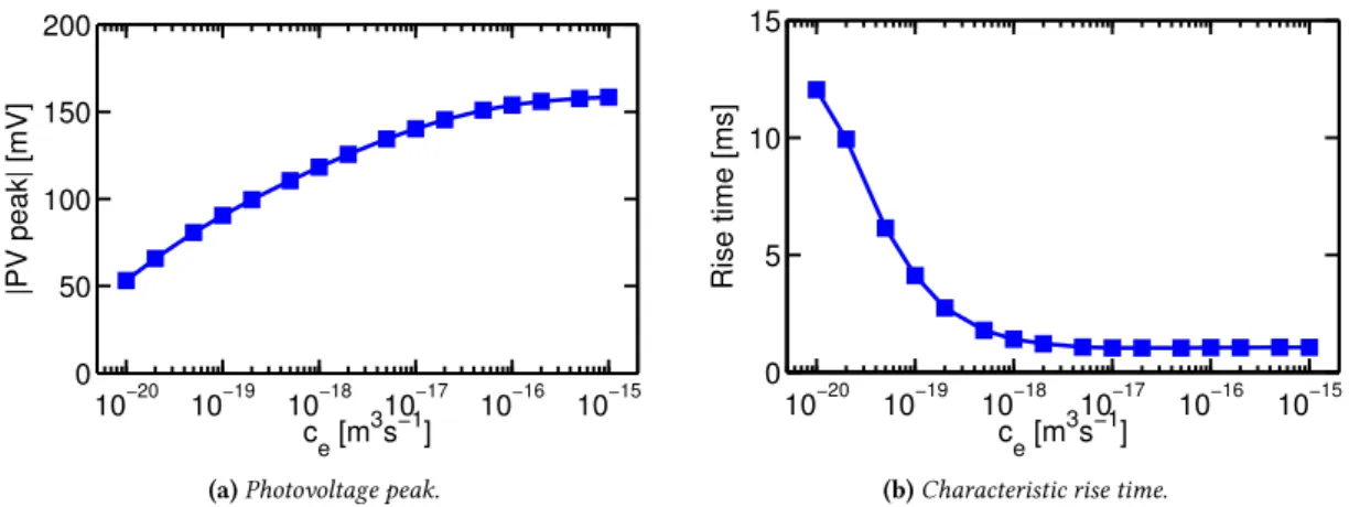
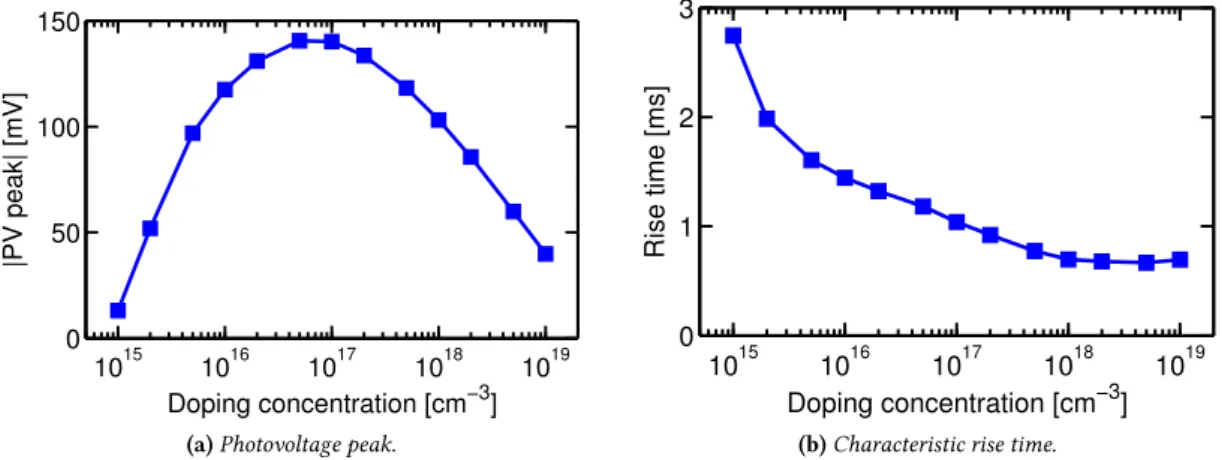
2.4.4.3 Changing the electron capture rate constants cp e and c n e 59 2.4.4.4 Changing the hole trap density (oxygen doping concen-tration) Np t . . . 60
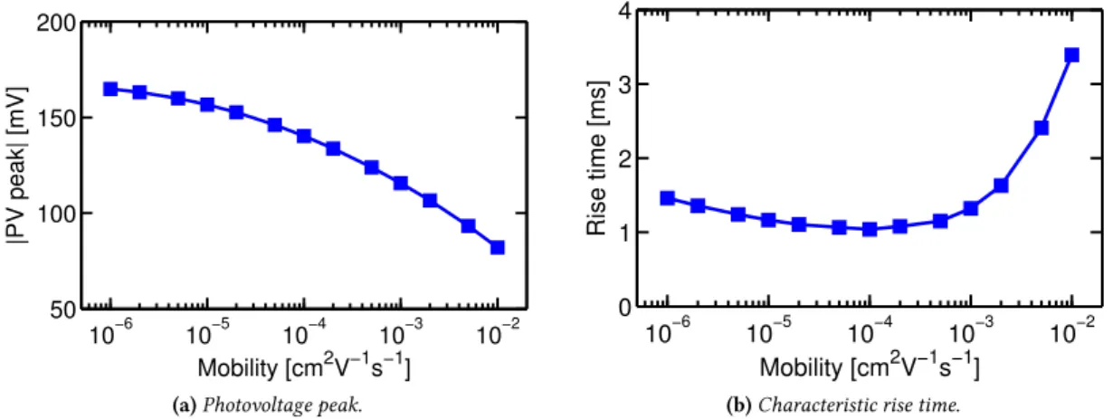
2.4.4.5 Changing the charge carrier mobilities µp,0and µn,0 . . 61
2.4.4.6 Changing the trap depths ∆Ep t and ∆E n t . . . 62
2.5 Lumped model for the photovoltage measurements . . . 63
2.5.0.7 Approximation of R kdissX . . . 67
2.5.1 Numerical results . . . 69
2.6 Surface potential measurements . . . 71
2.6.1 Changing solution molarity . . . 72
2.6.2 Changing incident light power density . . . 73
2.6.3 Changing polymer layer thickness . . . 74
2.6.4 Lumped parameter circuit model . . . 75
2.6.5 Numerical results . . . 77
2.6.5.1 Changing solution concentration . . . 78
2.6.5.2 Changing light power density . . . 80
2.6.5.3 Changing polymer thickness . . . 81
3 Thermally induced effects 83 3.1 Patch clamp measurements . . . 83
3.1.1 Cell membrane . . . 84
3.1.2 Patch clamp technique . . . 85
3.1.3 Patch clamp measurements . . . 87
3.2 Temperature measurements . . . 93
3.3 Heat diffusion modeling . . . 95
3.3.0.1 Numerical implementation . . . 97
3.3.0.2 Numerical results . . . 98
3.4 Patch clamp measurement model . . . 99
3.4.0.3 Numerical results . . . 101
3.4.0.4 Interpretation of the high variability of the fitted values of αV . . . 104
3.5 Approaches to describe temperature dependent capacitance . . . 105
3.5.2 Liquid crystal model and membrane thickness variation . . . 114
4 Finite element methods 117 4.1 The 1D model boundary value problem . . . 118
4.2 Unique solvability and maximum principle . . . 118
4.3 The primal-mixed finite element approximation . . . 119
4.3.1 Finite element spaces . . . 119
4.3.2 Basis functions . . . 119
4.3.3 Finite element formulation . . . 120
4.4 Stability analysis . . . 122
4.4.1 Stabilization in the reaction-diffusion case . . . 123
4.4.2 Stabilization in the advection-diffusion case . . . 123
4.5 Convergence analysis . . . 124
4.6 Conservation properties of the primal-mixed method . . . 126
4.6.1 Conservation for the continuous problem . . . 126
4.6.2 Conservation for the the discrete primal-mixed problem . . . 127
4.7 Finite element approximation in axisymmetric geometries . . . 128
4.7.1 Model problem in an axisymmetric configuration . . . 128
4.7.2 Spatial discretization . . . 133
4.7.3 Convergence analysis on a test case for the Octave library . . . . 138
5 Conclusions and future research perspectives 141 5.1 Conclusions . . . 141
5.2 Future perspectives . . . 144
CHAPTER
1
Introduction: cells, polymers and light
1.1
Bioelectronics and organic semiconductorsBioelectronics is the field of scientific research in which, as its own name suggests, electronic engineering principles are applied to biology, medicine and health sciences, and in the latest years the hype around it, both in the public opinion and in the sci-entific community, considerably grew as a consequence of the tremendous amount of achievements in terms of new materials, devices and understanding of living matter.
The birth of bioelectronics is usually dated to the pioneering work of Luigi Gal-vani in the 18th century, and his famous experiment in which the detached legs of a frog were made move by applying a small voltage. Since then many results have been obtained in directly interfacing artificial materials and biological elements, exploiting the numerous advancements of the rapidly expanding silicon technology. Research activity led to bioelectronic devices that may operate principally in two directions. In one configuration, the biological events alter the interface properties of the electronic elements, thus enabling a readout of the phenomenon by monitoring a particular de-vice property. In a second configuration, instead, the bioelectronic systems use the electronic units to activate the biomaterials towards a particular desired function.
Most activities in this field are related to the development of biosensors, that con-vert recognition or catalytic processes mediated by cells in the form of electronic sig-nals, and lab-on-chip devices [6, 72, 76, 118]. Another prolific research branch is that dealing with the electrical interfacing of neuronal networks with semiconductor mi-crostructures. Neuronal activity can be monitored with semiconductor devices, open-ing the way to hybrid systems for dynamic memory and active learnopen-ing. Conversely, the semiconductor devices can induce cellular response by applying electric signals, the ultimate application being the neural interfaces of prosthetics devices [58,96].
In the latest decades organic semiconductors have emerged as a novel and alter-native class of materials in the electronics field, and among this group we name small molecules and conjugated polymers to have been key players of a sort of revolution in electronics and optoelectronics. Research efforts got great impulse and have been di-rected to explore the possibility for this technology to obtain better performance than the silicon based one and to replace this latter in the fabrication processes. The joint effort in materials chemistry, fundamental research and device engineering led to the demonstration and the commercialization of a new generation of devices, including light emitting diodes, transistors and photovoltaic cells [57,70, 80].
Compared to inorganic semiconductors, organic materials offer attractive charac-teristics in terms of mechanical properties, possibility of chemical engineering and interaction with visible light. Importantly, the technology required for processing materials and realizing devices is relatively cheap and easy, and it fits well with trans-parent, bendable, rollable and lightweight plastic substrates [56]. The counterbalances to be paid back are reduced electronic transport properties and poor environmental stability. Major efforts are currently focusing on improving the performance of so-lar cells and transistors, which are expected to represent the next applications to be delivered on the market.
At the same time, organic electronics is now experiencing a second birth with the combination with bioelectronics. The term “organic bioelectronics” was used for the first time in 2007 by Berggren et al. in a seminal review [16]. The turning point of conducting and semiconducting polymers for biological applications occurred when researchers started to use them as active, functional materials, opposed to the previous usual adoption limited to the role of passive components for coatings. Since then, the field has been growing at a surprisingly fast rate, as documented by the increasing number of publications and funded projects in the field.
The strong interest in organic bioelectronics manifested by the community stems from the fact that in this field no technology predominance is established so far [116, 122], since traditional technologies fail or represent the limiting factor of the device operation, while organic semiconductors do have specific advantages with respect to inorganic materials, offering innovative and valuable solutions. Most importantly, or-ganic semiconductors, and more specifically conjugated polymers, are characterized by a low degree of toxicity, so they show superior biocompatibility and adaptability to work at the interface with living tissues. As mentioned above, their processing in-volves simple and cheap steps, usually performed at low temperature and from liquid phase, allowing deposition on virtually any plastic or soft substrate, which suits the non-planar form factors often required for in-vivo applications. At the macroscopic level, soft polymers offer better mechanical properties than traditional (hard) elec-tronic materials and their surface represents an ideal substrate for growing cells on or for interfacing with extremely delicate tissues. At a sub-microscopic level, their pecu-liar conjugated structure, constituted by alternating single and double carbon bonds, is indeed very similar to the structure found in many biological molecules, and can be conveniently chemically engineered to extend the functionalities and improving per-formance. Moreover, the weak van der Waals bonding, typical of organic materials, leads to intimate interfaces with electrolytes without dangling bonds or oxide lay-ers [66], so this class of materials offlay-ers the unique capability of mixed electronic and
ionic conduction [139], thus opening a new interconnection perspective with living matter.
All the above mentioned properties make organic semiconductors extremely at-tractive for applications in biomedical engineering, neuro-technology and life sci-ences. In few years, many devices have been developed and demonstrated to work both in-vitro and in-vivo, and in some cases they outperform standard, inorganic tech-nologies, and already reached the necessary development for pre-clinical and clinical application. In the following, we present some examples of the developed devices, mostly intended for cellular electric activity elicitation and/or recording, and we di-vide them in three classes: conductive organic bioelectrodes, organic electrochemical transistors and organic field-effect transistors. In section 1.2, we describe emerging techniques and devices for optical stimulation of cell activity, especially focusing on hybrid bio-opto-interfaces, sensitive to visible light, which represent the specific topic of this thesis. The organic-based cell photo-activation represents a completely new tool in the neuroscience field and is especially promising for the realization of an all-organic artificial retinal prosthesis.
1.1.1 Conductive organic bio-electrodes
Traditionally, metals and inorganic semiconductors such as gold, platinum and silicon, have been used to fabricate the electrodes in bionic devices for sensing and stimulation tasks. Such elements show considerable limitations which are mainly constituted by their rigidity and sharpness, which damage or exert chronic stress on the tissues and the surrounding environment, leading to inflammatory reactions, rejection or break-age. In addition the characteristic signal-to-noise ratio is not optimal and the materials are not stable in time and prone to rapid degradation.
Semiconducting polymers were first used as coatings of electrodes, and they proved to successfully meet the requirements of an ideal bioelectrode, namely, low impedance and high biocompatibility [116]. Mechanical contact is improved by reducing the mismatch at the interface with the tissue while the lifetime of the implant is in-creased [73, 90], and, additionally, polymer molecules can be specifically function-alized in order to stimulate cellular outgrowth and minimize the immune response.
Most materials used for this application belong to the class of polythiophenes and biocompatibility has been widely demonstrated in a number of cells. In particular, PE-DOT:PSS, a heavily doped p-type organic semiconductor, has emerged as the reference material for neural interface applications, thanks to its optimal properties of conduc-tivity, chemical and electrical long-term stability, relatively low interface impedance and ease of processability. Biocompatibility of PEDOT was first reported by Mar-tin and coworkers with the fabrication of neuro-electrode interfaces with neuronal cells [137,138]. The reduced impedance of the contact prompted the use of PEDOT:PSS for the fabrication of single electrodes as well as microelectrodes arrays (MEAs) in flex-ible and bendable configurations [19], see e.g. figure 1.1a. In this way a new family of implantable electrodes able to conform to the curvilinear shapes of organs has been developed. As an example Malliaras and coworkers successfully employed a similar MEA to record electrophysiological activity in cerebral cortex with high accuracy, out-performing plain gold electrodes of similar geometry [90]. This important result will
(a)PEDOT electrode (b)Organic field-effect transistor
Figure 1.1: (a) Picture of a PEDOT electrode on a flexible substrate (reproduced with permission from [152]); (b) Schematic diagram of an Organic Field-Effect Transistor (reproduced with permission from [15]).
certainly open the way to other proof-of-concept devices, and since nowadays the actual possibility of progress in neuroscience and medicine strongly relies on find-ing new materials and available technologies, organic-based bioelectrodes will most probably represent the first field where polymers can find a practical use at the clinical level. Potential applications in neurosurgery have been indeed recently highlighted in an interesting perspective by Von Holst [167], including epilepsy, dysfunctions of central and peripheral nerves, traumatic brain injuries and intracranial tumors.
Besides electrodes intended for stimulation and recording, the use of transistors is emerged as a useful tool to extract small electric voltages generated by cell cultures and tissue slices, providing a better signal-to-noise ratio due to local amplification by the transistor circuitry. However, the use of inorganic transistors in in-vivo config-urations has been so far severely hampered by their poor biocompatibility. Organic electronics is rapidly emerging as a valuable alternative, and two kinds of device ar-chitectures have been reported, namely, the Organic Field Effect Transistor (OFET) and the Organic ElectroChemical Transistor (OECT).
1.1.2 Organic field-effect transistors
OFETs have been widely used for the realization of biosensors in the latest years, and many applications have been reported, including pH, glucose, cholesterol and enzyme sensing. Several architectures have been considered, e.g. liquid-gated configurations or by using high capacitive gate dielectric materials, in order to let the device able to operate at very low voltages, see figure 1.1b. This is in biological applications a clear advantage over inorganic technology, since it avoids harmful electrochemical degra-dation and reduces the heat released to the surrounding environment [37]. Among the other advantages of OFETs we mention the possibility of the fabrication of bendable and rollable devices [149,153], using low processing temperatures and simple printing technologies, such as screen printing and ink-jet printing, and, not less importantly, transparency and thermal stability.
The first achievements in using organic transistors for stimulating excitable cell activity are attributed to Stieglitz and coworkers since they used pentacene transis-tors with silicon oxide as dielectric to stimulate a frog sciatic nerve [53], but in that case a strong applied potential was still required. Very recently, Biscarini et al. [38] showed that a liquid-gated pentacene transistor is able to both stimulate and record the extracellular activity of stem murine cells cultured on top of the active polymer layer. The device operated at very low voltages and the OFET response was moni-tored during the different phases of the cell differentiation process, and only when stem cells were differentiated into neurons, it was possible to measure electrical sig-nals upon external stimulation. Muccini et al. [15] demonstrated that a transparent organic transistor was able to provide both stimulation and recording of dorsal root ganglion primary neurons. Such device was characterized by a very good signal-to-noise ratio exceeding by 16 times that of standard microelectrode array systems, and the good properties shown in multi-cell activity recording and stimulation allowed the authors to be optimistic for the use of the device even in single cell recording. 1.1.3 Organic electrochemical transistors
Unlike standard OFET structures, where the active material is separated from the elec-trolyte by an insulating layer, in an OECT device the semiconducting polymer is in direct contact with the electrolyte, see the schematic representation of figure 1.2a. Basically, the OECT device acts as a transconductance amplifier that converts a volt-age modulation at the gate to a modulation of the drain current. At present, the most widely used material in OECTs is PEDOT:PSS, thanks to its superior conduc-tivity (both electronic and ionic carriers are transported) and biocompatibility, and the transconductance has been recently reported in the mS range [93] up to frequen-cies of the order of 1 kHz, a value two orders of magnitude larger than that of planar silicon-based FETs.
OECTs raised interest in the community mainly as biosensors [104], being em-ployed, for instance, in DNA [172], enzymes [176] and cell attachment sensing [20]. The possibility to realize OECT arrays by lithographic processes was first demon-strated in [92], operating at low voltages and showing a response time of the order of 100 µs, thus compatible with biological processes recording, and used in-vivo in cor-tical measurements [91]. Impressively, flexible transistor arrays positively compared with surface electrodes and even with conventional penetrating electrodes, showing superior signal-to-noise ratios, since OECTs locally amplify the signal while conven-tional electrode recordings can only be amplified in a second moment, increasing also the magnitude of the noise.
Another device that exploits the principle of OECTs, is the Organic Electronic Ion Pump (OEIP) developed by Berggren and his collaborators [83]. The device structure consists in two PEDOT:PSS electrodes patterned on a plastic substrate and connected by a channel made by over-oxidized PEDOT:PSS, which is an electric insulator while preserving the capability of conducting ions. Two different solutions are put in con-tact with the electrodes and the source electrolyte contains ions to be delivered to the target one, see figure 1.2b. Oxidation of the source electrode (anode) forces ions to enter the anode itself from the source electrolyte. Since the channel allows ionic
(a)Organic electrochemical transistor (b)Organic electronic ion pump
Figure 1.2: Schematic diagram of (a) Organic Electrochemical Transistor (reproduced with permission from [93]); (b) Organic Electronic Ion Pump (reproduced with permission from [156]).
conductivity, ions are pumped towards the cathode and finally delivered to the target electrolyte. Since ionic charges transported through the channel are compensated by electronic charges flowing between the two electrodes in an external circuit, the out-put current represents a measure of the ion delivery rate. In a biological application, an important advantage over devices based on electrical stimulation is that the ions to be delivered can be appropriately selected in order to target only a specific type of cell that expresses the corresponding receptor. Also charged biomolecules relevant for neuronal cell signaling can be delivered with this device and notable examples re-ported in in-vitro studies include acetylcholine, aspartate, GABA and Glutamate [83]. OEIPs were also fabricated on flexible substrates, suitable for surgical implantation, and the controlled delivery of neurotransmitters was assessed in the cochlear system of guinea pigs, thus demonstrating the possibility to modulate sensory functions in a very specific and quantitative way [156].
1.2
Light mediated cell stimulationIn section 1.1 we reviewed the leading bioelectronics techniques that involve organic materials. Surprisingly, despite their success in photovoltaic and LED technology, the most appealing properties of organic semiconductors, namely their light absorption and emission in the visible spectrum have not been fully exploited in designing new bio-organic interface devices and developing stimulation protocols driven by light in-puts instead of electrical ones.
Indeed, only recently organic semiconductors, working in a photodetector-like configuration, have been proposed as photoactive materials for optical excitation of neurons [64], and later extended to astrocytes [14] and retinal explants [62, 65]. This new approach to light mediated cell stimulation is very promising since it proved to be highly effective though being based on simple devices structures and working principles, and all the activities described in the present thesis have been focused to identifying and understanding the involved phenomena. However, before proceeding to a more detailed description of the technique, a review of the other already available and competing approaches for light mediated cellular stimulation is in order.
1.2.1 Existing technologies
A first group of methods for light-mediated cellular stimulation is based on direct op-tical simulation of the cells. Except for few notable exceptions, like the photoreceptors in the retina, mammalian cells usually do not have a specific sensitivity to light, how-ever, interaction of light with biological tissues, especially neurons, has been broadly reported in the literature. In his seminal work in 1971, Fork demonstrated the possi-bility of photostimulating nerve cells of the marine mollusk Aplysia californica with laser lights both at 488 nm and 515 nm [55], but the mechanism behind the effect was not clear. Since then, several methods have been proposed using light wavelengths ranging a wide part of the spectrum, and aimed at exciting either particular cellular parts or appropriate external absorbing systems used to sensitize the cells. The main advantage of these methods is their simplicity, however, their practical applicability is limited by the high light power usually needed, which can cause mechanical or biochemical stress to the cells.
In this context, the most interesting alternative is Infrared Neural Stimulation (INS), first proposed in 2005 by Wells and coworkers [168, 169]. The technique is based on irradiation of the system with infrared light, below the threshold for tissue damage, and it has been proven that INS is able to stimulate electrical activity in different types of neuronal preparations, both in-vitro and in-vivo [12, 84, 135, 154]. The basic working principle is the IR light absorption by water, which generates a local heating of the preparation. This increase in temperature can have several effects on the cells, and Shapiro et al. proposed a general mechanism based on the variation in the cell membrane capacitance [154]. However, also ion channels have a behavior which is temperature-sensitive and this can take part in the excitation mechanism [3].
A different approach followed by some investigators is to develop particular photoi-somerizable compounds that are able to attain conformations with differences in func-tionality upon light absorption [101]. An example is represented by the acrylamide-azobenzene-quaternary ammonium, a kind of azobenzene derivative, that can revers-ibly switch between a cis- and a trans- configuration, upon light illumination with suitable wavelengths (e.g. UV for trans- to cis-, visible for cis- to trans-) within a mi-crosecond. The trans- configuration binds to cellular K+channels, blocking potassium flow and increasing the cell excitability, while in the cis- form cell activity is reduced, and this has been exploited to restore light sensitivity in blind mice retina [129,163].
The principle of photoinduced change of conformation is also at the basis of molec-ular cages [30,87,119]. One can imagine this structure as a photostable molecule placed inside a photosensitive cage of molecular dimension. This complex can then be intro-duced near or within the cell of interest, where light at a particular wavelength can be used to open the cage by inducing a change of its conformation and to release the trapped molecule. In this way, local concentration increase of particular substances is allowed and it is possible to probe the consequent response of living cells. The ma-jor advantage of this approach for neuronal stimulation consists in the possibility to stimulate only the region where the compound is activated. However, limitations of the method include the inability to reverse the process, limited tissue penetration of UV light and diffusion of the active compound.
stimulation of specific photoactivable probes expressed in cells upon genetic modifica-tion [174]. Up to now, a number of probes can be used to modulate the activity of cells including trans-membrane channels [22], pumps [31], and receptors [2], inhibitors of neurotransmitter release [103] and light-gated protein-protein interaction [102]. Optogenetics represents a powerful technique in neuroscience since it allows the ma-nipulation of the function of specific cell populations of selected regions with high temporal and spatial resolution. However, there are still some issues that have to be solved, in particular, safety concerns regarding the use of viruses for gene expression and the achievement of stable and controlled long-term heterologous protein expres-sion still represent the major challenges.
Optical cell stimulation can also be obtained following indirect pathways, using exogenous photo-absorbers, as an example nanoparticles of semiconducting quantum dots (QDs), The use of cadmium sulfide and cadmium telluride QDs directly binding cells was proposed for the first time by Schmidt and colleagues back in 2001 [170], but effective photostimulation was obtained only several year later using mercury telluride QDs thin films as culturing substrates [123]. Stimulation was attributed to faradaic currents due to charge transfer reactions occurring between the QDs and the extracellular solution, but following work proved that the triggering process is medi-ated by the local electric field genermedi-ated by the excited nanoparticles [175]. Addition-ally, the possibility to control cellular dynamics with nanoparticles of noble metals in in-vitro cultures has been demonstrated [81]. The main concern in the systematic application of QDs regards their possible toxicity, which can arise from different fac-tors, like the particle chemical composition, their geometrical properties or the type of ligands employed. While in some applications the use of QDs has been proven to be safe, there is the need for a standard protocol to address this very important issue. Finally, a novel use of nanoparticles has been proposed by the group of Shoham [52], exploiting thermal stimulation mediated by specifically designed photoabsorbers, namely, iron oxide microparticles, dispersed in the vicinity of the cells to be activated. With this method, high spatial and temporal resolution have been achieved and simi-lar results are obtained also using carbon microparticles.
To conclude this review, cellular photostimulation can be achieved using semi-conductor substrates, and the first approach is attributed to Goda et al. [35]. In their approach cells are grown onto a silicon layer and a voltage is applied between an elec-trode below the substrate and a reference in the extracellular solution. Upon illumi-nation with intensity usually in the order of few mW mm−2, conductivity of minority carriers does increase, and modulating the external bias and illumination intensity, an alternating photocurrent is produced in the device, which is capacitively coupled to the cell membrane. With this approach the selective stimulation of neurons is achiev-able irrespectively of their location on the substrate [67], but the method is appli-cable also to non-neuronal cell types, including muscles, secretory cells and cardiac myocytes [28]. Other photoconductive substrates have considered, including single crystal [158] and hydrogenated amorphous silicon [159], and more recently a TiO2 nanocrystalline film has been used [160].
In general, photoconductive stimulation is a cost-effective, simple and easily im-plementable technique, which can be coupled in a straightforward way in any
stan-dard set-up for electrophysiology. On the other hand, this technique requires high intensity illumination densities and the application of an external bias, both possibly leading to tissue heating and cellular damage. Moreover its applicability in-vivo is difficult, due to limited biocompatibility, the need for electrical wiring, mechanical rigidity and biostability issues. An interesting alternative is represented by silicon-based photovoltaic systems and, as an example, Palanker and his group demonstrated the possibility to realize a wireless, photovoltaic retinal prosthesis, with high pixel density, subretinally implantable and able to induce robust cortical responses in nor-mal and degenerate rats [107,110].
1.2.2 Light mediated cell stimulation with semiconducting polymers
Since the first experimental studies that coupled organic hybrid solid-liquid photo-diodes with light excitation [4, 60, 61], it has been clear that such devices were very suitable for application in a biological framework. However the first demonstration of light-induced modulation of membrane voltage using organic semiconductors can be found in the work by Lanzani and coworkers in [64]. In that work the device struc-ture comprised a layer of a blend of poly(3-hexylthiophene) (P3HT), a photoactive polymer, and phenyl-C61-butyric-acid-methyl ester (PCBM), deposited on an Indium-Tin-Oxide (ITO) covered glass, and immersed in a saline solution, reproducing the ex-tracellular medium. Hippocampal rat neurons were then successfully grown onto the device, previously coated with poly-L-lysine to enhance cell adhesion, see figure 1.3a. The stability and the biocompatibility of the substrate were proved by the fact that after 28 days in-vitro the optoelectronic properties of the active material were not af-fected, and the biological functionalities of the neurons, in terms of cell viability and resting membrane voltage, were not significantly different with respect to control cul-tures. By recording membrane potentials using patch-clamp technique in whole-cell and current-clamp configuration, it was shown that a 20 ms green light pulse (532 nm, 10-15 mW mm−2) evoked the generation of action potentials in neurons with great re-producibility, see figure 1.3c. The response time was very rapid (around ten millisec-onds to reach the peak of the spike) and the photo-stimulation process was highly spatially selective. Upon moving the light spot just outside the cell body, no signifi-cant activity could be elicited in the neuron (figure 1.3b).
The photophysics of the photovoltaic blend used in this study suggests a role for bulk charge photo-generation in the excitation mechanism. However, it has been found that the same transduction process of light pulses into neuronal electrical ac-tivity is obtained using a pristine P3HT film deposited on an ITO covered glass sub-strate [65]. This observation indicates that the working principles of such hybrid interface can be quite different from those of conventional organic photovoltaic de-vices, and that faradaic currents injected in the cleft between the device and the neu-ron, which have been successfully recorded with the same device configuration under continuous illumination [99], are not relevant here for the device operation. Indeed, a large body of experimental evidence suggests the presence of a capacitive coupling between the organic layer and the neuron grown on top of it.
It is important to highlight that the working principle of cell photoactivation is not limited to primary neuronal networks, in fact, the possibility of modulating in a controlled way the whole-cell conductance in primary rat astrocytes by means of
Figure 1.3:(a) Scheme of the photosensing interface, with the neurons grown on top of the active layer and patch-clamp setup. (b) Spatial selectivity of the photostimulating organic interface: a grid of 9 spots (diameter 20 mm was overlaid to a patched neuron and the elicited spikes counted. (c) Generation of action potentials upon photostimulation by a pulsed light train of 20 ms at 1 Hz (green bars) (From [64]).
optical stimulation, properly mediated by the active polymer film, has been recently demonstrated in [14].
The present approach is very general in its working principles and represents a new tool for neural active interfacing, as a simpler alternative to the existing and widely used neuron optogenetic photostimulation techniques able to avoid potentially hazardous gene transfer protocols. The photostimulation is not specific for selected neuronal populations, as is the case for genetically encoded approaches, but the optical stimulation of neurons could be micrometrically shaped to stimulate selected neuronal populations owing to the high spatial selectivity of the photostimulation interface, and could lead to the development of new artificial optoelectronic neurointerfaces based on biocompatible organic materials.
1.2.3 Possible working principles of the device
The working principles of hybrid organic photodiodes may be considerably different with respect to those of conventional ones, mainly because of the interface phenomena occurring between the polymer film and the electrolyte. Most importantly charge transport may have both electronic and ionic nature, and chemical reactions might occur at the interface.
The experimental evidence obtained so far in the works devoted to analyze this kind of structure [60, 61, 64], suggested the authors to describe the device working principles in terms of phenomena of electric nature. Upon photostimulation, excess charges are generated in the active layer and, due to an unbalance in carrier trans-port properties, which depends on the particular choice for the photoactive material (donor/acceptor blend, pristine material), they reorganize determining a charge
dis-OH‒ Cl‒ Cl ‒ OH‒ Na+ K+ Na+ H+ H+ ‒ ‒ ‒ ‒ ‒ ‒ + + + + +
hν
K+ + Active layer ITO/Glass Solution Cell Pipette(a)Electric effects
OH‒ OH‒ Cl‒ Na+ K+ Na+ H +
hν
K+ Cl‒ OH‒ Cl‒ Heat (b)Thermal effectsFigure 1.4:Proposed device working principle based on (a) electric and (b) heating effects.
placement. This in turn is responsible of the establishment of the measured photovolt-age and of a consequent reorganization of the ion distributions in the solution cleft between the substrate and the cell. This ultimately determines a modification of the solution configuration close to the extracellular face of the cell membrane, resulting in its depolarization that might elicit an action potential. In figure 1.4a we report a schematic picture of this process.
However, also heat related phenomena might play an important role, as in the case of the INS technique described in section 1.2.1. For high light intensities, light absorp-tion in the polymer layer might induce temperature increase in the soluabsorp-tion, which in turn might determine modifications in the membrane properties, see figure 1.4b. Should this picture be confirmed, the main advantage of this stimulation technique over INS would be the fact that light absorption occurs in just a few nanometers (against several millimeters of water) so the temperature gradients would be more localized and less power input would be needed.
Up to now, none of these two possible working principles has been shown to be pre-dominant in determining the device operation yet, and a full and accurate description of all the involved steps is still to be provided. In this picture, the present thesis work is aimed at analyzing the above mentioned electric and thermal phenomena occurring in the hybrid device upon illumination, and to do so we want to address to them singu-larly, in order to isolate their respective contribution to the overall operation. Using the insight that experimental evidence provides, we then formulate suitable model descriptions of the device working principles and translate them into mathematical terms in order to quantitatively reproduce the measurement outputs using numerical simulations.
1.2.4 Advanced applications: retinal prosthetics
The phenomenon of cell stimulation by polymer photoexcitation, the high spatial and temporal resolution of the device, together with the good biocompatibility properties demonstrated for the organic semiconductors, open the way to potential applications in the field of retinal prosthetics [109].
The final goal is to restore photosensitivity in retinas whose natural photoreceptors are damaged or lost. However, the retinal photoreceptors behave quite differently
Figure 1.5:(a) Confocal images of control (left) and degenerate (right) retinal sections (gcl: ganglion cell layer; inl: inner nuclear layer; onl: outer nuclear layer; scale bar 50 µm). (b) Schematic representation of the normal and degenerate retina structure. (c) Multi-unit activity recorded upon light stimulation (10 ms, 4 mW mm−2) of a control retina over a ITO:glass substrate (left), a degenerate retina over a
ITO:glass substrate (middle) and a degenerate retina over a P3HT-coated ITO:glass substrate (right). The bottom histograms show normalized post-stimulus time. Green bars/arrows represent the light stimulus (from [65]).
from primary brain neurons since they do not develop action potentials, and, as a whole, retinal physiology is very complex, so a success of a similar approach is far from being taken for granted.
Nevertheless, Benfenati and coworkers reported that such a bio-organic interface is actually capable of restoring light sensitivity in blind retinas ex-vivo [65]. Acutely dissected retinas from albino rats with degenerate photoreceptors were placed on a single-component organic film of P3HT deposited on a ITO:glass substrate in a sub-retinal configuration, i.e. the degenerate photoreceptor layer contacted the polymer, see figure 1.5a.
Multi-unit activity recordings, performed with an extracellular electrode in the reti-nal ganglion cell layer and representing the response of the retina to light, showed that a 10 ms light pulse (4 mW mm−2) was able to stimulate intense activity, at levels indistinguishable from those of control retinas of normal rats, while no significant ac-tivity could be recorded in blinded retinas placed on ITO:glass substrates (figure 1.5c). The analysis of the temporal characteristics of the excitation proved that ganglion cell spiking was mediated by the activation of the external cell layer in contact with the polymer.
Dose-response measurements (figure 1.6) revealed a threshold intensity for pho-tostimulation of about 0.3 µW mm−2, closely matching the range of retinal irradiance during outdoor activity (0.1-10 µW mm−2). In contrast, degenerate retinas recorded over ITO:glass displayed low levels of spiking activity only at very high light inten-sity (threshold 80 µW mm−2, figure 1.6). Another interesting feature is related to the linear dynamic range of operation, which spans 2 log units of retinal irradiation (1-100 µW mm−2). This linear operating range allows modulation of the retinal output
Figure 1.6: (a) Comparison of mean peri-stimulus time histograms obtained from: control retinas on ITO:glass (black bars); degenerate retinas on ITO:glass (open bars); degenerate retinas on P3HT-coated ITO:glass (red bars) in response to light illumination (10 ms, 4 mW mm−2, green arrow). (b)
Dose-response analysis of the mean retinal ganglion cell firing rate versus light intensity performed in de-generate retinas over P3HT-coated ITO:glass (red circles) or ITO:glass alone (open circles). The dashed line corresponds to the computed maximum permissible radiant power for chronic exposure (from [65]).
depending on the light dose reaching the polymer-retina interface, which is an ex-tremely important requirement in developing artificial prostheses aimed at restoring the physiological function of the retina.
Similar results have been reproduced by Narayan and coworkers [62] with embry-onic chick retina at a light insensitive stage of development using moderate light in-tensities (10-600 µW mm−2), proving the consistency and the applicability of the stim-ulation protocol to different types of retinal tissues.
Although the coupling mechanism between neural cells and the semiconducting polymer is still only partially understood, its potential impact is clear-cut. There are however many open issues, regarding in particular the long term stability of the poly-meric material, the tolerability over prolonged time in-vivo and the optimization of the device response. For this reason, recently, research is being conducted to further explore this possibility by subretinally implanting these devices in an animal model of retinal degenerative diseases, such as the Royal College of Surgeons rats bearing a mutation in the Mertk gene.
CHAPTER
2
Polymer/electrolyte device
In order to study the behavior of the device focusing on the electrical effects that might be responsible of its operation, in the present chapter we consider a simplified de-vice without a cell grown onto it, which consists in a layer of poly(3-hexylthiophene) (P3HT), deposited on a Indium-Tin-Oxide (ITO) covered glass substrate, immersed in a NaCl solution, see section 1.2.2. P3HT is a p-type semiconductor conjugated poly-mer, i.e. it mostly allows the electronic transport of positive charge carriers, which is widely used in photovoltaics due to its remarkable optical properties, most impor-tantly a high absorption coefficient in the visible range of the light spectrum. ITO is instead a conducting oxide which combines high transport properties with optical transparency and ease of processability on thin films.
Two different measurement techniques have been considered, see figure 2.1: • Photovoltage measurements: the change of voltage upon illumination
be-tween the ITO contact (1) and a Ag/AgCl reference electrode (5) in the solution is measured using a potentiostat in open circuit configuration.
• Surface potential measurements: the electric potential variation upon illumi-nation in the solution in close proximity of the polymer interface (3) (about 1 µm) is probed using a glass micropipette.
To better understand the role of the components of the device, the measurements are repeated considering different configurations obtained by changing several critical parameters, such as the thickness of the deposited polymer, the ion concentrations of the solution, the light intensity and direction.
In the following sections we report the results of the above mentioned measure-ments, analyze them to get useful information regarding the working principles of the
Active layer ITO/Glass NaCl Solution Reference electrode Pipette Ag/AgCl
1
2
3
4
5
Figure 2.1:Simplified device structure and performed measurements: (1-5) transient photovoltage; (3-(4)-5) surface potential.
hybrid polymer/electrolyte device, and with this insight we propose a series of models aiming at reproducing the experimental results.
2.1
Photovoltage measurementsThe first type of experimental measures that we consider is a particular kind of tran-sient voltage measurement in which the evolution of the difference of the electric potential between the ITO electrode and the bulk solution is tracked upon illumina-tion.
When the transient response of photovoltaic devices upon light stimulation is ad-dressed, the mainstream adopted techniques are transient photocurrent and photo-CELIV (Charge Extraction by Linearly Increasing Voltage) [17]. Transient photovolt-age technique is less frequently adopted since photovoltaic devices are typically in-tended for the generation of charge current. In the configuration considered in the present work, transient photovoltage is instead perfectly fitting the device operation principles, since the final aim of the polymer-electrolyte interface is that of generating a voltage signal to be transduced to the living cell.
For this reason Narayan and coworkers successfully adopted this particular tech-nique for characterizing a hybrid polymer blend/interface in [60], which shares the ba-sic structure with the device currently under study. In our configuration however, the active layer differs by the fact that only a pristine polymer is considered and addition-ally we adopted a different setup for performing the measurement, that we describe in the following section.
2.1.1 Description of the experimental technique
Electrochemical characterization is carried out by using an Autolab potentiostat/gal-vanostat (PGSTAT) [9, 113], in a three electrode configuration, see figure 2.2, and a basic diagram of this particular setup is presented in figure 2.3.
The three-electrode cell is the most common setup used in electrochemistry, see figure 2.2, and the three electrode are referred to as Counter (CE), Reference (RE) and Working Electrode (WE), respectively.
Figure 2.2:Schematic view of the three-electrode cell setup (reproduced from [113]).
Figure 2.3:Basic diagram of a potentiostat/galvanostat (reproduced from [113]).
the electrochemical cell, it is made of an inert material (in the present case Pt) and it does not participate in the phenomena to be measured.
As its name suggests, the RE is used as a reference point for the potential control and measurement since it has a stable and well-known potential. High stability of the potential is usually achieved by employing a redox system with constant concentra-tions of each participants of the redox reaction, and in the current setup the Ag/AgCl couple in a saturated KCl solution is considered.
The WE is that on which the phenomenon under study occurs, and in the current configuration it is represented by the P3HT-coated ITO substrate.
In potentiostatic mode, the PGSTAT accurately controls the potential of the CE against the WE, so that the potential difference between the WE and the RE is well defined and corresponds to the value specified by the user. In galvanostatic mode, the current flow between the WE and the CE is controlled. The potential difference between the RE and WE and the current flowing between the CE and WE are contin-uously monitored. By using the PGSTAT, the value specified by the user (i.e. applied potential or current) is accurately controlled all the time during the measurement by using a negative feedback mechanism, as illustrated in the circuit scheme of figure 2.3. In the analysis object of this section, we perform measurements of the voltage at the WE in potentiostatic mode, setting the current between the WE and the CE to zero (open circuit). The measurement is performed starting from dark condition and then
0 50 100 0 50 100 150 200 Time [ms] Voltage [mV] 25 75
Figure 2.4:Typical profile of a photovoltage measurement. The shaded area indicates the period of time when the light is on.
illuminating the device using a collimated white LED (MCWHL2-C4, Thorlabs) source with 50 ms pulses characterized by an abrupt on/off transition, with the possibility of modulating the incident power intensity. Data acquisition and analysis is performed using NOVA 1.10 and Matlab.
Measurements performed on devices which are fabricated in order to have the same specifications result however in slightly different outputs since it is very difficult to have a complete control on the device geometry, and most importantly, in the internal structure of the polymer layer (e.g. impurity concentration, local order, roughness). Nevertheless all the measurements share common features that are well represented by the typical photovoltage profile reported in figure 2.4. Before light is switched on, the instrument measures a constant voltage between the electrodes, which is com-monly positive and ranges between a few and one or two hundreds of millivolts. When the device is hit by the light, the polymer absorbs part of it and electrical charges are generated. Consequently an evolution of the measured voltage towards lower values (i.e. the generated photovoltage is negative) with a characteristic time scale of a few milliseconds is observed, due to the rearrangement of the photogenerated charges in the polymer. Since the bath of the solution is taken to be at the reference value of the potential, such change is consistent with a net displacement of negative charge towards the ITO electrode.
Superposed on the fast negative photovoltage transient, the measure shows an-other slower component characterized by an opposite sign. Such behavior has to be ascribed to a charge movement in the opposite direction with respect to that of the fast component, and since the observed time scales are very different it is likely to be attributed to other kind of phenomena characterized by slower rates (e.g. chemical reactions involving electron transfer). Since on the considered time scale of the mea-surements that are about to be shown in the next part of the section such feature is less important than the fast negative contribution, we will neglect it in our analysis.
When light is switched off, the initial configuration of the device is recovered and the measured voltage evolves to the values observed before the illumination. A very important fact is that such relaxation has a characteristic time which is longer than that of the light-on transient. A possible interpretation consists in attributing the
recovery process to phenomena occurring with a low rate, as charge recombination events involving more than one particle or a large energetic barrier to be overcome. 2.1.2 Changing device thickness and illumination direction
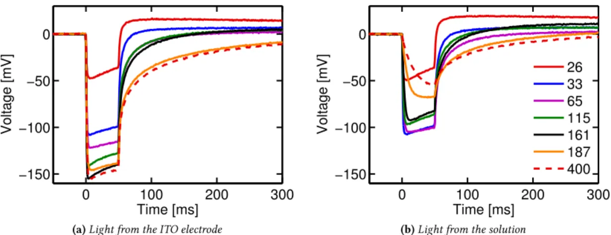
As previously reported, we performed a series of measurements in which we grad-ually varied either one of the parameters of the device or the characteristics of the illumination protocol. In the first set we consider, some devices have been fabri-cated by depositing layers of polymer of different thickness, in the range between 26 and 400 nm, and we performed transient photovoltage measurements shining LED light with power density 267.5 µW mm−2both from the transparent ITO electrode side and the solution side. With these experiments our aim is to understand whether the effects that drive the device behavior are of bulk type or they just occur in the in-terface regions, and, if this latter is the case, which are the different roles of the two interfaces.
The results are reported in figure 2.5a and 2.5b for the cases of illumination from the ITO electrode and the solution, respectively, and the differences between the two illumination protocols are quite evident. For all the traces the initial offset is removed so that the average of each measurement is equal to zero in the pre-illumination pe-riod. In the case of light from the ITO electrode we observe photovoltage transients that are consistently fast for all the considered device thicknesses, see figure 2.6b, whose peak values monotonically increase with larger device thickness. The behav-ior of this increase is nonlinear, with a steeper increase for thin devices and a certain level of saturation for the thickest devices. The case of illumination from the solu-tion side has instead a richer variety of features. The results for the thinnest devices do not differ significantly with respect to the case of illumination from the electrode side, but thickening further the devices we observe that the photovoltage transients become progressively slower and less intense, see figure 2.5b. The photovoltage peak values and the characteristic rise time reported in figure 2.6 are obtained by fitting the experimental results using a double exponential function of the form
V (t ) = −∆V1 " 1 − exp − t τrise,1 ! # −∆V2 " 1 − exp − t τrise,2 ! # (2.1) and by considering the values ∆V1 (> ∆V2) and τrise,1 (< τrise,2) corresponding to the principal fast component of the measurement.
For the interpretation of the results, it is useful to recall here the presumed work-ing principles of the device. When light hits the device, it is in part absorbed by the photovoltaic polymer generating excited states called excitons [69, 70]. These states consist in a strongly bonded electron-hole pair localized on a polymer molecule and for this reason they do not have a net charge. Excitons have a characteristic decay time of a few hundreds of picoseconds and can move in the polymer matrix by diffu-sion events. The hole and electron that form the exciton may eventually dissociate at heterojunctions of materials having different electronic affinity, and this phenomenon is enhanced by the presence of a local electric field [33,69]. However, in pristine mate-rials like the one used in our device, exciton dissociation usually occurs with a limited rate and only the electric field can increase the dissociation probability to apprecia-ble levels. Once free charges are generated, they can migrate following concentration
0 100 200 300 −150 −100 −50 0 Time [ms] Voltage [mV]
(a)Light from the ITO electrode
0 100 200 300 −150 −100 −50 0 Time [ms] Voltage [mV] 26 33 65 115 161 187 400
(b)Light from the solution
Figure 2.5:Transient photovoltage measurements obtained with devices characterized by different thick-ness of the polymer layer (legend reports the values in nanometers).
0 100 200 300 400 0 25 50 75 100 125 150 175 Thickness [nm] Peak voltage [mV]
(a)Photovoltage peak
0 100 200 300 400 0 5 10 15 20 Thickness [nm] Rise time [ms] ITO side Solution side (b)Rise time
Figure 2.6:Photovoltage peak value and characteristic rise time obtained from the experimental measure-ments, for both illumination from the ITO side and the solution side.
gradients (diffusion) or under the action of the electric field (drift) as in traditional solar cells. The main difference with these latter is the fact that no charge is extracted, and for this reason a charge displacement is built up that eventually determines the set up of a photovoltage that blocks further charge migration and leads to a condition of dynamic equilibrium.
With this premise, from the results of figures 2.5 and 2.6 we can draw the first con-clusion that the phenomena that determine the generation of the photovoltage, most importantly exciton dissociation, are not entirely of bulk type and, instead, interfaces must play a key role. Should this not be the case, for each polymer thickness we would expect to measure the same photovoltage, irrespectively of the illumination direction, and hence obtain increasing signals for thick devices also with light from the solution, which clearly is not observed. Moreover, should the dissociation mechanism be the same at the two interfaces, the photovoltage measurements would have opposite sign for the two illumination protocols. This is a clear indication that only one of the two interfaces plays a role in the operation of the device.
generation occurs and how the density of these latter might look like in the device under illumination. When light hits the polymer the first layers absorb part of the incident photons and the remaining are transmitted through the other layers deeper in the bulk. This applies for the entire material, the result being that less and less light is absorbed in the polymer and hence the exciton generation process has a rate which is a decreasing function of the distance from the incidence interface. Since the excitons have a quite short lifetime, the characteristic diffusion length is limited, and the exciton density profile resembles the generation profile, resulting in a high population at the incidence region which decays in exponential way going into the bulk of the material.
The generation rate of free charges at a particular point of the polymer depends on the local exciton density and if we assume that dissociation occurs mainly in the area close to the ITO/polymer interface, it is possible to interpret the photovoltage results of figure 2.5 after the considerations just drawn above. In the case of light from the solution, thicker devices are expected to have a lower exciton density in the area close to the ITO/polymer interface and for this reason also free charges are generated in lower number, with a slower rate. This eventually results in a less intense photovoltage signal which reaches the peak value in longer time, consistently with the observed measurements.
When light hits the device from the ITO side, the exciton density is such region is independent on the device thickness and for this reason the photovoltage should not be affected. Nevertheless, the measurements show that the photovoltage peak slightly increases with thickness and this might be due to dissociation occurring in the bulk material with a rate lower than that of the interface region.
Moreover, it is possible to provide an estimate of the width of the interface dissoci-ation area from the photovoltage profiles obtained with the thinnest devices, namely those with thickness equal to 26 and 33 nm, since they behave in a very similar way irrespectively of the illumination side. For thin devices the spatial decrease of the exciton generation profile is less pronounced and hence it is possible to consider a constant exciton density in the layer. Hence if the number of locally available exci-tons is not the limiting factor for the free charge generation rate and if the exciton dissociation is equally efficient all along the polymer, we should expect photovoltage peak values that uniformly increase with the thickness of the polymer. Since the val-ues in figure 2.6a clearly show that this trend is not maintained after thickness valval-ues larger than 33 nm, this must mean that the high efficiency dissociation region is not much wider than that. As we already pointed out, with thicker devices in the case of light from the ITO the photovoltage peak still increases because more excitons are generated in a larger polymer bulk domain, still with lower efficiency. With illumina-tion from the soluillumina-tion, instead, the overlap between the high exciton density area and the high dissociation efficiency area is progressively reduced.
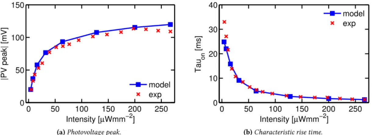
2.1.3 Changing illumination intensity
Another set of measurements is performed on a device with a predetermined thick-ness of about 150 nm, illuminating from the ITO electrode side and changing the LED intensity from 4.68 µW mm−2 to the maximum value achievable with the instrument of 267.5 µW mm−2. The results are reported in figure 2.7.