3
5
CONTENTS
Acronyms and Symbols ... 7
Figures and Tables ... 9
Abstract ... 17
Introduction ... 19
1. Material properties of ZnO ... 33
1.1 n-type conductivity ... 33
1.2 Band structure in the bulk... 35
1.3 Surface band structure and its modification in presence of adsorbates ... 38
1.4 Co-substitution ... 41
2. Materials and Methods ... 49
2.1 Pulsed Laser Deposition ... 50
Experiment ... 53
2.2 Scanning Probe Microscopy ... 55
Atomic Force Microscopy. ... 56
AFM-based Techniques. ... 60
Scanning Tunneling Microscopy. ... 63
Experiment ... 64
2.3 Other Techniques ... 67
Scanning Electron Microscope, Field Emission Scanning Electron Microscope and Energy Dispersive Spectroscopy ... 67
X-Ray Diffraction ... 69
6
3.1 Introduction ... 77
3.2 Structural and morphological characterizations ... 78
Introduction. ... 78
X-Ray diffraction and electron-dispersive spectroscopy of ZnO and ZnCoO thin films. ... 78
Surface morphology and thickness measurements. ... 81
Discussion... 84
3.3 The effect of Co-substitution on the reactive properties of ZnO surface ... 85
Introduction. ... 85
Surface photo-voltage measurements. ... 85
Photo-conductive properties. ... 93
Discussion... 99
3.4 Electro-mechanical and Charge Storing Properties ... 105
Introduction. ... 105
Electro-mechanical properties... 105
Charge Storing effect. ... 108
Discussion... 112
4. Conclusions ... 117
7
Acronyms and Symbols
A-
Negatively charged adsorbates
a
0Intermolecular distance
AFM
Atomic force microscope
ARPES
Angle-resolved photoemission spectroscopy
BCB
Bottom of the conduction band
C-AFM
Conductive atomic force microscopy
CB
Conduction band
CBM
Conduction band minimum
CS
Charge storage
DFT
Density functional theory
DFT+U
DFT with on-site Coulomb interaction
D-V
Cantilever-deflection vs DC-voltage
E
CBEnergy of the bottom level of the conduction band
E
DDonor levels
EDS
Energy dispersive spectroscopy
E
FFermi energy
EFM
Electrostatic force microscopy
E
gBand-gap energy
E
vVacuum energy
f
0Free resonance frequency
F
esElectro-static force
FESEM
Field emission scanning electron microscope
F
intInteraction force
FWHM
Full-width-half-maximum
GGA
Generalized gradient approximation
GW
Green's function and Coulomb interaction approximation
h-e
Hole-electron pairs
HV
High vacuum
KPFM
Kelvin probe force microscopy
LDA
Local density approximation
L-J
Lennard-Jones
MEMS
Micro-electro-mechanical system
PFM
Piezo-response force microscopy
8
PLD
Pulsed laser deposition
P-S
Probe-sample
S
aArithmetic average of roughness profile
SEM
Scanning electron microscope
SPM
Scanning probe microscopy
SPV
Surface photo voltage
S
qRoot mean square
STM
Scanning tunnelling microscope
STS
Scanning tunnelling spectroscopy
TEM
Transmission electron microscope
UHV
Ultra high vacuum
UV
Ultra Violet
V
ACAC voltage
VBM
Valence band maximum
V
CPDContact potential difference
V
DCDC voltage
V
OOxygen vacancy
V
SBand bending potential at surface
W
Work function
XANES
X-ray absorption near edge structure
XRD
X-ray diffraction
Zn
iInterstitial Zinc
z
tSeparation distance between the probe and the sample surface
λ
Wavelength
Φ
Tunnelling barrier height
9
Figures and Tables
Figure 1 19
a Calculated energy diagram of ZnO. b Wurtzite structure of ZnO.
Figure 1.1 35
k|| scans in hexagonal plane of the ZnO Brillouin zone and
comparison between experimental and theoretical band structure. A photon energy of 135 eV was chosen to study the Γ-M-K basal plane. (a) The Γ-M-K plane and (b) its constant-energy contour plot of the photoemission intensity. The red lines denote Brillouin zone boundaries, and the dashed blue lines are connectors to the Γ points. The arrows indicate the sliced directions measured. (c) and (d) Comparison between experimental band structure (grey scale) and theoretical band structure within the GW approximation. The origin of energy is chosen at the conduction band minimum. The red lines represent p-O bands, the green lines hybridized s-Zn/p-O bands, and the blue line d-Zn bands. It can be seen that the d-Zn band is too high, and there is overlap with the s-Zn/p-O bands. (e) and (f) Comparison between experimental band structure (grey scale) and theoretical band structure within the GW with
on-site potential. The d-Zn band is no longer too high, and the
s-Zn/p-O and d-Zn bands do not overlap.
Figure 1.2 39
Band structure of a semiconductor close to the surface and its modification (a) with and (b) without adsorbed charged species.
Figure 1.3 42
Spin-polarized electronic band structure along the H–Γ–M
10
direction, for the neutral (a) and negatively charged (b) Co–VO
complex in ZnO.
Figure 2.1 51
The laser beam (not visible in the picture) hits the target surface, evaporating the material that emerges in a typical shaped plume.
Figure 2.2 53
PLD System at ISC-CNR (Rome). The vacuum chamber is visible on the left side of the image, while the laser source is placed on the upper right
Figure 2.3 55
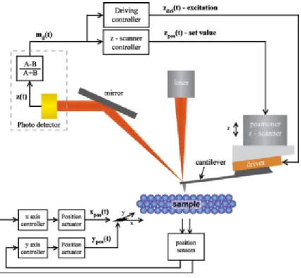
SPM basic setup. The interaction has a functional dependence on probe-sample distance and a feedback system uses the signal acquired from sensor, compared with a setpoint value, to drive a piezo-actuator in order to separate or approach probe to sample, restoring the interaction at the desired setpoint
Figure 2.4 57
Interaction potential sketch of AFM working modes.
Figure 2.5 58
General setup used for AFM and derived techniques. In this case a piezo-tube under the sample provides the raster scanner, while z-scan is effectuated by another piezo actuator behind the tip-holder. In brown, an optional piezo plate is mounted behind the probe in order to provide the cantilever oscillation in alternate contact and
non-contact modes. Sensing equipment is composite by a laser-photodiode
system, able to measure the cantilever deflection.
Figure 2.6 60
Electronic energy levels for (a) probe and sample separated of a distance d, (b) probe and samples in electrical contact with a current I flowing to equilibrate Fermi levels, (c) probe and sample when a DC bias is applied in order to nullify VCPD.
11
Figure 2.7 65
Bruker AFM into its acoustic box with UV equipment on the left side.
Figure 2.8 66
UHV “Omicron RT-AFM/STM” system.
Figure 2.9 68
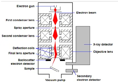
General SEM setup. An electron beam is generated by a filament for thermo-electric emission. Then electrons are accelerated and collimated by electron lenses. Finally the beam is deflected in order to perform the raster scan. A SEM can be equipped by different detectors for several acquisition modes.
Figure 2.10 70
Bragg’s law.
Figure 2.11 70
XRD and FESEM equipment installed at MUSA lab of SPIN-CNR (U.O.S. Salerno) on the left- and right-side, respectively.
Figure 3.1 79
a XRD pattern for ZnO (in black) and ZnCoO (in red). b ω-scan around (002) ZnO peak. c EDS analysis for ZnO (in black) and ZnCoO (in red) samples.
Figure 3.2 80
Topography of (a) ZnO and (b) ZnCoO acquired by means of FESEM, on 3µm x 3µm scan area. Both pure and Co-substituted ZnO show a granular morphology with grain lateral size ranging from 50 to 200 nm. c Transversal FESEM imaging of the ZnO sample. The brighter area is the ZnO film, whereas the beneath darker area is the Si substrate. d Close-up of the ZnCoO surface.
Figure 3.3 81
AFM images, 3µm x 3µm scan size, acquired on (a) ZnO and (b) ZnCoO.
12
Figure 3.4 82
Angular distribution of (a) ZnO and (b) ZnCoO grains, as extracted from Figure 3.3a and b, respectively.
Figure 3.5 86
KPFM maps, 3µm×3µm in lateral size, of ZnO (a) and Co:ZnO (b), acquired in air and dark illumination conditions; (c) VCPD
distributions of ZnO (in blue) and ZnCoO (in red) extracted from a and b, respectively.
Figure 3.6 87
a KPFM maps, 3µm×1µm in size, of as-grown ZnO in dark conditions (top) and under UV-lighting (bottom), acquired in air; b VCPD distributions of dark (green) and UV-irradiated ZnO
(orange) from a statistic of 256×256 points equally distribute on 3µmx3µm scan areas, fitted by Gaussian function; c KPFM maps, 3µm×1µm in size, of ZnCoO in dark conditions (top) and under UV-lighting (bottom), acquired in air; d VCPD
distributions of dark (green) and UV-irradiated ZnCoO (orange) from a statistic of 256×256 points equally distribute on 3µmx3µm scan areas, and fitted by Gaussian function.
Figure 3.7 88
a SPV vs Photon Energy (Light Wavelength) of ZnO (in blue) and ZnCoO (in red); b SPV rise and decay processes measured on ZnO for 3 representative wavelength of 360, 380 and 387 nm. Colour of circlets in a correspond to the same colour curve in b.
Figure 3.8 90
Top: SPV comparison between as-grown and annealed ZnO and ZnCoO. Cropped maps are 1µm x 3µm in size. Bottom: recovering time of SPV in ZnO in air after annealing.
Figure 3.9 92
13
ZnO (in blue) and Co:ZnO (in red), with correspondent second-order polynomial fitting function; b summary of results of KPFM and UHV-EFM experiments, in ambient and vacuum conditions, on ZnO and ZnCoO.
Figure 3.10 94
C-AFM maps at V=0V of 3µm×3µm in size on (a) ZnO in air, (b) ZnO in UHV and (c) in ZnCoO. The colour scale has been equalized to the same range of values for all of the presented maps, in order to facilitate the direct comparison.
Figure 3.11 95
C-AFM maps acquired on (a, c) ZnO and (b, d) ZnCoO of subsequent scanning with grounded probe and 0V bias applied in (a, b) dark and (c, d) UV light conditions. Each frame reports the percentage of scanned area with measured current above |-1 nA|.
Figure 3.12 96
Re-charge process of the ZnO surface investigated by means of 0V bias C-AFM experiments. a C-AFM map after the discharge process of a sub-area (highlighted with a dashed square) and b after 1 hour.
Figure 3.13 97
Main plots: IVs in dark (black) and under UV-illumination conditions (red) acquired on (a) ZnO and (b) ZnCoO. The drastic change in conductivity for ZnO is not present in ZnCoO. Insets: representative IVs showing the behaviour of the conductivity in ZnO and ZnCoO after the UV excitation have been turned off.
14
Sketch of the electronic band structure, for (a) ZnO and (b) ZnCoO. Free electrons in CB, from donor levels (red dots), reduce their energy by moving into lower energy levels introduced by C-VO complexes.
Figure 3.15 100
Spin-polarized electronic band structure along the H–Γ–M direction, for the neutral (a) and negatively charged (b) Co–VO
complex in ZnO.
Figure 3.16 101
Sketch of the energy band structure, close to the surface in ZnO (ZnCoO) (a) as-grown (b) UV-lighted and (c) after-UV.
Figure 3.17 102
Sketch of the electronic band structure, close to the surface in (a) as-grown ZnO (b) annealed or UV-irradiated ZnO (c) ZnCoO.
Figure 3.18 106
a (b) Amplitude maps of PFM acquired on ZnO (ZnCoO). c (b)
Distribution of d33 coefficient for ZnO (ZnCoO) recovered from map a
(b).
Figure 3.19 107
a (b) PFM phase maps acquired on ZnO (ZnCoO). c (d) profile line
extracted across phase maps of ZnO (ZnCoO).
Figure 3.20 109
a AFM topography. b VCPD map before the poling procedure (that will
be performed on the yellow dotted sub-region). c VCPD map after the
poling procedure. d profile line of the poled region along the white dotted line in c.
Figure 3.21 110
a AFM topography. b VCPD map before the poling procedure (that will
be performed on the yellow dotted sub-region). c VCPD map after the
poling procedure. d profile line of the poled region along the white dotted line in c.
15
a VCPD profile line along poled areas for ZnO (in blue) and ZnCoO (in
red) samples. b Behaviour of poled areas in ZnO under UV light conditions.
Table 1 54
Deposition parameters.
Table 2 83
17
Abstract
ZnO is an intrinsic n-type, wide band-gap (3.4 eV at 0 K), semiconductor which has been attracted the interest of the scientific community for several decades. More recently, ZnO has caught a renewed interest due to the improvements in the epitaxial growth techniques as well as to the possibility of p-type conductivity and ferromagnetic behaviour as a consequence of cation doping. In addition to this, as it shows much stronger electric polarization effects than other wide-gap semiconductors, such as GaN and SiC, ZnO has a great potential for manufacturing energy-harvesting systems. Moreover, as ZnO is a semiconducting piezoelectric material, it is already widely used in electro-mechanical systems for making smart sensors and nano-actuators and in communications for surface acoustic wave and thin film bulk acoustic wave resonator devices. However, the potential applications of ZnO as well as of various transition-metal oxides, e.g. TiO2, V2O5, and SnO2, is affected by their electronic structure and surface chemistry. In particular, the material band structure can be properly designed and tuned by electron doping or atom substitution, whereas the stabilization of surface defects, chemistry and reactivity is still a largely unexplored field.
In this work the effect of Co-substitution on the electronic, electromechanical and surface properties of ZnO thin films (50 nm in thickness) has been deeply investigated. The substitution of Zn with Co atoms ensures no electrical doping, since the valence number of Zn and Co is the same. However, a 5% content of Co-substitution in ZnO has been previously shown to be enough to affect the electron conductivity of ZnO and to induce ferromagnetism in the semiconducting oxide. This behaviour has been theoretically addressed to the capability of Co to affect ZnO electronic band structure, by bonding the oxygen vacancies (typical ZnO intrinsic defects), introducing additional spin-polarized electronic levels close to the conduction band edge. Being spatially localized around the Co-complexes, these levels may alter the concentration of free carriers in intrinsically n-type ZnO, hence its bulk conductivity. These effects of Co-substitution on magnetic and conductive
18
properties of ZnO have been recently studied by means of “bulk” experimental (X-ray absorption near edge structure, Hall measurements, magnetization measurements, …) and theoretical investigation techniques (DFT, calculation for isolated defect in a crystal matrix, …). On the contrary, in the case of our nano-sized thin films (50 nm in thickness) it is of fundamental importance to distinguish between “bulk” effect of Co-substitution and surface properties as well as eventual high defect concentration. In this scenario, scanning probe microscopy based experiments, such as conductive atomic force microscopy, electrostatic force microscopy, Kelvin probe force microscopy and piezo-response force microscopy, have been used to study the effect of Co-substitution on ZnO surface reactivity, work function, piezoelectricity and charge storage. The complexity of the observed phenomena required a deep study in different environmental conditions, such as in air and ultra-high vacuum, dark and under monochromatic UV light irradiation. In this thesis, it will be demonstrated that Co-substitution (5% content) deeply affect ZnO work function, leading to a 410 meV downward shift of the Fermi level, towards the valence band, and surface reactivity, inhibiting the adsorption of reactive molecular species at the surface. On the contrary, it does not affect ZnO piezoelectricity and charge storage phenomenon. These findings will be discussed in the framework of existing theoretical model.
19
Introduction
Zinc Oxide (ZnO) is considered as a very promising material for semiconducting device applications1,2. It is a wide band-gap (3.2÷3.4eV at 300K)3,4 metal oxide
semiconductor, with a direct band-gap (i.e. conduction band minimum and valence band maximum occurring at the same k-point, Γ), as depicted in Figure 1a, extending in the near-UV energy region5–9. ZnO crystallizes in the wurtzite structure (Figure
1b) with possibility to have large single crystals10, in contrast with other
wurtzite-like semiconductors as GaN.
Figure 1 a Calculated energy diagram of ZnO4. b Wurtzite structure of ZnO.
Despite the fact that physical properties of ZnO have been studied since the beginning of the semiconductors era4, the lack of control over its electric properties,
as conductivity, (e.g. only n-type ZnO crystals were fabricated with high quality factors up to 1999)4 discouraged researchers in using ZnO to fabricate
semiconducting devices. Over the last two decades, the improvement of quality of ZnO thin films and the possibility to use it as substrate for other materials involved in optoelectronics and electronics (as GaN)1,2,10 drove many research groups
worldwide to control unintentional n-type doping of the material and try to achieve
20
single crystals10, the discovery of exotic nanostructures11, as well as the possibility
to be used in bio-electronics application due to its biocompatibility12,13 made ZnO a
promising semiconducting material for new generation electronics.
Large efforts have been employed also in theoretical studies and in particular on first-principles calculations based on density functional theory for a deep understanding of the role of native impurities, point defects and for band-gap engineering14–27 .
Controlling the conductivity in ZnO has remained a major issue. Even relatively small concentrations of native point defects and impurities (down to 10-14 cm-3 or
0.01 ppm) can significantly affect the electrical and optical properties of semiconductors4. Therefore, understanding the role of native point defects (i.e.
vacancies, interstitials, and anti-sites) and the incorporation of impurities is key toward controlling the conductivity in ZnO. For a long time it has been postulated that the unintentional n-type conductivity in ZnO is caused by the presence of oxygen vacancies or zinc interstitials28,29. However, recent state-of-the-art density
functional calculations corroborated by optically detected electron paramagnetic resonance measurements on high quality ZnO crystals have demonstrated that this attribution to native defects cannot be correct15,16,20,22,26,30. It has been shown that
oxygen vacancies are actually deep donors and cannot contribute to n-type conductivity20,30,31. In addition, it was found that the other point defects (e.g. Zn
interstitials and Zn anti-sites) are also unlikely causes of the observed n-type conductivity in as-grown ZnO crystals22,26. Instead, the cause would be related to the
unintentional incorporation of impurities that act as shallow donors, such as hydrogen which is present in almost all growth and processing environments14–26.
By means of density-functional calculations it has been shown that interstitial H forms a strong bond with O in ZnO and acts as a shallow donor, contrary to the amphoteric behaviour of interstitial H in conventional semiconductors15.
Subsequently, interstitial H has been identified and characterized in ZnO32,33.
However, interstitial H is highly mobile34,35 and can easily diffuse out of the samples,
making it difficult to explain the stability of the n-type conductivity at relatively high temperatures36,37.
21
More recently, it has been suggested that H can also substitute for O in ZnO and act as a shallow donor26. Substitutional H is much more stable than interstitial H and
can explain the stability of the n-type conductivity and its variation with oxygen partial pressure26. Other shallow-donor impurities that emerge as candidates to
explain the unintentional n-type conductivity in ZnO are Ga, Al and In. However, these are not necessarily present in all samples in which n-type conductivity has been observed38. Obtaining p-type doping in ZnO has proved to be a very difficult
task1,2. A reason lies in a lack of shallow acceptors in ZnO. Column-IA elements (Li,
Na, K) on the Zn site are either deep acceptors or are also stable as interstitial donors that compensate p-type conductivity35,39,40. Column IB elements (Cu, Ag, Au)
are deep acceptors and do not contribute to p-type conductivity. And because O is a highly electronegative first-row element, only N is likely to result in a shallow acceptor level in ZnO. The other column V elements (P, As, Sb) substituting on O sites are all deep acceptors39. Quite a few research groups have reported observing
p-type conductivity in ZnO41–47. In order to explain the reports on p-type doping
using P, As or Sb, it was suggested that these impurities would substitute for Zn and form complexes with two Zn vacancies48. One problem with this explanation is that
these complexes have high formation energies and are unlikely to form. In addition, the reports on p-type ZnO using P, As or Sb often include unexpectedly high hole concentrations, and contain scant information about the crystal quality of the samples or the stability of the p-type conductivity41–47.
On the other hand, the wide range of useful properties displayed by ZnO has been recognized for a long time4. What has captured most of the attention in recent years is the
fact that ZnO is a semiconductor with a direct band gap6–8, which in principle enables
optoelectronic applications in the blue and UV regions of the spectrum. The prospect of such applications has been fuelled by impressive progress in bulk-crystal49,50 as well as
thin-film growth over the past few years43,47,51–54. A partial list of the properties of ZnO
that distinguish it from other semiconductors or oxides or render it useful for applications includes:
Intrinsic n-type. The as-grown ZnO bulk single crystals are always n-type irrespective of the growth method. The cause of this unintentional n-type
22
conductivity has been widely discussed in the literature, and has often been attributed to the presence of native point defects such as oxygen vacancies and zinc interstitials. However, recent first-principles calculations indicate that oxygen vacancy is actually a deep donor, and cannot contribute to the observed
n-type conductivity. It has been then suggested that H can act as shallow donor
when substituting Zn or O.
A review on sources of n-type conductivity in ZnO will be given in Chapter 1.1. Direct and wide band gap. The band gap of ZnO is 3.2÷3.4eV at 300K3,4. As
mentioned above, this enables applications in optoelectronics in the blue/UV region, including light-emitting diodes, laser diodes and photo-detectors1,2.
Optically pumped lasing has been reported in ZnO platelets10, thin films55,
clusters consisting of ZnO nanocrystals56 and ZnO nanowires57. Reports on p–n
homo-junctions have recently appeared in the literature, but stability and reproducibility have not been established45,47,58,59.
Large exciton binding energy. The free-exciton binding energy in ZnO is 60 meV10,55, compared with, e.g. 25 meV in GaN60. This large exciton binding energy indicates that efficient excitonic emission in ZnO can persist at room temperature and higher10,55. Since the oscillator strength of excitons is typically
much larger than that of direct electron–hole transitions in direct gap semiconductors, the large exciton binding energy makes ZnO a promising material4 for optical devices that are based on excitonic effects.
Large piezoelectric constants. In piezoelectric materials, an applied voltage generates a deformation in the crystal and vice versa. These materials are generally used as sensors, transducers and actuators. The low symmetry of the wurtzite crystal structure combined with a large electromechanical coupling in ZnO gives rise to strong piezoelectric and pyro-electric properties. Piezoelectric ZnO films with uniform thickness and orientation have been grown on a variety of substrates using different deposition techniques, including sol–gel process, spray pyrolysis, chemical vapour deposition, molecular-beam epitaxy and sputtering61–68.
Promising tronics material. ZnO is a very promising material for spin-tronics applications, with many groups reporting room-temperature ferromagnetism in films doped with transition metals (such as Co) during growth or by ion implantation. The control of spin-dependent phenomena in conventional semiconductors leads to devices such as spin–light-emitting diodes, spin–field effect transistors, and spin qu-bits for quantum computers. Strong luminescence. Due to a strong luminescence in the green–white region of
the spectrum, ZnO is also a suitable material for phosphor applications. The emission spectrum has a peak at 495 nm and a very broad half-width of 0.4 eV69.
The n-type conductivity of ZnO makes it appropriate for applications in vacuum fluorescent displays and field emission displays. The origin of the luminescence center and the luminescence mechanism are not really understood, being frequently attributed to oxygen vacancies or zinc interstitials, without any clear evidence. As we will discuss later, these defects cannot emit in the green region, and it has been suggested that zinc vacancies are a more likely cause of the
23
green luminescence. Zn vacancies are acceptors and likely to form in n-type ZnO.
Strong sensitivity of surface conductivity to the presence of adsorbed species. The conductivity of ZnO thin films is very sensitive to the exposure of the surface to various gases. It can be used as a cheap smell sensor capable of detecting the freshness of foods and drinks, due to the high sensitivity to trimethylamine present in the odour70. The mechanisms of the sensor action are poorly understood. Recent experiments reveal the existence of a surface electron accumulation layer in vacuum annealed single crystals, which disappears upon exposure to ambient air71–73. This layer may play a role in sensor action, as well.
The presence of this conducting surface channel has been suggested to be related to some puzzling type-conversion effects observed when attempting to obtain p-type ZnO71–73.
Strong non-linear resistance of polycrystalline ZnO. Commercially available ZnO varistors are made of semiconducting polycrystalline films with highly non-ohmic current–voltage characteristics. While this nonlinear resistance has often been attributed to grain boundaries, the microscopic mechanisms are still not fully understood and the effects of additives and microstructures, as well as their relation to degradation mechanisms, are still under debate74.
Large non-linear optical coefficients. ZnO crystals and, in particular, thin films exhibit second- and third-order linear optical behaviour, suitable for non-linear optical devices. The non-linear and non-non-linear optical properties of ZnO depend on the crystallinity of the samples. ZnO films grown by laser deposition, reactive sputtering and spray pyrolysis show strong second-order non-linear response. Third-order non-linear response has recently been observed in ZnO nano-crystalline films75. The non-linear optical response in ZnO thin films is
attractive for integrated non-linear optical devices.
High thermal conductivity. This property makes ZnO useful as an additive (e.g. ZnO is added to rubber in order to increase the thermal conductivity of tires). It also increases the appeal of ZnO as a substrate for homo-epitaxy or hetero-epitaxy (e.g. for growth of GaN, which has a very similar lattice constant)76,77. High thermal conductivity translates into high efficiency of heat removal during device operation.
Availability of large single crystals. One of the most attractive features of ZnO as a semiconductor is that large area single crystals are available, and epi-ready substrates are now commercialized. Bulk crystals can be grown with a variety of techniques, including hydrothermal growth78, vapour-phase transport49 and
pressurized melt growth79,80. Growth of thin films can be accomplished using
chemical vapour deposition53,54, molecular-beam epitaxy51,52, laser ablation81 or sputtering82. The epitaxial growth of ZnO on native substrates can potentially
lead to high quality thin films with reduced concentrations of extended defects. This is especially significant when compared with GaN, for which native substrates do not exist. In view of the fact that the GaN-based devices have achieved high efficiencies despite the relatively large concentration of extended defects, it is possible that a high-quality ZnO-based device could surpass the efficiencies obtained with GaN.
24
Amenability to wet chemical etching. Semiconductor device fabrication processes greatly benefit from the amenability to low-temperature wet chemical etching. It has been reported that ZnO thin films can be etched with acidic, alkaline as well as mixture solutions. This possibility of low-temperature chemical etching adds great flexibility in the processing, designing and integration of electronic and optoelectronic devices.
Radiation hardness. Radiation hardness is important for applications at high altitude or in space. It has been observed that ZnO exhibits exceptionally high radiation hardness83,84, even greater than that of GaN, the cause of which is still
unknown.
In addition to the above-mentioned properties and applications it is worth mentioning that, similarly to GaN based alloys (InGaN and AlGaN), it is possible to engineer the band gap of ZnO by adding Mg and/or Cd. Although CdO and MgO crystallize in the rock-salt structure, for moderate concentrations MgZnO and CdZnO assume the wurtzite structure of ZnO with band gaps in the range of 2.3 to 4.0 eV85–90. It is also
worth noting that ZnO substrates offer a perfect lattice match to In0.22Ga0.78N, which
has a band gap highly suitable for visible light emission. ZnO has also attracted attention due to the possibility of making thin-film transistors on flexible substrates with relatively high electron mobility when compared with amorphous silicon or organic semiconductors91–93.
This work is aimed to explore the most intriguing and application-ready properties of ZnO, in particular the relationship between the band structure and the UV photo-response, the large piezo-electric effect and the strong sensitivity of the surface to adsorbed gas species. Moreover, it will expand the investigation of such properties down to the nano-scale by using scanning probe microscopy techniques. Paired samples of pristine and Co-substituted ZnO will be time by time studied and results compared in order to infer about the effect of Co on pristine properties. In particular, a topic concentration of 5% has been chosen for Co, to substitute Zn, since it has been proved that in such a concentration it confers magnetic properties to ZnO94 and
forms bonded complexes with intrinsic defects as oxygen vacancies95,96. Such
complexes are accounted to introduce additional electronic levels into ZnO band structure and then modify UV photo-responsive properties, as well as piezoelectric and conductive behaviours via crystalline structure degradation81. On the other hand,
25
SPM were used to get inside conductive, electrostatic and electro-mechanic properties at nano-scale as successfully reported by Di Trolio et al.97, Qi et al.98,
Brillson et al.99 , D’Agostino et al.81. In this framework it has been possible to
explore size effects together with a deep comprehension of photo-induced phenomena by using Co-substitution to modify electronic properties of ZnO.
In Chapter 1 a review of the fundamental properties of ZnO will be given, in order to get inside the questions debated in this work, spanning from the unintentional doping, surface properties of ZnO, to the Co-substitution.
Chapter 2 will be devoted to the illustration of experimental techniques and systems used in the present thesis, with particular regards to fabrication techniques, used to produce samples, and SPMs, exploited to study properties for interest.
Chapter 3 will present results of structural characterization of fabricated samples, photo-induced effects, as well as electro-mechanical and charge storing properties of pristine and Co-substituted ZnO materials. Each section will be ended by a discussion on results.
26
BIBLIOGRAPHY
1. Look, D. C. Recent advances in ZnO materials and devices. Mater. Sci. Eng. B 80, 383–387 (2001).
2. Özgür, Ü. et al. A comprehensive review of ZnO materials and devices. J. Appl.
Phys. 98, 41301 (2005).
3. Kittel, C. Introduction to Solid State Physics. (Wiley, 2004).
4. Janotti, A. & Van De Walle, C. G. Fundamentals of zinc oxide as a semiconductor. Reports Prog. Phys. 72, (2009).
5. Thomas, D. G. The exciton spectrum of zinc oxide. J. Phys. Chem. Solids 15, 86–96 (1960).
6. Mang, A., Reimann, K. & Rübenacke, S. Band gaps, crystal-field splitting, spin-orbit coupling, and exciton binding energies in ZnO under hydrostatic pressure. Solid State Commun. 94, 251–254 (1995).
7. Reynolds, D. C. et al. Valence-band ordering in ZnO. Phys. Rev. B 60, 2340– 2344 (1999).
8. Chen, Y. et al. Plasma assisted molecular beam epitaxy of ZnO on c -plane sapphire: Growth and characterization. J. Appl. Phys. 84, 3912–3918 (1998). 9. Srikant, V. & Clarke, D. R. On the optical band gap of zinc oxide. J. Appl. Phys.
83, 5447–5451 (1998).
10. Reynolds, D. C., Look, D. C. & Jogai, B. Optically pumped ultraviolet lasing from ZnO. Solid State Commun. 99, 873–875 (1996).
11. Wang, Z. L. Zinc oxide nanostructures: growth, properties and applications. J.
Phys. Condens. Matter 16, R829–R858 (2004).
12. Gopikrishnan, R. et al. Synthesis, Characterization and Biocompatibility Studies of Zinc oxide (ZnO) Nanorods for Biomedical Application.
Nano-Micro Lett. 2, (2010).
13. Zhao, L.-H., Zhang, R., Zhang, J. & Sun, S.-Q. Synthesis and characterization of biocompatible ZnO nanoparticles. CrystEngComm 14, 945–950 (2012). 14. Van de Walle, C. G. Hydrogen as a Cause of Doping in Zinc Oxide. Phys. Rev.
27
15. Kohan, A. F., Ceder, G., Morgan, D. & Van de Walle, C. G. First-principles study of native point defects in ZnO. Phys. Rev. B 61, 15019–15027 (2000).
16. Van de Walle, C. G. Defect analysis and engineering in ZnO. Phys. B Condens.
Matter 308–310, 899–903 (2001).
17. Zhang, S. B., Wei, S.-H. & Zunger, A. Intrinsic n -type versus p -type doping asymmetry and the defect physics of ZnO. Phys. Rev. B 63, 75205 (2001). 18. Oba, F., Nishitani, S. R., Isotani, S., Adachi, H. & Tanaka, I. Energetics of native
defects in ZnO. J. Appl. Phys. 90, 824–828 (2001).
19. Lee, E.-C., Kim, Y.-S., Jin, Y.-G. & Chang, K. J. Compensation mechanism for N acceptors in ZnO. Phys. Rev. B 64, 85120 (2001).
20. Janotti, A. & Van de Walle, C. G. Oxygen vacancies in ZnO. Appl. Phys. Lett. 87, 122102 (2005).
21. Erhart, P., Klein, A. & Albe, K. First-principles study of the structure and stability of oxygen defects in zinc oxide. Phys. Rev. B 72, 85213 (2005). 22. Janotti, A. & Van de Walle, C. G. New insights into the role of native point
defects in ZnO. J. Cryst. Growth 287, 58–65 (2006).
23. Erhart, P. & Albe, K. First-principles study of migration mechanisms and diffusion of oxygen in zinc oxide. Phys. Rev. B 73, 115207 (2006).
24. Lany, S. & Zunger, A. Anion vacancies as a source of persistent photoconductivity in II-VI and chalcopyrite semiconductors. Phys. Rev. B 72, 35215 (2005).
25. Janotti, A. & Van de Walle, C. G. Hydrogen multicentre bonds. Nat. Mater. 6, 44–47 (2007).
26. Janotti, A. & Van de Walle, C. G. Native point defects in ZnO. Phys. Rev. B 76, 165202 (2007).
27. Oba, F., Togo, A., Tanaka, I., Paier, J. & Kresse, G. Defect energetics in ZnO: A hybrid Hartree-Fock density functional study. Phys. Rev. B 77, 245202 (2008).
28. Harrison, S. E. Conductivity and Hall Effect of ZnO at Low Temperatures.
Phys. Rev. 93, 52–62 (1954).
29. Hutson, A. R. Hall Effect Studies of Doped Zinc Oxide Single Crystals. Phys.
Rev. 108, 222–230 (1957).
28
resonance in room-temperature electron-irradiated ZnO. Phys. Rev. B 71, 125210 (2005).
31. Vlasenko, L. S. & Watkins, G. D. Optical detection of electron paramagnetic resonance for intrinsic defects produced in ZnO by 2.5-MeV electron irradiation in situ at 4.2 K. Phys. Rev. B 72, 35203 (2005).
32. Cox, S. F. J. et al. Experimental Confirmation of the Predicted Shallow Donor Hydrogen State in Zinc Oxide. Phys. Rev. Lett. 86, 2601–2604 (2001).
33. McCluskey, M. D., Jokela, S. J., Zhuravlev, K. K., Simpson, P. J. & Lynn, K. G. Infrared spectroscopy of hydrogen in ZnO. Appl. Phys. Lett. 81, 3807–3809 (2002).
34. Thomas, D. G. & Lander, J. J. Hydrogen as a Donor in Zinc Oxide. J. Chem. Phys. 25, 1136–1142 (1956).
35. Wardle, M. G., Goss, J. P. & Briddon, P. R. Theory of Li in ZnO: A limitation for Li-based p-type doping. Phys. Rev. B 71, 155205 (2005).
36. Jokela, S. J. & McCluskey, M. D. Structure and stability of O-H donors in ZnO from high-pressure and infrared spectroscopy. Phys. Rev. B 72, 113201 (2005).
37. Shi, G. A. et al. Hydrogen local modes and shallow donors in ZnO. Phys. Rev. B 72, 195211 (2005).
38. McCluskey, M. D. & Jokela, S. J. Sources of n-type conductivity in ZnO. Phys. B
Condens. Matter 401–402, 355–357 (2007).
39. Park, C. H., Zhang, S. B. & Wei, S.-H. Origin of p -type doping difficulty in ZnO: The impurity perspective. Phys. Rev. B 66, 73202 (2002).
40. Lee, E.-C. & Chang, K. J. Possible p-type doping with group-I elements in ZnO.
Phys. Rev. B 70, 115210 (2004).
41. Minegishi, K. et al. Growth of p-type Zinc Oxide Films by Chemical Vapor Deposition. Jpn. J. Appl. Phys. 36, L1453–L1455 (1997).
42. Joseph, M., Tabata, H. & Kawai, T. p-Type Electrical Conduction in ZnO Thin Films by Ga and N Codoping. Jpn. J. Appl. Phys. 38, L1205–L1207 (1999). 43. Look, D. C. et al. Characterization of homoepitaxial p -type ZnO grown by
molecular beam epitaxy. Appl. Phys. Lett. 81, 1830–1832 (2002).
44. Kim, K.-K., Kim, H.-S., Hwang, D.-K., Lim, J.-H. & Park, S.-J. Realization of p-type ZnO thin films via phosphorus doping and thermal activation of the dopant. Appl. Phys. Lett. 83, 63–65 (2003).
29
45. Ryu, Y. R., Kim, W. J. & White, H. W. Fabrication of homostructural ZnO p–n junctions. J. Cryst. Growth 219, 419–422 (2000).
46. Xiu, F. X. et al. High-mobility Sb-doped p-type ZnO by molecular-beam epitaxy. Appl. Phys. Lett. 87, 152101 (2005).
47. Ohtomo, A. & Tsukazaki, A. Pulsed laser deposition of thin films and superlattices based on ZnO. Semicond. Sci. Technol. 20, S1–S12 (2005). 48. Limpijumnong, S., Zhang, S. B., Wei, S.-H. & Park, C. H. Doping by
Large-Size-Mismatched Impurities: The Microscopic Origin of Arsenic- or Antimony-Doped p-Type Zinc Oxide. Phys. Rev. Lett. 92, 155504 (2004).
49. Look, D. C. et al. Electrical properties of bulk ZnO. Solid State Commun. 105, 399–401 (1998).
50. Maeda, K., Sato, M., Niikura, I. & Fukuda, T. Growth of 2 inch ZnO bulk single crystal by the hydrothermal method. Semicond. Sci. Technol. 20, S49–S54 (2005).
51. Heinze, S. et al. Homoepitaxial growth of ZnO by metalorganic vapor phase epitaxy in two-dimensional growth mode. J. Cryst. Growth 308, 170–175 (2007).
52. Dadgar, A. et al. Heteroepitaxy and nitrogen doping of high-quality ZnO. J.
Cryst. Growth 272, 800–804 (2004).
53. Ive, T. et al. Step-flow growth of ZnO(0001) on GaN(0001) by metalorganic chemical vapor epitaxy. J. Cryst. Growth 310, 3407–3412 (2008).
54. Bierwagen, O., Ive, T., Van de Walle, C. G. & Speck, J. S. Causes of incorrect carrier-type identification in van der Pauw–Hall measurements. Appl. Phys.
Lett. 93, 242108 (2008).
55. Bagnall, D. M. et al. Optically pumped lasing of ZnO at room temperature.
Appl. Phys. Lett. 70, 2230–2232 (1997).
56. Cao, H. et al. Random Laser Action in Semiconductor Powder. Phys. Rev. Lett. 82, 2278–2281 (1999).
57. Huang, M. H. Room-Temperature Ultraviolet Nanowire Nanolasers. Science
(80-. ). 292, 1897–1899 (2001).
58. Mandalapu, L. J., Yang, Z., Xiu, F. X., Zhao, D. T. & Liu, J. L. Homojunction photodiodes based on Sb-doped p-type ZnO for ultraviolet detection. Appl.
Phys. Lett. 88, 92103 (2006).
30
ZnO diode lasers on Si. Appl. Phys. Lett. 93, 181106 (2008). 60. Madelung, O. Semiconductors - Basic Data. (Springer, 1996).
61. Kamalasanan, M. N. & Chandra, S. Sol-gel synthesis of ZnO thin films. Thin
Solid Films 288, 112–115 (1996).
62. Paraguay D., F., Estrada L., W., Acosta N., D. R., Andrade, E. & Miki-Yoshida, M. Growth, structure and optical characterization of high quality ZnO thin films obtained by spray pyrolysis. Thin Solid Films 350, 192–202 (1999).
63. Funakubo, H., Mizutani, N., Yonetsu, M., Saiki, A. & Shinozaki, K. No Title. J.
Electroceramics 4, 25–32 (1999).
64. Sakurai, K. et al. Effects of oxygen plasma condition on MBE growth of ZnO. J.
Cryst. Growth 209, 522–525 (2000).
65. Yamamoto, T., Shiosaki, T. & Kawabata, A. Characterization of ZnO piezoelectric films prepared by rf planar‐magnetron sputtering. J. Appl. Phys. 51, 3113–3120 (1980).
66. Molarius, J. No Title. J. Mater. Sci. Mater. Electron. 14, 431–435 (2003). 67. Ondo-Ndong, R., Ferblantier, G., Pascal-Delannoy, F., Boyer, A. & Foucaran, A.
Electrical properties of zinc oxide sputtered thin films. Microelectronics J. 34, 1087–1092 (2003).
68. Gardeniers, J. G. E., Rittersma, Z. M. & Burger, G. J. Preferred orientation and piezoelectricity in sputtered ZnO films. J. Appl. Phys. 83, 7844–7854 (1998). 69. Stavale, F., Nilius, N. & Freund, H. J. STM luminescence spectroscopy of
intrinsic defects in ZnO(0001) thin films. J. Phys. Chem. Lett. 4, 3972–3976 (2013).
70. Nanto, H., Sokooshi, H. & Usuda, T. Sol. Solid State Sensors and Actuators 24– 27, 596 (1991).
71. Schmidt, O. et al. Effects of an Electrically Conducting Layer at the Zinc Oxide Surface. Jpn. J. Appl. Phys. 44, 7271–7274 (2005).
72. Schmidt, O. et al. Analysis of a conducting channel at the native zinc oxide surface. Superlattices Microstruct. 39, 8–16 (2006).
73. Look, D. C. Quantitative analysis of surface donors in ZnO. Surf. Sci. 601, 5315–5319 (2007).
31
75. Larciprete, M. C. et al. Characterization of second and third order optical nonlinearities of ZnO sputtered films. Appl. Phys. B 82, 431–437 (2006). 76. Florescu, D. I. et al. High spatial resolution thermal conductivity of bulk ZnO
(0001). J. Appl. Phys. 91, 890–892 (2002).
77. Özgür, Ü. et al. Thermal conductivity of bulk ZnO after different thermal treatments. J. Electron. Mater. 35, 550–555 (2006).
78. Ohshima, E. et al. Growth of the 2-in-size bulk ZnO single crystals by the hydrothermal method. J. Cryst. Growth 260, 166–170 (2004).
79. Reynolds, D. C. et al. High-quality, melt-grown ZnO single crystals. J. Appl.
Phys. 95, 4802–4805 (2004).
80. Nause, J. & Nemeth, B. Pressurized melt growth of ZnO boules. Semicond. Sci.
Technol. 20, S45–S48 (2005).
81. D’Agostino, D. et al. Piezoelectricity and charge trapping in ZnO and Co-doped ZnO thin films. AIP Adv. 7, 55010 (2017).
82. Quaranta, F., Valentini, A., Rizzi, F. R. & Casamassima, G. Dual‐ion‐beam sputter deposition of ZnO films. J. Appl. Phys. 74, 244–248 (1993).
83. Tuomisto, F., Saarinen, K., Look, D. C. & Farlow, G. C. Introduction and recovery of point defects in electron-irradiated ZnO. Phys. Rev. B 72, 85206 (2005).
84. Look, D. C., Hemsky, J. W. & Sizelove, J. R. Residual Native Shallow Donor in ZnO. Phys. Rev. Lett. 82, 2552–2555 (1999).
85. Ohtomo, A. et al. MgxZn1−xO as a II–VI widegap semiconductor alloy. Appl.
Phys. Lett. 72, 2466–2468 (1998).
86. Ohtomo, A. et al. Room-temperature stimulated emission of excitons in ZnO/(Mg, Zn)O superlattices. Appl. Phys. Lett. 77, 2204–2206 (2000).
87. Jin, Y. et al. Room temperature UV emission of MgxZn1−xO films. Solid State
Commun. 119, 409–413 (2001).
88. Makino, T. et al. Band gap engineering based on MgxZn1−xO and CdyZn1−yO ternary alloy films. Appl. Phys. Lett. 78, 1237–1239 (2001).
89. Gruber, T., Kirchner, C., Kling, R., Reuss, F. & Waag, A. ZnMgO epilayers and ZnO–ZnMgO quantum wells for optoelectronic applications in the blue and UV spectral region. Appl. Phys. Lett. 84, 5359–5361 (2004).
32
metalorganic vapor-phase epitaxy. Appl. Phys. Lett. 83, 3290–3292 (2003). 91. Nomura, K. et al. Room-temperature fabrication of transparent flexible
thin-film transistors using amorphous oxide semiconductors. Nature 432, 488– 492 (2004).
92. Hoffman, R. L., Norris, B. J. & Wager, J. F. ZnO-based transparent thin-film transistors. Appl. Phys. Lett. 82, 733–735 (2003).
93. Hoffman, R. L. ZnO-channel thin-film transistors: Channel mobility. J. Appl.
Phys. 95, 5813–5819 (2004).
94. Ciatto, G. et al. Defect-induced magnetism in cobalt-doped ZnO epilayers. 332, 332–336 (2014).
95. Di Trolio, A. et al. The effect of Co doping on the conductive properties of ferromagnetic Zn x Co 1−x O films. J. Mater. Chem. C 3, 10188–10194 (2015).
96. Ciatto, G. et al. Evidence of cobalt-vacancy complexes in Zn1-xCoxO dilute magnetic semiconductors. Phys. Rev. Lett. 107, 1–5 (2011).
97. Di Trolio, A. et al. Ferromagnetism and Conductivity in Hydrogen Irradiated Co-Doped ZnO Thin Films. ACS Appl. Mater. Interfaces 8, 12925–12931 (2016).
98. Qi, J., Olmedo, M., Zheng, J. G. & Liu, J. Multimode resistive switching in single ZnO nanoisland system. Sci. Rep. 3, 1–6 (2013).
99. Brillson, L. J. & Lu, Y. ZnO Schottky barriers and Ohmic contacts. J. Appl. Phys. 109, (2011).
33
1. Material properties of ZnO
1.1 n-type conductivity
The unintentional n-type doping of ZnO is a largely debated question1–9. In addition
to this, the p-type ZnO is hard to obtain10,11 and one of the reasons is that intrinsic
defects actually play a role in compensating acceptor centers of p-doping12–14. For
example, some elements from Column IA as Li, Na and K on the ZnO site are too deep (in the energy diagram) acceptors and interstitial Zn easily compensate p-type behaviour15,16. Cu Ag and Au, from Column IB should be excluded as acceptors since
their deep energy position in band structure while, on the first row, only N can be take into account as shallow acceptor but its stability in the ZnO lattice is debated17.
However, in literature few successful attempts in achieving p-type conductivity are reported18–24. A key role in compensating p-type conductivity is played by native, or
intrinsic, point defects that are imperfection of the crystal lattice involving only constituent elements. The deep knowledge of such defects is crucial as they strongly influence the electrical as well as optical properties of the semiconductor acting on doping, carrier lifetime, luminescence and degradation processes of the devices. The abundance of native defects can be controlled in different ways, from tuning the fabrication process to post growth treatments. In the case of ZnO, intrinsic point defects include vacancies of atoms at expected regular lattice positions, interstitial
atoms as atoms occupying interstices in the lattice and anti-sites as a Zn occupying
the site of an O and vice-versa. The unintentional n-type conductivity of ZnO has been often correlated with the presence of those defects and, in particular, oxygen vacancies and interstitial zinc25–30. On the other hand, more recently, it has been
pointed out that a possible incorporation of hydrogen during fabrication processes of ZnO can lead to the high level of n-type conductivity4,9. Due to its low kinetic
radius, H2 is hard to eliminate from fabrication chambers and, although it can be
34
the systems. In addition to this, the presence of eventual low-vacuum sealing of gas inlet and cooling circuits can act as way in for hydrogen molecule4,9. The question
has been longer debated. Look et al. ascribed the n-type conduction to interstitial zinc (Zni) and oxygen vacancies (VO) 6, while in the same period Van de Walle
pointed out the possible role of unintentionally incorporated H as shallow donor in ZnO, by means of Density Functional Theory (DFT) calculations within the local density approximation (LDA). Moreover, within the same theoretical framework, energy levels of VO and Zni were demonstrated to be too deep in the energy
diagram4. DFT-calculated formation energies of several point defects in ZnO further
excluded a dominant role of intrinsic defects as origin for the n-type conductivity2.
On the other hand, H was demonstrated to act as amphoteric impurity in semiconductors, reducing the effective doping of the material since it can behave as acceptor when in presence of n-type doping and donor when in presence of p-type material31. However, as demonstrated by Van de Walle by means of DFT
calculations, H acts only as donor, thus efficiently contributing to ZnO unintentional
n-type doping9. Selim et al. dedicated a full review on native defects in ZnO where VO
and Zni were excluded to contribute to n-type nature of ZnO and H was accounted to
be a shallow donor only if occupying an oxygen sub-lattice, i.e. in Vo-H complexes32.
This result was then confirmed by Nahm et al. in 2014 with a large discussion on hydrogen substituting oxygen and the effect of complex formation on photoconduction3.
35
1.2 Band structure in the bulk
Figure 1. 1 k|| scans in hexagonal plane of the ZnO Brillouin zone and comparison between
experimental and theoretical band structure. A photon energy of 135 eV was chosen to study the Γ-M-K basal plane. (a) The Γ-M-K plane and (b) its constant-energy contour plot of the photoemission intensity. The red lines denote Brillouin zone boundaries, and the dashed blue lines are connectors to the Γ points. The arrows indicate the sliced directions measured. (c) and (d) Comparison between experimental band structure (grey scale) and theoretical band structure within the GW approximation. The origin of energy is chosen at the conduction band minimum. The red lines represent p-O bands, the green lines hybridized s-Zn/p-O bands, and the blue line d-Zn bands. It can be seen that the d-Zn band is too high, and there is overlap with the s-Zn/p-O bands. (e) and (f) Comparison between experimental band structure (grey scale) and theoretical band structure within the GW with on-site potential. The d-Zn band is no longer too high, and the s-Zn/p-O and d-Zn bands do not overlap43.
36
Great efforts have been made to understand, both experimentally and theoretically, the electronic structure of ZnO. Theoretical first principles calculations for ZnO band structure were largely reported in literature with a lack of agreement with experimental data. DFT in the LDA and the generalized gradient approximation (GGA)33–36 dramatically underestimate the band gap, resulting in a band gap value of
less than 1eV compared to the experimental gap of 3.44eV37. In general, electronic
structure calculation as LDA deal well with ordinary s-p materials, such as GaAs or Si, but the stronger self-interaction energy of active d-electron materials pose a problem to these methods33. The large discrepancy in band gap value between
calculations and experiments for ZnO is ascribed to the underestimated binding energy of the d-Zn shell33. In order to calculate band gap value that well agree to
experiments it has been essential to go beyond DFT. For a semiconducting periodic system, it is usually done by calculating the electron self-energy by dealing with Green’s function (G) and Coulomb interaction (W) in the so called GW approximation38. However, recent GW calculations for ZnO, including quasi-particle
self-consistent GW methods place the d-Zn band too high in energy by about 1eV39– 42. Lim et al. addressed the question by considering an on-site potential for d-Zn
states in order to correct the d-band energy. When the d-Zn band energy is shifted down by applying an on-site potential during GW calculations to match the experimental d band position, an improved value for the band gap is found, resulting in 3.3eV43. The ZnO band structure, indeed, has been probed experimentally by
angle-resolved photoemission spectroscopy (ARPES) using photons in both the UV region44 and in soft x-ray region45. Figure 1.1 is a comprehensive review of
measured band structure of ZnO by means of ARPES and results obtained by GW calculation with and without the addition of the on-site potential. The arrows in Figure 1.1(a) sketched out the sliced directions in the Γ-M-K plane where the ARPES measurements were taken, and in Figure 1.1(b) the constant-energy contour plot shows an hexagonal symmetry, reflecting the hexagonal Brillouin zone of the wurtzite ZnO. The valence band maximum (VBM) is located at the binding energy EB∼−3.45eV and the Fermi level is approximately located near the conduction band
37
be partitioned into three segments: (1) the p-O bands (red solid lines superimposed to ARPES spectra) at −3.5eV <EB< −7.5 eV, (2) the s-Zn/p-O band (green solid lines
superimposed to ARPES spectra) at −7.5eV <EB< −9.5eV, which is formed for the
hybridization between empty s states of the Zn2+ cation and occupied p states of the
O2− anion, and (3) the d-Zn bands (blue lines superimposed to ARPES spectra) at
−10eV <EB< −12eV. The positions of p-O and d-Zn bands are confirmed
experimentally by resonant photoemission of p-O states43. Figures 1.1(c) and 1.1(d)
are ARPES measurements (in grey scale) with superimposed calculated band structures. It turns out the difficulty in correctly predicting the d band position and the p-O band dispersion with GW calculations. It is worth noting that the under-binding of the d-Zn states also causes a spurious mixing with the s-Zn/p-O band, as seen in Figs. 1.1(c) and 1.1(d). In addition to this, a small band gap of 2.92 eV is also calculated, ascribed to the too-high d band energy, pushing the VBM to higher energies. Figures 1.1(e) and 1.1(f) have the same meaning of Figures 1.1(c) and (d), with the only difference that the superimposed simulated band structures was calculated with GW plus on-site potential. In this case calculated band structure agrees with measured one. The position of the d band is shifted down and the calculated band gap value is 3.3eV very close to the measured 3.44eV43.
38
1.3 Surface band structure and its modification in
presence of adsorbates
Chemical processes on metal oxide surfaces have attracted great interest for a long time, due to their relevance in the field of heterogeneous catalysis. Perfect oxide surfaces usually do not show any reactivity to gas species, but real material, like oxide powders, are known to be highly reactive due to the presence of a number of active sites on their surface46. Most of the models proposed for these active sites
evoke oxygen vacancies or other defects at semiconductor surface47.
ZnO surface is extremely reactive to gas molecules and in particular it has been used as fundamental material for developing gas sensors48,49 as well as catalysing
chemical reaction47. In this sense, a deep interplay between unintentional n-type
doping of ZnO and the band structure modifications induced in the bulk and at the surface is a key to understand the high reactivity of this semiconductor surface to gas atoms. The breaking of the translational symmetry at the surface of a solid leads to the occurrence of electronic states which have no analogue in the crystal bulk50.
In semiconductors, unlike in metals, these states can lead to charged layers, where the concentration of carriers varies significantly with the distance relative to the surface, causing electric fields with strengths on the order of 10MVcm−1, decaying in
a region of ≈100nm in thickness from the surface 51.
In addition to this, the work function drastically changes when a pristine surface is covered with adsorbates. Let us first consider the expression of the work function for a semiconductor WSemicond.=(Ev-EF)±eVS =χ-(ECB-EF)±eVS, where Ev and EF are the
vacuum energy and the Fermi energy, respectively, χ is the electron affinity, ECB is
the energy of the bottom level of the conduction band, VS is the band bending
potential at surface due to the localized surface charges A-, compensated by a
number of ionized donors in the depletion layer. It is worth noting that the expression of WSemicond. differs from WMetal=Ev-EF for the presence of the additional
term VS. Figure 1.2 sketches out the expected energy band diagram of an n-type
39
while on the right-hand side adsorbates at material surface (Figure 1.2a) have been shown as locally pinned empty/filled levels (A). In this picture, donor levels (ED) fill
the empty levels of A , leading to the building up of a charged region (highlighted in yellow) close to semiconductor surface and to the bonding of the impurity (now charged, A-).
Figure 1. 2 Band structure of a semiconductor close to the surface and its modification (a)
with and (b) without adsorbed charged species.
The local trapping of negative charge in A- and the appearance of a positive charged
layer just above the semiconductor surface introduce an effective pitole at surface52.
Dipoles, affecting band bending, are responsible for vacuum level upward shift and, in turn, for semiconductor work function increase. When illuminated with UV light with associated photon energy higher than the band gap, an avalanche of photo-generated holes migrates towards the surface along the potential gradient produced by band-bending, discharging the negatively charged adsorbates53–55. The freed
surface band structure is reported in Figure 1.2 b, where the reduction of the negative adsorbed charges (and, correspondingly, the reduction of the positive charges in the depletion region) results in a lower bending of the potential at the surface, Vs, and thus to a reduction of the work function. Related photo-effects, as
40
semiconductors surface have been extensively investigated in the recent past54–59. In
general, the desorption process is faster than the adsorption, because at photon energy larger than the band gap, a hole-electron pairs (h-e) plethora is generated; while the adsorption process is driven by different quantity as the flux of adsorbates and the sticking probability of those at surface, that are deeply related to the partial pressure of gas species (i.e. abundance) in the atmosphere and to the partial coverage of the surface as function of time, respectively.
41
1.4 Co-substitution
The adsorption of gaseous species at ZnO surface can be reduced with a proper atomic substitution. The idea is to trap shallow electrons in lower energy levels, introduced by isovalent atom substitution, in order to reduce the number of bonded adsorbates at surface.
A good candidate for Zn substituting is Co, since it is isovalent to Zn and it has been demonstrated that Co forms Co-VO complexes, introducing empty electronic levels
prone to be filled by free-carriers electrons in n-type ZnO61,62. Ciatto et al. published
a work involving Co-substituting ZnO samples with Co concentration of 2%, 4% and 6%, where the formation of Co-VO complexes was proved by DFT calculation and
x-ray absorption near edge structure (XANES) measurements, showing that the VO are
preferentially located close to Co atoms. In addition to this, a fine analysis of the data proved that the Co-VO complexes are generally oriented along the c axis of the
sample and this anisotropy can be addressed to a larger hybridization between Co states involving the d orbitals along the c axis and the VO. This is also responsible for
major modifications of the electronic structure with respect to substitutional Co which, as anticipated, include the appearance of empty levels61. In this context, Di
Trolio et al. found a decrease of the conductivity in ZnCoO samples attributed to the presence of levels introduced by Co-VO complexes. In the same work, the position of
the electronic states induced by the Co-VO complex both when neutral and
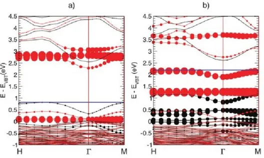
negatively charged, were calculated, at the level of DFT with on-site Coulomb interaction (DFT+U) description. They are reported in Figure 1.3. Black and red lines correspond to spin-up and spin-down states, respectively. Circles indicate d-Co contribution to the electronic levels, as circle radii are proportional to the integral of the corresponding charge densities projected on atom-centered orbitals. The horizontal blue line marks the position of the last occupied eigenvalue. In figure 1.3(a), empty levels induced by neutral Co–VO are resonant in the conduction band
(CB), about 0.5 eV higher than the CBM, while the zero of the energy scale is the VBM. In Fig. 1.3(b), the calculated Co-VO-induced electronic states get filled by