!
"#$%&'($)*!+&,-$!.)/+$!+$!.0-&'#1!
! ! "#$%&'#()*'+!,#!-*.).*)&#%!,)//0-*1+&(%2#+*)!),!-*.).*)&#%!3/)''%! ! "+''+&%'+!,#!5#4)&4%!#*!-*.).*)&#%!,)//0-*1+&(%2#+*)! 6-!7#4/+!8!9:+;%!<)&#)!! ! !=
3<-!"-!"
>==>5?=>!
!
2#0-3($(!0#+!4&($,#!15!!
678.$9!:$;1-0'!<1+&!!
=$&-+!>55&?)!@1A&'!B'0#($()1'!!
C:<=>BD!
!
7
?9"-"?=>@
!E
"FGF!4F
!:>H>4>BBI!
!
!
=
A=>5@
!!!!!
!!!!!!!!!@
JI=K
!.
2EL2BIJ>!:>EEIH>!
!
!
7
>>5"-9?=>53@
!!!!!@
JI=K
!2
HG>EI!<2J9>EEF!
!
Contents
Contents ... I List of Figures ... IV Acknowledgments ... VII Abstract ... VIII Thesis Outline ... XI Chapter 1 ...14H-SiC and Bipolar Mode Field Effect Transistor ...1
1.1 4H-SiC for High Power Transistors ...1
1.1.1 Unipolar devices ... 4 1.1.1.1 Schottky rectifyer ... 4 1.1.1.2 JFET ... 5 1.1.1.3 MOSFET ... 5 1.1.2 Bipolar devices ... 7 1.1.2.1 p-i-n rectifyers ... 7 1.1.2.2 BJT ... 8 1.1.2.3 IGBT ... 8 1.1.2.4 GTO ... 9 1.2 4H-SiC BMFET ... 9 1.2.1 Normally-off behavior ... 11 1.2.2 Conduction state ... 12 1.2.3 Switching ... 15 1.3 Conclusion ... 18 Chapter 2 ... 19
Potential Barrier Model ... 19
2.1 Motivation ... 19
2.2 Theory of the Potential Barrier Height Model ... 20
2.2.1 Zone I ... 23
2.2.2 Zone II ... 24
2.2.3 Zone III ... 25
2.2.3.1 1-D term of EM ... 27
2.2.3.2 Cylindrical terms of EM ... 27
2.3 Model Validation ... 34
Chapter 3 ... 45
Sub-threshold Drain Current Model ... 45
3.1 Motivation ... 45
3.2 Drain Current Model: Theory ... 46
3.3 Model Validation ... 47
3.3.1 Numerical simulation results ... 47
3.3.2 Experimental comparisons ... 53
Chapter 4 ... 55
Modeling of Reverse Recovery of 4H-SiC p-i-n Diode ... 55
4.1 Motivations ... 55
4.2 Switching-off Model ... 56
4.2.1 Storage ... 60
4.2.2 Turn-off ... 64
4.2.2.1 Carrier distribution ... 64
4.2.2.2 Transients of current and voltage ... 65
4.3 Model Validation ... 69
4.3.1 Numerical simulation comparisons ... 69
4.3.2 Experimental Comparisons ... 76
4.4 Circuit Representation of the Model ... 78
Chapter 5 ... 81
Hole Injection Efficiency of Implanted p+ Anode Regions ... 81
5.1 Motivations ... 81
5.2 Simulation of p+-n Junction: Hole Carrier Distribution and Forward J-V Curves ... 83
5.3 Hole Densities in Al+ Implanted Regions ... 87
Chapter 6 ... 91
BMFET Mask Design ... 91
6.1 Process Steps ... 91
Chapter 7 ... 97
V2O5 as Anode of a 4H-SiC Schottky Diode ... 97
7.1 Motivations ... 97
7.2 Device Fabrication ... 98
7.3 Results and Discussion ... 99
Conclusions ... 109
APPENDIX A ... 113
APPENDIX C ... 123
APPENDIX D ... 127
APPENDIX E ... 131
Related Pubblications ... 133
List of Figures
Fig.1.1.: Application of Silicon power devices... 2
Fig.1.2.: Cross section view of a Normally-Off VJFET structure ... 5
Fig.1.3.: Cross section view of DIMOSFET (a) and UMOSFET (b) structures ... 6
Fig.1.4.: Cross section view of a BJT structure ... 8
Fig.1.5.: Cross section view of a BMFET structure... 10
Fig.1.6.: JD and JG as function of VDS for different XCH values at VGS=0V. In the insert the circuit schematic is shown ... 11
Fig.1.7.: Gummel plot of BMFET with XCH=0.9!m at VDS=20V ... 12
Fig.1.8.: JD-VDS characteristics of BMFET with XCH=0.9!m at room temperature 13 Fig.1.9.: hFE-JD of BMFET with XCH=0.9!m at VDS=20V for different temperatures ... 14
Fig.1.10.: JD-VDS characteristics of BMFET with XCH=0.9!m at different temperatures ... 15
Fig.1.11.: 600V/100Acm−2 -inductive load a) output and b) input switching-on transients of a BMFET with XCH=0.7!m and YEPI=15!m. T=300K... 16
Fig.1.12.: 600V/100Acm−2 -inductive load a) output and b) input switching-off transients of a BMFET with XCH=0.7!m and YEPI=15!m. T=300K... 17
Fig.2.1.: Cross section of the p+ -n-p+ structure cell with the sketch of the hole carrier distribution at y=0 ... 21
Fig.2.2.: Comparisons between model and simulation of EX along the x-axis at y=0 in thermal equilibrium condition for XCH-1!m, YR-1!m and different YG structures ... 26
Fig.2.3.: Shape of a space charge region of gate, showing the cylindrical and planar component of the electric field ... 28
Fig.2.4.: Simulated 3D charts showing, for the half-cell of Fig.2.1, the variation of the electric field y-component and hole density, with respect to their equilibrium values, when a,b) VDS =10V and VGS=0V and c,d) VGS=2V and VDS=0V ... 29
Fig.2.5.: Cutaway view of the y-component of electric field at x=0 ... 31
Fig.2.6.: Comparisons between numerical simulations and model of VS/CH, VG/CH and VS/CH+VG/CH as function of XCH for the 4H-SiC structure in Table 2.1 at a) VGS=0V and b) VGS=2V ... 35
Fig.2.7.: Comparisons between model and numerical simulations a) VS/CH and b) pSP as function of XCH for the 4H-SiC structure in Table 2.1 for different values of YG and YR under equilibrium conditions ... 36
Fig.2.8.: Comparisons between model and numerical simulations VS/CH as function of XCH for the 4H-SiC JFET in Table 2.1 with YR=0.5µm for different values of YG and NEPI under equilibrium conditions ... 37
Fig.2.9.: Comparisons between model and numerical simulations a) VS/CH and b)
XCH=1µm, YR=0µm and different values of YG under equilibrium
conditions ... 38 Fig.2.10.: Model and numerical simulations comparisons of (a) VS/CH and (b) pSP as
function of XCH for the 4H-SiC structure in Table 2.1, using different VDS
with VGS=0V ... 39
Fig.2.11.: Model and numerical simulations comparisons of VS/CH, at VDS=10V, as
function of XCH for different YG of the 4H-SiC device in Table 2.1, by
using (a) YR=0µm and (b) YR=1µm ... 40
Fig.2.12.: Model and numerical simulations comparisons of VS/CH as function of NEPI
for the 4H-SiC structure in Table 2.1, using XCH=1µm and different VDS ...
... 41 Fig.2.13.: Model and numerical simulations comparisons of (a) VS/CH and (b) pSP as
function of XCH using different VDS and YG for the Si structure in Table 2.1
... 42 Fig.2.14.: Comparison between model and data [60] of the normalized potential
barrier, VS/CH/Vbi, as a function (a) of
2
EPI CH
N X product and (b) of the channel doping, NEPI ... 43
Fig.3.1.: Model and numerical simulations comparisons of the ID-VGS curves for
the 4H-SiC structure in Table 2.1 using (a) XCH=1!m with different YG
and VDS and (b) different XCH at VDS=1V (symbol) and VDS=10V
(symbol+cross) ... 50 Fig.3.2.: Model and numerical simulations comparisons of the ID-VGS curves, at
VDS=10V, using different XCH and YR for the 4H-SiC structure in Table 2.1
... 51 Fig.3.3.: Model and numerical simulations of ID-VGS curves for the Si structure in
Table 2.1, obtained using (a) different XCH and VDS and (b) XCH=0.5µm,
VDS=5V and different YG ... 52
Fig.3.4.: Model and measurement comparisons of SemiSouth Laboratory Inc. SJEP170R550 ID-VGS characteristics at VDS=10V and 20V... 53
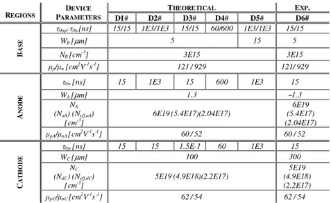
Fig.4.1.: a) Basic circuit used for numerical simulations and schematization of temporal-spatial hole profiles during the switching-off. Typical shape of the voltage b) and current c) transients ... 57 Fig.4.2.: Steady-state characteristics of all devices used in the analysis ... 70 Fig.4.3.: Current (a) and voltage (b) waveforms for diodes D1#, D2#, and D3# in Table 4.1, switched from JF =208A/cm2 with VEXT=−3V and
REXT=0.1"cm2 ... 71
Fig.4.4.: Current (a) and voltage (b) waveforms for diode D5# using different reverse voltages VEXT=−5V, −10V, −15V and fixed JF=64A/cm
2
and
REXT=0.1m"cm2... 72
Fig.4.5.: Current (a) and voltage (b) waveforms for diode D4# using different REXT
and fixed JF=1kA/cm 2
and VEXT=−10V. REXT value has been put equal to
13.5m"cm2
Fig.4.6.: Current (a) and voltage (b) waveforms and temporal variation of the space charge width (c) for diode D1# using different reverse current and fixed
JF=208A/cm 2
. Curve A: VEXT=−3V, REXT=10m"cm 2
; Curve B:
VEXT=−3V, REXT=0.1"cm 2
; Case C: VEXT=−10V, REXT=0.1"cm 2
... 74 Fig.4.7.: Comparisons of simulated voltage transients of D2# (Fig.4.3b), D5# (curve B in Fig.4.4b), D1# (Fig.4.3b) and D4# (curve B in Fig.4.5b) with the model using (4-27) for WSCR(t) calculation ... 75
Fig.4.8.: Transients of hole distribution (a), hole current density (b) and electric field (c) for diode D1# using JF=208A/cm2, REXT=0.1"cm2 and
VEXT=−3V ... 76
Fig.4.9.: Comparisons of (a) current and (b) voltage waveforms for diode D6#. Switching conditions: JF=59A/cm2, REXT=57m"cm2, VEXT=−40V ... 77
Fig.4.10.: Comparisons of current (a) and voltage (b) waveforms for diode D6# . Switching conditions: CurveA: JF=13.5A/cm
2
, REXT=200"cm 2
,
VEXT=−1V. Curve B: JF=8.8A/cm2, REXT=200"cm2, VEXT=−0.5V... 78
Fig.4.11.: Static and dynamic circuit schematic of a p-i-n diode... 79 Fig.5.1.: (a) Hole depth profile for different YEPI and ionized acceptor
concentration values of the Al+ implanted anode at a forward voltage of
4V. The vertical dashed line represents the metallurgical junction. (b) Effective doping concentration in the anode as function of ionized acceptor density (Ion. Doping) ... 84 Fig.5.2.: Simulated forward current-voltage characteristics of Al+
implanted 4H−SiC p-i-n diodes for different values of the activated acceptor concentration and of the n-type base thicknesses ... 85 Fig.5.3.: Comparison between model and numerical simulation results of the forward current-voltage characteristic for YEPI=25!m and
19 3
5 10
aA
N− x cm−
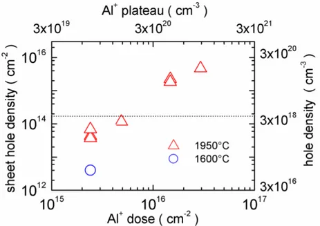
= ... 86 Fig.5.4.: Hole density in the Al+
implanted layers in terms of the Al implanted atoms for 1600°C/20min and 1950°C/5min. The horizontal dashed line corresponds to the majority concentration of 5x1018cm-3 ... 88 Fig.5.5.: Sheet resistance of the Al+ implanted layers after a 1950°C/5min annealing. Sheet resistance has been converted in the material resistivity by taking into account the thickness of the implanted layers (0.3!m) .... 89 Fig.6.1.: The six mask layouts for the lithography process steps ... 94 Fig.6.2.: Superposition of the first five mask layouts ... 95 Fig.7.1.: Comparisons of JD−VD curves of finite samples (S1), without HF-etch
with annealing (S2) as-deposited sample with HF-etch (S3) at T=298K. The cross-section of the structure is reported in the insert. ... 99 Fig.7.2.: Model and measurements comparison of the forward (a) and reverse (b)
JD−VD at T=298K. The insert in (a) shows the forward JD-VD curve using
Fig.7.3.: Comparisons between measurements and model results of 2
D C−
−VD curves
for a signal frequency of (a) 1kHz, (b) 10kHz, (c) 100kHz and (d) 1MHz. The signal amplitude is 100mV and T=298K.. ...104 Fig.7.4.: Forward (a) and reverse (b) JD−VD curves from T=100K to T=425K. The
step is 25K. ...106 Fig.7.5.: The barrier height (ΦBN) and ideality factor n vs. T. In the insert ΦBN vs. n is plotted. ...106 Fig.7.6.: (a) ln(IS/T
2
) vs. 103/T plot evaluated from the intercept of the forward diode characteristics of Fig. 7.4. (b) ln(IR/T
2
) vs. 103/T plot evaluated from the diode reverse currents for VD=−0.3V and −1V ...107
Fig.7.7.: Comparisons of JD−VD curves among V2O5/4H-SiC, IrO2/4H-SiC, Ni/4H−SiC and ideal (#BN=1eV) SBJs. ...108
Acknowledgments
Although it was very hard and difficult at the beginning of these three years, I had the opportunity to work side-by-side or, better,
pen-by-pen with one of the better experts in electron devices, from which I tried to absorb some of his boundless knowledge. What I learned cannot be substituted by other experiences. He was not a tutor, but more a master. Thanks You, Prof. Salvatore Bellone.
Along my course I met many people with which I discussed, compared, grew up. So, I would like to thank the people of my group and of Laboratory I7, Gian Domenico, Mario, Rosalba and Prof. Rubino, but also Prof. Della Corte, Dr. Roberta Nipoti and Dr. Michelina Festa. Moreover, all my colleagues of XI Ciclo and, in specially way, Dr. Giovanni Massa which has lost part of his time for my talk.
I would to thank my family.
... and to the only person who believed in me, supported me and knows the passion that I put into this work. My Love, Chiara.
Abstract
Analysis and design of a new 4H-SiC bipolar power transistor are the main topics of this Ph.D. thesis. The device is the Bipolar Mode Field Effect Transistor (BMFET) and exploits the electric field due to the channel punching-through in order to have a normally-off behavior and the minority carrier injection from the Gate regions to the channel in order to obtain the channel conductivity modulation. The structure of the transistor is oxide-free and its advantages are due to the lower conduction resistance, to the higher output current density and blocking voltage and to the elevated switching frequency, which make it competitive with commercial 4H-SiC JFETs or BJTs.
These activities, which have been completed with the definition of the main process steps and of the mask layouts, are supported by a technology activity and by an intense modeling activity of BMFET electrical characteristics, which has been validated by comparisons with the results of numerical simulator (ATLAS Silvaco) and the measures of commercial devices having a similar structure, like Vertical Junction Field Effect Transistors.
In the former activity, in order to obtain an integrated free-wheeling diode in antiparallel configuration to BMFET, an original 4H-SiC Schottky rectifier has been fabricated; precisely, for the first time in the literature, DiVanadium PentOxide (V2O5), a Transition Metal Oxide, has been used as anode contact of the rectifier. The device is a heterojunction between a thin V2O5 layer, which is thermally evaporated and has a thickness of around 5nm, and a 4H-SiC n-type low doped epilayer. By analyzing the JD-VD and CD-VD curves, the structure has a rectifier behavior with a high/low current ratio higher than seven order of magnitude and its transport mechanism is described by the thermoionic emission theory characterized by a Schottky barrier height and an ideality factor
between 0.78eV and 0.85eV and between 1.025 and 1.06, respectively, at room temperature.
Because the gate doping concentration greatly influences the BMFET performances, as input resistance, DC current gain and blocking voltage, Aluminum ion implantation process, used to realize the Gate regions, is strongly analyzed in terms of the dose concentrations and of the annealing temperature. It will show as the necessity of a low BMFET on-resistance, which is possible with highly conductive gate regions in order to permit high injection levels of the minority carriers, is counteracted by the Aluminum incomplete ionization in 4H-SiC. This phenomenon together with the band-gap narrowing effect limits the hole carrier density from gate to channel. The analysis, in collaboration with the Institute for the Microelectronics and Microsystems (IMM) of CNR in Bologna, Italy, consists to reveal the effects of various different doses at different temperature annealing (1920K and 2170K) on the gate injection efficiency and on the input current density.
Since the introduction of the first normally-off Si JFET in ‘80 years, the description of the potential barrier height into the channel has been unresolved due to the complex relations with the channel geometry and bias conditions. In the second activity an analytical model of the potential barrier height in the channel is proposed and compared with the numerical simulation results by changing the channel length and width, respectively in the range 0.1÷6!m e
0.5÷3!m, the channel doping concentration, between 1014
÷1017cm-3, and the output and input bias voltages. Moreover, it has been also validated by using Silicon as semiconductor material, permitting to extend it to other devices with similar structures, like BSITs, VJFETs and SITs. From this model the trans-characteristics of the transistor in sub-threshold condition and in unipolar conduction is developed and its validity is verified comparing its results with numerical simulations and experimental data.
Finally, the analysis of the input diode during the switching-off has been performed because the switching capability of the BMFET depends on the storage charge into the channel during the “on” state. The result is the development of an analytical model that describes the spatial distributions of the electric field, of the minority carrier
concentration and of the carrier current densities into the epilayer at each instant during the switching, in addition obviously to the current and voltage transients. It is shown as the combination of this model with another static model just developed in a previous Ph.D. thesis is an useful instrument to understand how physical parameters, which are dependent on the manufacturing processes, as carrier life-time and doping concentrations, can affect the dynamic behavior.
Thesis Outline
After a brief introduction on the state-of-art of the 4H-SiC power devices, in Chapter 1 BMFET operating principle is shown with the motivations and the interests in this kind of transistor.
Chapter 2 is dedicated to the analysis of the channel potential barrier and to the comparisons between the results of the proposed model and of the numerical simulator for numerous values of the physical and geometrical channel parameters and of voltage bias conditions.
The model of ID-VG characteristics in sub-threshold condition have been developed from the previous model and shown in Chapter 3. Its accuracy to predict the electrical behaviour of simulated and commercial structures is reported.
From the analysis of the switching performances the influence of the intrinsic p-i-n diode is highlighted and in Chapter 4 the dynamic model of the reverse recovery of the diode is shown.
Chapter 5 covers on the results of the analysis of the Aluminium ion implantation doses which can affects the performances both of the BMFET due to the Gate injection efficiency and of the maximum
p−i−n diode current density.
The mask layouts and the mainly process steps to realize a BMFET transistors are described in Chapter 6.
Finally, in Chapter 7 the fabrication process and the experimental results of the free-wheeling V2O5 diode in are reported. Diode current−voltage and capacitance−voltage curves have been used to extract the main physical parameters of the Schottky Barrier Junction, i.e. barrier high, ideality factor and serie resistance. The measurements have been performed in a temperature range between 100K and 425K.
Chapter 1
4H-SiC and Bipolar Mode Field Effect
Transistor
In this chapter an overview of 4H-SiC power transistors and of its main physical parameters precedes the description of the operating principles of Bipolar Mode Field Effect Transistor (BMFET) in order to highlight the motivations and advantages of this kind of device. Results of numerical simulation are used as instruments of investigations.
1.1
4H-SiC for High Power Transistors
Silicon technology has always dominated the power electronic in terms of semiconductor devices, which are able to operate in a broad spectrum of power levels and frequencies. Two-terminals devices, like
p-i-n and Schottky Rectifiers, and three-terminals devices, like Gate Turn-Off (GTO) Thyristors or Bipolar Junction (BJT), Insulated-Gate Bipolar (IGBT) and Field Effect (FET) Transistors, exist. Each of them has its own field of application ranging from communications to power transmissions as identified by the capability of managing power and frequency of operation as shown in Fig.1.1, including variable speed motion control, electric vehicle drives, uninterruptible power supplies (UPS), up to the high power distribution, transmission and traction markets. However, the need for devices with higher switching
frequency, high voltage capability and small area is growing, especially, for military and advanced power conversion. Additionally, the intrinsic physical properties of Silicon limits the operating junction temperature to 423K and it means the mandatory employment of cooling system, which increases the cost and the circuit area, and the difficulty to satisfy the require performances in harsh environments.
Therefore, it needs to consider other semiconductors with better performances respect to Silicon in terms of critical electric field (EC), saturation velocity (vSAT) and thermal conductivity ($). These are the wide band-gap semiconductors, in particular Gallium Nitride (GaN) and Silicon Carbide (SiC), whose most relevant physical parameters are compared in Table 1.1.
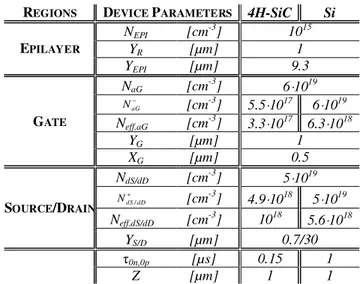
PARAMETERS UNITS Si 3C-SiC 4H-SiC 6H-SiC GaN
εR 11.9 9.72 9.66 9.66 8.9 % [eV] 4.05 - 3.7 3.4 4.1 300 K G E ° [eV] 1.1 2.36 3.26 3 3.39 EC [MV/cm] 0.3 ~1 3÷5 3÷5 ~5 vSAT [x107cm/s] 1 2 2.2 1.9 2.6 16 3 10 n N cm µ = − [cm2V-1s-1] 1500 !800 !900 !400 !1000 16 3 10 p N cm µ = − [cm 2V-1s-1] 480 !320 !120 !90 !200 $ [Wcm-1K-1] 1.5 3.2 3.7 3.6 1.3
Table1.1. Electrical parameters of some wide band-gap materials compared with Si [1], [2]. Fig.1.1. Application of Silicon power devices.
With respect to Silicon, the higher critical electric field of wide band-gap semiconductors can lead to power devices with higher breakdown voltages, or, for the same breakdown voltage, too much thinner drift layer that, in conjunction with the high vSAT, reduces the storage charged and, hence, the delay intervals increasing the switching frequency of devices. Considering also the higher thermal conductivity in the case of 4H-SiC, SiC devices operate at very high temperatures and high-medium power densities at medium-high frequency switching applications [3]−[4]. Moreover, SiC dissemination has been favored: i) by fabrication processes very similar to Si, being SiC the only wide band-gap semiconductor with a native oxide (SiO2); ii) by the availability of high-purity commercial wafers [5]; iii) by the continuous technology improvement from the epitaxial growth to the ion implantation processes.
Depending on the stacking order of the Silicon and Carbon atoms, over 200 crystal structures exist, which are called polytype, but a few of them are reproducible in laboratory, stable and with interesting physical properties for electronic applications: they are 3C−SiC, 6H−SiC and 4H−SiC (see Tab. 1.1). If 3C−SiC wafers suffer of low quality of the substrate, 6H−SiC and 4H−SiC wafers are commercially available, but the last has a higher carrier mobility, which is preferred to reduce the conduction losses.
In order to design new devices by using new semiconductor, the role of numerical device simulators is fundamental and, although the same general equations used for modeling conventional semiconductors can be applied to wide band−gap, a number of peculiar phenomena, having a marginal influence on Si device operations, must be accounted for. In particular, effects like incomplete ionization of doping atoms, band-gap narrowing, mobility along with their temperature and doping dependences must be accurately modeled. In this thesis each of these phenomena with the relative physic model are accurately considered and recapitulated in APPENDIX A.
In spite of the favorable aspects, at present, 4H−SiC is employed in a reduced number of commercial power devices, like Schottky diodes, FETs and BJTs. Schottky diodes are commercially available for the rectifiers market, reaching maximum voltage and current of
1200V and 40A [5]−[8], while state-of-the-art of MOSFETs [5], JFETs [9] and BJTs [10] are capable to manage blocking voltage between 1200V and 1700V and forward current up to 100A. The capability to realize a gate oxide of good quality has defined the success of MOSFETs as the main power transistor in Si technology due to the high input impedance, which simplifies the design of the control circuits. For this reason, it seems to be the most promising device, but the scarce quality of the SiO2/SiC interface limits its large diffusion. Although JFETs and BJTs are commercially available, they are still under study in order to improve both the technology and the performances, which are superior for high power applications, thanks to the lower forward voltage drop and higher blocking voltages than Silicon counterparts.
This scenario gives an idea of the excitement around SiC that involves both industries and research institutes. In the following, the main 4H-SiC power devices are shown.
1.1.1
Unipolar devices
Unipolar devices have been the first topology developed and commercialized in 4H−SiC. They are Schottky rectifiers and FETs family: MOSFETs and JFETs.
1.1.1.1 Schottky rectifiers
Schottky Barrier Diodes are metal-semiconductor junctions and the diode current-voltage dependency is due to the potential barrier at the interface. By choosing the metal with the appropriate work function, a low forward voltage is allowed by lowering the potential barrier. Otherwise, a reduced potential barrier determines a higher leakage current and, hence, a lower blocking voltage. A trade-off between the conduction losses and the reverse conditions is required [11], especially at high temperature conditions. Due to the absence of the minority carriers, the switching off is defined by the space charge capacitance, proposing these devices for high frequency applications. Being the first 4H−SiC device commercially available, maximum voltage and current are 1200V and 40A [5]−[8], respectively.
1.1.1.2 JFET
The first proposed commercial transistor is the unipolar Junction Field Effect Transistor from SemiSouth Laboratories Inc. [9], whose investigation shows good blocking and dynamics behaviors [12]−[14], but the typical problems of an unipolar transistor, which concern high
RON and low current density comparing with those of the bipolar family, currently stay. In Fig.1.2 the cross-section view of a Vertical channel-JFET is reported and, depending on the channel width, normally-on or normally-off behavior are possible due to the channel pinched-off at zero bias condition. This topology does not use gate oxide avoiding problems from oxide reliability and mobility reduction by interface states, which makes VJFET interesting also for high temperature applications. Although JFETs with interesting performances have been developed (VBL=1700V, RON=2.77m"cm2 [15] and VBL=1900V, RON=2.8m"cm2 [14]), the capability to reach very high blocking voltage is limited by the conduction losses that increase with it due to the unipolar conduction, as for example the device in [13] has VBL=11kV and RON=130m"cm2.
1.1.1.3 MOSFET
Thanks to the SiO2 formation, MOSFETs have been developed in 4H−SiC in different topology [16], which can be summarized in
Double Implantation MOSFET Fig 1.3a and UMOSFET Fig 1.3b. Both of them suffer of: i) premature failures at high reverse voltages, due to the high electric field at the oxide interface; ii) the injection of hot carriers into the oxide due to the smaller band offset among the conduction bands of the two materials; iii) the scarce quality of the interface, which induces a weak control of the channel mobility and of the threshold voltage.
DIMOSFET is realized by a Double Implantation for the p-well and n+-source regions and, then, by an oxide formation for the gate. This structure is planar and easily realizable, but is also limited, in addition to the aforementioned problems, by the reach-through problem into the p-well region, which limits the blocking voltage capability.
The second structure is realized by trenching the p−well and
n+−source epilayers with a U-shaped and by growing a native oxide for the gate oxide. Although its specific on-resistance is lower than DIMOSFETs, its limitation is due to the extremely high electric field at the corners of the trench, that causes a poor long term reliability.
Until now, DIMOSFETs with VBL=1.2kV and RON=9m"cm2 [17] have been developed as well as UMOSFETs with VBL=1.4kV and
RON=15.7m"cm2 [18], but, like JFETs, it is needed a tread-off between conduction loss and blocking voltage as shown in [19] where a 10kV-class DMOSFET has a ON-specific resistance of 123m"cm2.
1.1.2
Bipolar devices
Bipolar devices are interesting for high voltage applications due to the conductivity modulation phenomena, which permits to have a thick and low-doped drift layer, in order to support high blocking voltages in the range of 10kV, with very low ON-specific resistances, less than
100m"cm2
. Naturally, the injection of the minority carriers needs a maintenance input current during the on-state, making complex the gate driver circuit, and the injected carriers into the drift layer have to be extracted during the switch-off of the device, causing a poor dynamic performance.
1.1.2.1 p-i-n rectifiers
p-i-n power diode is a vertical structure in which two high doped p+ (anode) and n+ (cathode) regions are divided by a high resistive n-type layer. In reverse bias the voltage mainly drops in the intermediate region, indeed, in forward conditions the ON-resistance of the drift region is lowered by the minority carriers injection from the anode. The former is known as punch-through configuration, indeed, the second is the modulation conductivity phenomena, which is peculiar to the bipolar devices. Otherwise, p-i-n diode operates at low switching frequency due to the slow reverse recovery, which is necessary to remove the stored carrier from the drift layer, and shows a high forward overvoltage during the switch-on due to the low doping concentration of the i-region.
Thank to the higher critical electric field, 4H-SiC p-i-n diodes have drift region with higher doping concentration and thinner thickness than Si counterparts, improving dynamic and static performances, in addition to operate at higher temperature. Although high-voltage 4H-SiC p-i-n diodes have been fabricated having blocking voltages of 6.5kV [20] or 10kV [21] and RON=34m"cm2 at
JD=100A/cm2, their performances are degraded by the nucleation of the Schockley Stacking Faults from the basal plane dislocations in the substrate during forward bias stress [22]. This phenomena is known as bipolar degradation and consists in a reduction of the carrier life-time
and/or in an increasing of the forward diode voltage drop due to the creation of recombination centers.
1.1.2.2 BJT
Typical silicon BJTs architectures are not easily realized in SiC, mainly due to the lacking of a reliable technology for the activation of acceptor species. On the other side, if the doping of p-type base region were done by implantation, the lifetime of the carriers would be very low, giving rise to a decrease in the obtainable current gain. To avoid these drawbacks, the architecture of bipolar transistors proposed in the literature relies on multiple epitaxial layers [23]-[25] as in Fig. 1.4, but it presents high manufacturing costs.
Actually, BJTs have been developed with VBL=1.2kV,
RON=5.2m"cm2 and hFE=60 [26], VBL=2.8kV, RON=4.5m"cm2 and
hFE=55 [27], VBL=9.2kV, RON=33m"cm2 and hFE=7 [28]. !
!
1.1.2.3 IGBT
Insulated Gate Bipolar Transistor combines the low forward voltage drop due to the conductivity modulation, which places it among bipolar devices, with the high input impedance of the voltage controlled MOSFET. It has been classified in the bipolar devices and is limited by high switching losses due to the extraction of the minority carriers from the drift layer. Because the process to obtain a low interface state density is actually better for n-MOSFET, n-channel IGBT is the preferred to the p-channel IGBT, but it needs of a
high−quality p-type substrate which is not available in large diameter and high doping concentration. In [29] n-IGBT shows VBL=13kV and
RON=22m"cm2.
1.1.2.4 GTO
Gate Turn-Off thyristors permits to reduce the turn-off time by reversing the gate drive current at the expense of large current tails, limiting its use to high power DC applications. The possibility to realize a 4H-SiC GTO leads to manage very high blocking voltages at higher junction temperatures [30].
1.2
4H-SiC BMFET
Bipolar Mode Field Effect Transistor (BMFET) combines the normally-off behavior of a Vertical JFET with the conductivity modulation of a bipolar transistor. Briefly, the operating principle is based on the superposition of the Space Charge Regions, SCRs, formed by p-n junctions, which induce a potential barrier in the channel blocking electron flow from source to drain when the transistor is in OFF state; during the conduction mode, instead, hole carriers are injected in the channel from gates in order that the output resistance reduces for the conductivity modulation effect.
Device structure is reported in Fig. 1.5, where XCH represents the channel width coincident with the gate-to-gate distance and YG is the depth of gate placed YR away from the bottom of source. Although it is similar to a VJFET structure (Fig.1.2), epilayer doping concentration,
NEPI, is less than the typical VJFET value of 1016cm−3 [14] in order to have a high potential barrier height, VS/CH, with shallow junctions, since doping thermal diffusion coefficients are negligible under
1800°C [31]. Potential barrier dependency on the geometric and physic parameters is analyzed in detail in the next chapters.
The following BMFET electrical characteristics have been obtained by numerical simulations [32] for a similar structure to that in Fig. 1.5, whose geometrical and physical parameters are reported in Tab. 1.2; the implemented physical models are in APPENDIX A. It is worth to note that, since ion-implantation is the most critical device
process, gate region parameters are related to Al ion-implanted p-n junctions analyzed in Chapter 4 and 5.
REGIONS DEVICE PARAMETERS 4H-SiC
EPILAYER NEPI [cm-3] 1015 XCH [µm] 0.9 YR [µm] 1 YCH = YR +YG [µm] 2 YEPI [µm] 10 GATE NaG [cm-3] 6⋅1019 aG N− [cm-3] 5.5⋅1017 Neff,aG [cm-3] 3.3⋅1017 YG [µm] 1 SOURCE/DRAIN NdS/dD [cm-3] 1019 / dS dD N+ [cm-3] 2⋅1018 Neff,dS/eff,dD [cm-3] 6.6⋅1017 YS/D [µm] 0.7/30 Rn+ ["cm2] 10−4 Rp+ ["cm2] 10−5 &0n,0p [ns] 150 Z [µm] 1
Table1.2. Main physical and geometrical parameters of the structure in Fig.1.5. Fig.1.5. Cross section view of a BMFET structure.
1.2.1
Normally-off behavior
Depending on the channel geometry and doping concentration both normally-on and normally-off behaviors are allowed. Let us consider a BMFET structure of Tab.1.2 and the circuit schematic in the insert of Fig. 1.6, where source and gate terminals are to ground and a forward drain−source voltage, VDS, is applied; the blocking voltage is defined as VDS value for which drain current densities, JD, reaches a maximum allowed value, which is 100!A/cm2 in our case. In Fig. 1.6, for wide channel (XCH=1.2!m), the maximum JD value is reached at Vbl=364V when the gate current density, JG, is still low meaning that the channel opens due to the decreasing of the potential barrier; instead, by reducing the channel width, the blocking voltage increases (Vbl=860V) with VS/CH in the case of XCH=1!m, until to detect the gate-drain diode breakdown at XCH=0.9!m with Vbl=1257V.
Fig.1.6. JD and JG as function of VDS for different XCH values at VGS=0V. In the insert
1.2.2
Conduction state
In Fig. 1.7 Gummel plot is reported for a BMFET structure of Tab.1.2 at VDS=20V. JG−VGS characteristics is typical of a p-n junction, which is in medium and high hole injection regime for
VGS>2VTln(NEPI/ni)'2.6V; over this voltage, channel conductivity modulation is obtained as shown to the further increasing of JD between 102 and 103A/cm2. About the lower part of the output current, the exponential behavior is due to the modulation of the potential barrier height by applying VGS. It is known as sub-threshold region and will be addresses in Chapter 3.
Output characteristics are reported in Fig. 1.8 and, for hFE,forced=12 and
JD=100A/cm2, VDS,SAT is 0.35V in the saturation region that means an on-resistance of 3.5m"cm2, which is much lower than the intrinsic on-resistance [16]:
, 1 1 ln 1 2 0.5 CH G CH G ON Unipolar n EPI CH CH CH EPI CH CH CH CH G Y X X X r q N X Y X Y X X Y X X µ ! " # " # = % + &$ + % + &+ ' () ' ( * − + + + , (1.1)
equal to 8.2m"cm2. This is due to the conductivity modulation appearing when hole carriers are injected in the channel once p-n junction is forward biases. Moreover, the ratio between JD and JG defines the common source current gain, hFE, and is reported in Fig. 1.9 for the same structure and electrical condition of the previous device; hFE values of 86 and 44 are at JD equal to 355A/cm2 and
585A/cm2, respectively.
Each single cell is connected in parallel on the same die in order to achieve the desiderated output current and, therefore, a thermal stability have to be reached to avoided thermal runaway, which can destroy the device. This thermal property is shown in Fig.1.9 for a temperature range of 300÷523K and, similarly to 4H-SiC BJTs [33], is the results of combined temperature dependences of carriers lifetime and ionized dopant density, whose impurity energy levels have been set 190meV and 70meV (see APPENDIX A) for acceptor and donor, respectively. Moreover, in Fig. 1.10 the thermal stability of BMFETs is confirmed also in the saturation region, where rDS,ON increase with temperature originates from decrease of the electron mobility in the drift region contrasting the thermal runaway.
1.2.3
Switching
In Fig. 1.11 and 1.12 input and output transients are reported for BMFET driving a clamped inductive load during the switching on and off, respectively. The inductive load has been modeled with a constant current source and an ideal diode in series with a voltage source, as in the insert of Fig. 1.11.b. When BMFET is in OFF-state, the load current, ILOAD, imposed by the ideal current source, flows through the free−wheeling diode and the high external voltage, VDC, drops across the device, then, when BMFET is in ON−state, the input voltage source with a series resistance applies gate current in order that BMFET is in saturation region and the low drain voltage is able to turn off the diode absorbing ILOAD. This last has been chosen equal to
100A/cm2 and the clamping voltage is 600V, which are typical values assumed to test a medium-high power transistor. Moreover, the bias conditions are to have a hFE,forced of 8.5 and a VDS,SAT of 0.39V. The device structure is the same of Table 1.2 with XCH=0.7!m and YEPI=15
!m.
During the switching on, a voltage step is applied to the gate as
Fig.1.10. JD-VDS characteristics of BMFET with XCH=0.9!m at different
reported in Fig. 1.11 and IG instantly increases, showing a spike due to the input capacitance. After a delay time, tD, of 0.63ns, at first ID sharply reaches its ON−state value, while VDS softly falls to VDS,SAT in
4.8ns owing to the charging of the gate−drain capacitance and to the injection of the hole carriers. Overall, the ON transient stands 5.7ns,
tON, and the ON switching energy, EON, is 0.19mJ/cm2.
Like all bipolar device, during the turning off the injected minority carriers have to be extracted and it is evident that the OFF time, tOFF, which is equal to 34.8ns, corresponds largely to the reverse recovery. Although tOFF is longer than tON, VDS sharply rises to the clamped voltage (trV~6.2ns) at the end of the storage and, once this condition is reached, IDS instantly falls to the leakage value. This drain current behavior is a peculiarity of BMFET because, differently from BJT in
Fig.1.11. 600V/100Acm−2-inductive load a) output and b) input switching-on transients of a BMFET with XCH=0.7!m and YEPI=15!m. T=300K.
which the current fall is due to the extraction of the remaining electron carriers stored into the base [34], once VDS reaches the clamping voltage, the formation of the barrier in the BMFET forces the removal of holes from gate and electrons from source. The disappearance of the current tail permits to have low energy loss during turning-off,
EOFF, which in this case is 0.18mJ/cm2.
It is worth to note that, due to the high drain-gate current ratio, both ON and OFF input switching energy are three order of magnitude lower than those of the output, having the input and output conduction power losses PCond equal to 33W/cm2 and 40W/cm2, respectively.
Fig.1.12. 600V/100Acm−2-inductive load a) output and b) input switching-off transients of a BMFET with XCH=0.7!m and YEPI=15!m. T=300K.
1.3
Conclusion
After a brief introduction on the fields of applications of 4H-SiC power device and on the state-of-art of available transistors, Bipolar Mode Field Effect Transistor structure is shown and main physical principles are described by using electrical characteristics. From this analysis three aspects are relevant:
• Potential barrier height dependency on geometrical and physical device parameters, which plays both in the OFF-state and in sub-threshold regime;
• Extraction of injected hole carriers during the storage time of switching-off;
• Hole injection efficiency of the p-type gate region, which is necessary for the channel modulation conductivity.
They are deeply addresses in the Chapters 2-3, 4 and 5, respectively. Moreover, being essential the presence of an integrated freewheeling diode in anti-parallel to BMFET, a Schottky diode is proposed in Chapter 7 by using an innovative material as anode contact, which is PentOxide DiVanadium (V2O5).
Chapter 2
Potential Barrier Model
The main topics of this thesis is on the development of a model which can describe the potential barrier height into the channel of a vertical structure, like BMFET, VJFET and BSIT, for any physical, geometric and electric configurations. That permits both to understand the physics behind the operation of this topology of transistors and to have an instrument to design the channel of the transistor.
2.1
Motivation
Since the introduction of Static Induction Transistor (SIT) in the early 1970s [35], which first demonstrated the feasibility of short depleted channel to realize normally-off behaviour JFETs, the effectiveness of the gate topology is become an important issue for controlling the output current of other JFET-like transistors, as BSIT [36] and BMFET [37], rectifiers [38], [39] and, more recently, Silicon Carbide JFETs [9], [40], [41] and BSITs [42]. Basically, the current controlling mechanism in these devices can be explained by observing that, as the channel width is reduced, the space charge regions of the two lateral gates overlap underneath the source by inducing in this way a voltage barrier which opposes to the electron injection from the source and increases the minority carrier density in the channel. Due to the complexity of the problem, design rules has been analyzed so far only by numerical methods to obtain the two-dimensional potential and carrier distributions within the channel [43]-[46]. Considering the proposed analytical models [36], [47]-[50], the solution derived in [36], [47]-[49] for the two-dimensional potential distribution are quite
inadequate for the assumption of a fully depleted channel, while the model proposed for the potential barrier in [50] using the Doping-Voltage Transformation [51]-[52] has been demonstrated valid only for a well defined BMFET structure. It must be observed that the absence of models describing the barrier height and free carriers concentration in the channel of BSITs for an arbitrary channel geometry and bias condition nullifies the effectiveness of numerous analytical models [48], [49], [53]-[55] published to describe the transfer characteristics of BSITs, stimulated probably from the similarity of the depletion regions overlapping and the holes accumulation, respectively, with the punch-through phenomenon of BJTs [56] and the inversion mechanism of MOSFETs. In fact, some of them [48],[49] support a description of the barrier height as function of the channel geometry and the applied voltage using a depleted channel approximation, the others [53]-[55] give analytical expressions of the output current which include, however, quantities achievable only by numerical simulations. Therefore, as follows from the above observations, the electrical behaviour of BSITs structures, represented by their input, output and transfer characteristics, still waits to be adequately modelled.
2.2
Theory of the Potential Barrier Height
Model
In order to extend the validity of this model to recessed-gate JFETs topologies, the channel geometry used in our analysis has been chosen as in Fig. 2.1, where XCH represents the channel width coincident with the gate-to-gate distance and YG is the depth of gate placed YR away from the bottom of source.
Moreover, to avoid the numerical integration of the two-dimensional Poisson equation for the need of including the mobile carriers, the analytical solution has been obtained by evaluating the gate-channel voltage VG/CH as the sum of the voltage drops across the three subzones encountered from the p+ region to the saddle point at the center (0,0), namely:
/
G CH I II III
V =V +V +V (2.1) With the help of the carrier profile sketched in Fig. 2.1, the zone I represents the gate region where the hole density varies from the ionized doping value, NaG− , to the unknown holes value pJ at the metallurgical interface, the zone II corresponds to the channel region closer to the interface with an holes density much higher than the epilayer doping, namely p x( )≥N*!NEPI, and, finally, the zone III represents the region where the hole density is comparable with
Fig.2.1Cross section of the p+-n-p+ structure cell with the sketch of the hole carrier distribution at y=0.
doping and disappears when the hole density at the saddle point, pSP, is greater than N*. It should be emphasized that, once VG/CH has been evaluated, the height of the source-channel barrier VS/CH can be obtained as follows:
/ /
S CH bi n n G CH
V =V +V+ −V (2.2)
being Vbi=VTln
(
Neff aG, NEPI ni2)
the built-voltage of the gate-channel diode, Vn n+ =VTln(
Neff dS, NEPI)
the built-voltage of the high-lowsource-channel junction, VT the thermal voltage, Neff,aG(dS) the effective gate (source) doping and ni the intrinsic concentration.
In deriving the model, these zones will be treated with the following assumptions:
a) after demonstrating that VI differs of a few millivolts from VT, it is taken, for simplicity, equal to the thermal voltage, VT, so that the unknown holes value at the metallurgical interface can be put equal to pJ =Neff aG, e−1;
b) the zone II coincides with the channel portion where the hole density, starting from pJ, remains greater or at least equal to
N*=20NEPI, to which its maximum width W* occurs;
c) the carrier transport in the zone III is governed by the drift and diffusion mechanism and the electric field varies likely a depleted region, namely:
(
*)
2 ( , ) 2 X M CH x E x y E X W = − (2.3)where EM is the maximum value at the border between the zones II and III and depends on both channel width and channel depth.
2.2.1
Zone I
Let considers the Poisson equation in gate region, only for the majority carriers and ions concentrations:
2 2 pF i T V i aG i d q N n e dx φ ψ ψ ε − − ! " # $ = − # $ % &
where !pF and "i are the hole quasi-Fermi and the electrostatic potential, respectively; integrating in [−#,−XCH/2], one obtains:
2 2 2 1 I T CH V V T aG I X T qV N V E e V ε − − − − ! " = ## − + $$ % & (2.4)
being VI is measured respect to VI(-#)=0. Analogously, if the Poisson equation is integrated in the region II assuming E(0)=0 for symmetry, the electric field at x=−XCH/2 can be written as follows:
2 2 2 1 II T CH V V T SP X qV p E e ε + − ! " = ## − $$ % & (2.5) Therefore, by expressing the total voltage VI+VII in terms of the apparent bandgap narrowing, $VaG, namely:
ln 2 aG aG I II T SP V V V N V p − ! " ∆ + = # $− % & (2.6)
and by imposing the equality of (2.4) and (2.5), one obtains:
2 1 1 aG I T T V V V V SP I T aG p V e e V N ∆ − − − ! " + ## − $$= − % & (2.7)
which can be numerically solved to obtain VIfor an arbitrary pSP. It is clearly from (2.7) that VI is at most even to VT, justifying the assumption a) in the previous section.
2.2.2
Zone II
For the assumption b) it is convenient to refer to a sufficiently small channel XCH in order to vanish the zone III and the thickness Wof the zone II coinciding with XCH/2. In this case, by neglecting the doping and electrons in Poisson equation, this latter can be written along the
x-direction as follows: 2 2 F i T V i i d q n e dx ψ ψ ψ ε − = − (2.8)
where !F and !i are the Fermi and the electrostatic potential in the channel, respectively. By integrating (2.8) in the interval [−XCH/2,0] and using as boundary condition the symmetry of the potential distribution along the channel,
0 0 i x d dx ψ = =
the electric field can be written as:
( )0 ( ) 2 ( ) 1 i i T x V T i qV pSP d E x e dx ψ ψ ψ ε − = − = − !## − "$$ % &
which, further integrated, yields:
8 1 tan J 1 T CH SP SP p V X qp p ε − ! " = ## − $$ % & (2.9)
This last can be iteratively solved to obtain for a given XCH the carrier density pSP and the voltage drop across the zone II:
ln J II T SP p V V p ! " = # $ % & (2.10) as long as pSP!N*. It is evident that, when XCH is wide enough to make
pSP<N*, i.e. XCH>2W*, (2.9) gives the maximum extension of the zone
II, namely: * * * 2 1 tan J 1 T p V W qN N ε − ! " = ## − $$ % & (2.11) and the voltage component VII is even to:
* ln J II T p V V N ! " = # $ % & (2.12)
2.2.3
Zone III
By considering the x-component hole current density negligible and by using the electric field (2.3), one obtains:
(
*)
2 2 M T CH E x dp dx p =V X − Wwhich, integrated in the interval [−(XCH/2−W*),0] with N* as boundary condition, yields the hole carrier concentration at the saddle point:
(
2 *)
4 * M CH T E X W V SP p N e − − = (2.13)(
*)
2 4 M III CH E V = X − W (2.14)By recalling that (2.3) has been derived assuming one-dimensional the electric field along the symmetry axis of gates, that is certainly true for gates infinitely deep (YG=!) and distant from the source
(YR=!), it obvious that the maximum electric field EM must be adequately written to incorporate the effects of finite YGand YR, whose reduction leads the electric field internally to the channel to be more influenced from that of gate corners and n+-n junction, respectively. Therefore, the maximum electric field is determined from the sum of a one-dimensional electric field and of the cylindrical contribution from the gate corners:
1 D CYL
M
E =E− +E (2.15)
In Fig.2.2 the EX distribution, evaluated from the model along the x-axis and y=0, is compared with the numerical simulation results for
XCH−1µ m, YR−1µ m and different YG structures in thermal equilibrium conditions. It is clear that the distribution is linear according to (2.3) and, as expected, by reducing the junction depth the maximum at the border between the zone III and II increases due to a major interaction among the electric fields at the gate corners.
Fig.2.2 Comparisons between model and simulation of EX along the x-axis at y=0 in
2.2.3.1 1-D term of EM
To properly account for the XCH effect on the JFETs conduction, as it will be shown in Chapter 3, it is necessary consider both fixed and mobile charges in Poisson equation along the x-axis; in fact, as
XCH increases, the electron density at the channel centre increases towards its neutral value, becoming inadequate the assumption of fully depletion. By integrating the Poisson equation with the condition
E(x)|x=0=0, one obtains:
1 2 1 1 III III T T V V V V D T EPI III SP SP t EPI EPI n p qV N V E e e V N N ε − − ! # $ # $" = % + '' − ((+ '' − ((& % ) * ) *& + ,
For the pursuit of simplicity, the contribution of hole carriers can be neglected since it become relevant for XCH!2W*, hence, it is accounted for by VII, indeed, the contribution of the electron carriers is relevant for VIII>>VT, so that, the first term in (2.3) can be rewritten as:
1D 2qNEPIVIII E ε − = (2.16) 2.2.3.2 Cylindrical term of EM • VDS=0V
Since EM in (2.14) represents the maximum field at the extremity of zone III, namely at (−XCH/2+W*), as shown in Fig.2.3, a convenient way to account for the field effects of the corners lies in assimilating the gate geometry to a cylindrical shape with radius rJ = L2d +YG2,
where the Debye length 1 1
2
d T EPI
L εV q N− −
= has been introduced to take into account the zone II when YG becomes infinitesimal. Therefore, assuming that the cylindrical shape extends at the same way of the parallel-plane behavior of the horizontal gate sides, it can be written as follows:
(
)
2 2 ( ) 2 2 G V SC j CYL j j W r qN E r rε
− = (2.15) where VG 2 1 1(
)
SCR EPI bi GS Wε
q N− − V V= − is the p+-n Space Charge Region
dependent on Gate-Source voltage, the further factor of two added to denominator arises from the symmetry of electric field due to the double gates [57] and N represents an equivalent channel doping dependent on YR. In fact, by noting that the abrupt change of the n-n+ junction doping modifies the electric field at the gate corners according to an equivalent charge variation ∆N=NEPIexp
(
−Y LR d)
[58], by using in the former equation N=NEPI+!N the maximum electric field, EM, can be expressed as:
(
)
2 2 2 1 4 G R d V Y SC L CYL EPI d G W qN E e L Yε
− ! " = ## + $$ + % & (2.16)where the term rJ has been neglected with respect to WSCRVG [34].
Fig.2.3 Shape of a space charge region of gate, showing the cylindrical and planar component of the electric field.
• VDS!0V
In presence of VDS, the bottom side of the horizontal gate region is reversely biased by (VDS–VGS), obtaining a depletion width
(
)
1 1 2 D V SC bi GS DS EPI Wε
V V V q N− −= − + , while the upper gate side remains
biased by VGS only because of the shielding effect exhibited from the holes pile-up in the channel. This means that the electric field inside the channel cannot be assumed symmetric with respect to y=0, as it has been done previously, since the higher electric field of the bottom gate side pushes the hole density of channel towards the surface moving the position of the saddle point, !y, where the electric field is practically zero.
Fig.2.4. Simulated 3D charts showing, for the half-cell of Fig.2.1, the variation of the electric field y-component and hole density, with respect to their equilibrium values, when a,b) VDS =10V and VGS=0V and c,d) VGS=2V and VDS=0V.
In Fig. 2.4 3D-charts shows the variation induced from VDS and VGS separately on the distributions of the electric field y-component,
EY(x,y), and carrier density, p(x,y), with respect to the equilibrium conditions. By applying VDS (see Fig. 2.4a and 2.4b), the electric field is unvaried in the upper portion and tends to extend towards the substrate due to the shielding effect of holes; in this way, the saddle point, YSP,located at the ordinate where EY =0, slightly shifts towards the surface, pSP decreases and the symmetry of EY fails. Conversely, according to the curves in Fig. 2.4c and 2.4d, both EYand p(x,y) vary significantly with VGS, however not changing YSP. Therefore, if the epilayer is enough tick to allow the vertical extension of the electric field along the channel without reaching the n+ region of source and substrate, the complexity of the two-dimensional behaviour of the channel can be overcome assuming that the electric field matches at the two channel extremities the same values imposed by the bias conditions at each gate side. As shown in Fig 2.5, which highlights the modification of the electric field when VDS is applied, what said means that, in order to account for the x-axis variation of the electric field internally to the channel, the two channel extremities must be taken
±XCH/2 far from the gate extremities, located at y=±YG/2. Therefore, describing the maximum electric fields at upper and bottom gate sides, respectively, as follows: 2 G G V EPI V CH MAX SC X N E q W
ε
! " = # − $ % & (2.17.a) 2 D D V EPI V CH MAX SC X N E q Wε
! " = − # − $ % & (2.17.b) and using the linear electric field along the y-axis given by:( ) 2 2 G G D G V G CH MAX V V MAX MAX V G CH MAX G CH Y X E y E E y E E Y X E y Y X ! + " = − ∆ # + $= % & + ! + " = − # + $ + % & (2.18)
the displacement of the ordinate of the saddle point is determinates as follows:
(
)
2 DS GS DS GS V V G CH SC SC SP V V SC SC CH Y X W W Y W W X + − = − + − (2.19)Using in (2.16) the half value of (2.19) for the presence of double gate [57], the former can be rewritten a:
(
)
(
)
(
)
2 2 2 1 1 2 2 2 R d G Y L V EPI SC CYL d G SP qN e W E L Y Y ε − + + + (2.20)2.2.4
Gate-Channel potential barrier
In order to complete the set of equations that permits to evaluate
VG/CH, it is important to note that (2.14) holds until the space charge Fig.2.5 Cutaway view of the y-component of electric field at x=0.


![Fig. 2.14. Comparison between model and data [60] of the normalized potential barrier, V S/CH /V bi , as a function (a) of](https://thumb-eu.123doks.com/thumbv2/123dokorg/5728525.73969/59.918.323.749.499.919/fig-comparison-model-data-normalized-potential-barrier-function.webp)