16-Channel Module Based on a Monolithic Array
of Single-Photon Detectors and 10-ps
Time-to-Digital Converters
Davide Tamborini, Bojan Markovic, Federica Villa, and Alberto Tosi, Member, IEEE
I. INTRODUCTION
I
NSTRUMENTS based on arrays of single-photon detectors, able to accurately measure the arrival times of single pho-tons with picosecond resolution, with multiple channels, very compact, and with affordable costs are demanded by many appli-cations and markets, for both scientific and commercial equip-ment. In particular where time-correlated single photon count-ing (TCSPC) [1] techniques are needed for the reconstruction of very fast (few tens of ps), extremely low intensity optical signals, which cannot be acquired single-shot, since very often they are composed by just one single photon per event. These techniques are based on the detection of single photons emitted by a specimen under observation (e.g. a fluorescent biological cell) and the precise measurement of the photon timing, i.e. its arrival time, relative to a given synchronism (e.g. a laser shot exciting the specimen); after many acquisition, the cumulative histogram of arrival times represents the optical waveform of interest. The achieved timing resolution can be of few picosec-onds, with no need to employ extremely wide bandwidths (hun-dreds of GHz) electronic equipment. Applications demandingsuch instruments are multichannel time-resolved spectroscopy [2], fluorescence lifetime imaging (FLIM) [3], [4], Forster res-onance energy transfer (FRET) imaging [5], [6], fluorescence correlation spectroscopy (FCS) [7] and diffuse optical tomog-raphy (DOT) [8], [9] just to mention a few.
Commercial off-the-shelf single-photon detectors do not ful-fill all above-mentioned requirements. The market offers either Mega pixel imagers, but just for photon-counting up to ms reso-lution (like CCD cameras), or single-photon detectors with good (tens of ps) timing performance, but based on single or few pix-els. More advanced or hybrid imaging systems like intensified CCD, electron-bombarded CCD, and electron-multiplying CCD show poor (μs range) timing resolution and achieve low frame rates up to few kfps (frames per second) at the best [10]. Arrays of some photomultipliers or micro-channel plates are suitable for measuring faint and fast optical signals, but are bulky, usually not very robust, and are not low-power.
Single-photon avalanche diodes (SPAD) [11] are currently the most practical detectors for solid-state, high-performance pho-ton counting. Multichannel detection systems based on linear arrays of custom-process silicon SPADs have been developed recently, but they require off-chip electronics, thus prevent-ing monolithic integration [12]. Complementary metal-oxide-semiconductor (CMOS) SPAD arrays instead, allow the inte-gration of SPADs and electronics on the same chip. The best chips so far reported in literature show either good timing per-formance, but poor detection efficiency, small active area (less than 10 μm diameter) and high noise [13]–[16] or good SPAD performance, but not so good photon timing [17], [18] or without timing circuitry [19].
The time measurement device is the TCSPC core and, to faith-fully reconstruct time-resolved waveforms, besides providing high resolution (i.e. ps-range Least-Significant Bit, LSB), it is of utmost importance to have very low differential non-linearity (DNL) [1], much lower than the typical 50% LSB of standard, general-purpose commercial instruments. In fact, state-of-the-art TCSPC instruments provide 0.8 ps resolution with less than 0.8% LSB rms DNL [20] and 4 ps resolution with less than 1% LSB rms DNL [21].
The time measurement devices can be time-to-digital con-verters (TDC), able to perform direct conversion of time de-lays into digital coding, or analog time-to-amplitude converters, when an intermediate conversion into an analogue voltage is per-formed, prior to analog-to-digital conversion (ADC). In general, analogue methods provide better timing resolution and linear-ity than digital ones; however, TDCs are easier to implement Manuscript received January 31, 2014; revised April 27, 2014; accepted
May 21, 2014. This work was supported in part by the “MiSPiA” Project 257646, in the ICT theme of EC FP7 Framework.
The authors are with the Dipartimento di Elettronica, Informazione e Bioingegneria, Politecnico di Milano, Milano 20133, Italy (e-mail: [email protected]; [email protected]; federica.villa@ polimi.it; [email protected]).
Fig. 1. Layout of a smart pixel, with a 20 μm-diameter SPAD and a TDC.
in integrated circuits and are less sensitive to temperature variations and external disturbances, which makes them the pre-ferred choice for compact multi-channel implementations.
In this paper we present a TCSPC module based on an CMOS chip with 16 channels, comprising a TDC and a SPAD each, able to squeeze into a 6 cm × 6 cm × 10 cm housing top-class performance and USB 2.0 cable link to a host PC. The 16 independent single-photon detection and timing channels reach 70 ps full-width at half maximum (FWHM) precision, less that 1.5% LSB rms DNL and up to a rate of 40 Mconversion/s, with low power consumption.
This paper is organized as follows: the chip structure is de-scribed in Section II, while Section III illustrates the architec-ture of the developed system. Experimental characterization is presented in Section IV, and Section V summarizes the work done.
II. CMOS CHIPARCHITECTURE
A. Smart Pixel
The 250 μm× 250 μm smart-pixel, shown in Fig. 1, includes a 10 ps resolution TDC and a 20 μm diameter SPAD detector with its Active Quenching Circuit (AQC). When the TDC is enabled, the SPAD is turned on, by raising the bias above breakdown; then when one photon hits its active area and triggers an avalanche current multiplication, the AQC [22] quenches the avalanche and provides a START digital pulse to the in-pixel TDC. The STOP synchronism, defining the end of the time interval to be measured, is common to all pixels and is provided by an input pin. Usually such a STOP is provided by the trigger-out of the pulsed laser exciting the specimen.
The TDC core is like the one reported in [23] and measures the time elapsed between START and STOP signals by means of a 4 bit coarse counter and two (coarse and fine) interpolators for the START event. The counter accumulates the number of rising edges of a 100 MHz reference clock (Tctrperiod of 10 ns),
between the START- STOP time interval, thus reaching 160 ns full-scale range, and 10 ns coarse resolution. It will be up to the interpolators to further improve timing resolution down to
10 ps. In fact, in order to provide high resolution and improved linearity by means of the cyclic sliding scale technique, the interpolator employs a two-stage structure: a multiphase-clock interpolator and a single-stage Vernier delay-loop interpolator [23]. This is a good trade-off between low-power consumption, high resolution, good DNL and fast conversion time.
The first coarse interpolator stage consists of a delay-locked loop (DLL) based multiphase clock interpolator, which employs N = 16 delay cells. Since the delay of a logic cell is heavily influenced by process, voltage, and temperature tolerances and drifts, delay cells of the second stage interpolators are imple-mented as voltage-controlled delay-lines (VCDL). In this way the global electronics can adjust their control voltage in order to achieve a fixed value τ = TC K/N = 625 ps. This set of
multi-phase clocks is sampled in correspondence to the START event, then it is converted into a binary code through an encoder, and finally it is stored into the 4 bit ‘coarse’ interpolator output register.
A synchronizer circuit extract the first phase of the multiphase clocks successive to the START signal. Since this extrapolation process implies some latency, the synchronizer circuit also ap-plies the same delay to the START signal.
The second stage, also called fine interpolator, is a modified Vernier delay-line, folded in two delay loops in order to reduce area occupation. This stage resolves the residual error between the START signal and the nearest first stage multiphase clock, after the synchronizer circuit. These two signals cycle within two much shorter delay loops, composed by only one delay cell, designed to provide a deterministic delay difference of 10 ps, representing the LSB. The conversion result is the number of cycles (stored in a counter) necessary to the selected clock phase pulse to overtake the START pulse, thus stopping the cycling. Since the loops are composed by one time-resolving cell, statistical mismatches between the two loops do not result in non-linearity of the ‘fine’ interpolator [23]. Since the STOP interpolator is common to all pixels, it is laid out as a separate pixel, with no SPAD detector.
B. Array Chip
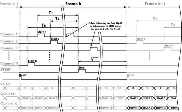
The chip is fabricated in 0.35 μm high-voltage CMOS tech-nology. While the chip reported in [23] includes only the TDC, with no detector, the new integrated circuit here described is composed by 16 independent smart pixels (SPAD plus TDC each), a common STOP channel and bias circuitry. Overall di-mensions are 5.9 mm × 1.5 mm, as shown Fig. 2, top. The chip allows 16 simultaneous and independent photon-timing measurements, with a conversion rate up to 2.5 Mconver-sions/channel. At the RESET rising edge, channels data are stored, then the falling edge enables the chip for a new acquisi-tion. When a SPAD detects a photon, a START signal triggers the corresponding TDC and the detector is disabled.
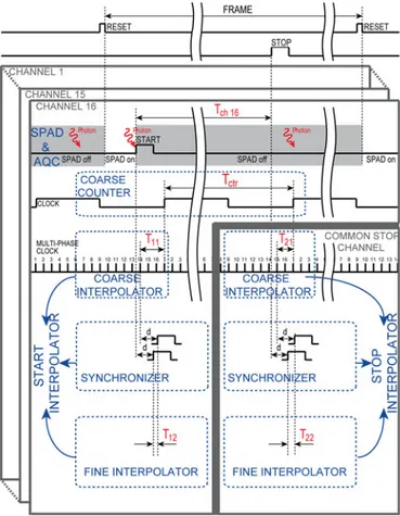
The TDC’s operating principle is depicted in Fig. 3: in each channel a counter counts the number (Ncounter) of clock rising
edges between START and STOP, then a two stage interpolator resolves the time (Tstart) between the START event and the next
Fig. 2. Microphotograph of the array chip (a) containing the 16 smart pixels, STOP channels and the global electronics for synchronizations and references. Architecture of the chip (b).
Fig. 3. Time measurement operating principle. In each pixel a counter counts 100 MHz clock cycles, between the photo-generated START and the STOP synchronism, then interpolators resolve both STARTs and STOP occurrence within each clock period, eventually reaching 10 ps resolution.
Fig. 4. Picture of the module, composed by three electronics boards: (top) monolithic chip with the 16 channels, reference clock, input signal conditioning stage for STOP signal; (center) FPGA board with USB 2.0 link; (bottom) switching power supply from the +5 V power plug.
STOP channel, resolves the time (Tstop) between the STOP
pulse and the next clock rising edge.
A common bus is used to read-out all data, via a 5 bit selector to address the sixteen 15 bit digital words of (START) photons and the single 15 bit word of STOP synch.
For each channel, the timing Tch data is given by the sum
of times measured by in-pixel counter and START interpolator minus the time measured by the STOP interpolator:
Tch= Ncounter· Tctr+ (T11+ T12)− (T21+ T22)
= Tcounter+ Tstart− Tstop
Since all interpolators are identical, the global electronics uses one DLL to provide every channel with 16 clock phases, which are needed by interpolators’ first coarse stage. Two ad-ditional DLLs are employed to create control voltages of fine interpolators’ VCDLs, guaranteeing 10 ps resolution.
The ASIC power consumption is less than 10 mW per pixel at low conversion rate and less than 15 mW at the maxi-mum conversion rate of 3 Mconversion/s, plus a contribution of 20 mW from the global electronics.
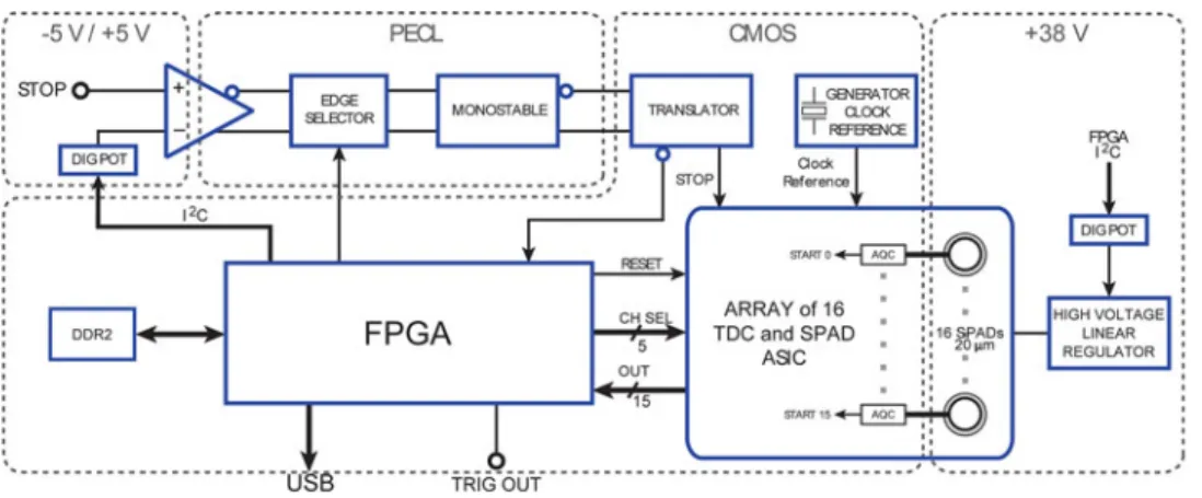
III. SYSTEMARCHITECTURE
The complete module is shown in Fig. 4 and is 6 cm× 6 cm × 10 cm. Fig. 5 shows a simplified block diagram of the module, whose main components are described in the followings. It is composed by three electronic boards around the core CMOS array chip, stacked one over the other. The top board hosts the CMOS chip, an extremely precise 100 MHz clock generator, and input signal conditioning electronics and an SMA connec-tor for external STOP signal. The middle board hosts a Xilinx XC6SLX45-2FGG484 Spartan-6 FPGA for processing, a 128 MiB DDR2 SDRAM for storing bulky TCSPC waveforms, and an USB 2.0 connector for PC interfacing. The bottom board manages all power supplies, from a 5 V plug.
Fig. 5. Block diagram of the module. A crystal oscillator provides the 100 MHz reference clock. The STOP synchronism is signal-conditioned before feeding the array chip. An FPGA manages the overall electronics and uploads TCSPC data via USB 2.0 interface.
A. Input Signal Conditioning Electronics
The array chip accepts 3.3 V CMOS levels, therefore a front-end signal conditioning circuit is needed in order to deal any possible user’s signal (CMOS, TTL, ECL, NIM, and even non-standard signals, either positive or negative edge-triggered). The STOP input of the module feeds a fast comparator (ADCMP561 by Analog Devices), powered at±5 V, whose threshold is set by an 8 bit digital potentiometer, controlled by the FPGA via I2C serial protocol, in the range from−2 V to +3 V, with a resolu-tion of 19.5 mV steps. The comparator PECL logic output pro-vides fast differential signals in order to minimize additive time jitter.
The differential output drives an edge selector stage, made by transistors and high-pass filters, that provides a short positive pulse to trigger the monostable stage at the edge selected by an FPGA control pin. The monostable circuit is based on a PECL OR gate with an high-pass filter in feedback loop, which provides a pulse of 10 ns fixed duration to the array chip, through a level translator that converts the OR gate PECL output to a +3.3 V standard CMOS level [24].
B. Control and Data Processing Electronics
The FPGA is in charge of three main tasks. The first one is to receive the settings selected by the user on the PC graphical user interface and to configure the module accordingly. For instance, the FPGA sets the STOP input threshold level by means of a digital potentiometer configured via I2C protocol, and also selects the input trigger edge. Other settings are the trigger out frequency and the SPADs reverse bias.
The second task of the FPGA is to control chip operations (by monitoring the STOP signal and by properly acting on the RESET pin after each maximum conversion time) and to acquire the raw content of Ncounter and Nstartout from each pixel and
Nstop data (by properly acting on the SEL selection bus and
by reading the chip output bus), as shown in Fig. 6. This task is implemented via a state machine, then the raw data must be processed in order to obtain the final measurement results. The conversion is performed in the FPGA using hardware adders and multipliers and the calibration LUT, giving as a final result the
photon time-interval measured by the channel. This processing is then repeated for all 16 channels.
The third FPGA task is to transfer the measurements to the PC. In order to be able to transfer all data acquired by the chip even at the maximum counting frequency, conversion results are temporarily stored into a 128 MiB DDR2 SDRAM, which is then periodically read to upload its contents to the remote PC via the USB 2.0 interface. The resulting maximum effective throughput is 40 Mconversion/s, i.e. a maximum photon rate of 2.5 Mphotons/s per pixel.
C. Power Supply
All necessary power supplies are derived from a +5 V DC unregulated supply. The required voltages are:±5 V for the first signal-conditioning stage; +3.3 V for the PECL and CMOS log-ics; and +35 V for the SPADs bias. These voltages are generated by DC/DC switching converters, placed on the separate power supply board, and LDO regulators, placed on the timing board, in order to guarantee separate voltages to different module blocks to preserve minimal mutual interference. A programmable dig-ital potentiometer sets the high voltage linear regulator’s in-put voltage, in order to have the possibility to change the re-verse bias SPAD voltage, i.e. the effective excess voltage above breakdown.
The overall power supply board efficiency is 80%, result-ing in 3.25 W total power consumption for the overall module operating at maximum conversion rate.
D. Software Interface
The software interface gives the user the possibility to quickly set configuration parameters, like SPAD excess bias and frame rate, STOP input threshold and trigger (rising or falling) edge. Measurements can be either free-running (i.e. data is acquired until the user stops the measurements) or fixed-duration (it stops after a fixed time, set by the user).
The software displays the histograms of the measured time-intervals for each selected channel, together with an addi-tional histogram representing the amount of conversions per each channel. The interface also displays a table with main
Fig. 6. Timings of main chip signals. Each channel provides its START when a photon is absorbed in that SPAD; the RESET rising edge makes the conversion results available for readout, while its falling edge resets the chip for a new conversion. Each 15 bit channel word is selected through a 5 bit “Ch sel” address. Since data is read-out during a new conversion, each channel can work up to 2.5 Mcps photon rate.
information about the ongoing measurement, such as the total number of conversions, the average conversion rate per channel, the trace’s peak positions, their FWHM, etc. The measurement data can be saved as textual file, which can be later retrieved for reviewing the results or for resuming a paused measurement.
IV. EXPERIMENTALRESULTS
We carried out in-depth characterizations of both detection and timing performances of the chip and the overall module.
A. SPAD Performances
The 20 μm active-area diameter SPADs designed in this 0.35 μm CMOS technology [25] have a breakdown voltage of 28 V. Concerning yield, Fig. 7 reports the measured dark-count rate (DCR) at 5 V excess bias and room temperature of 300 SPADs: about 75% of the detectors show a noise below 4 kcps and 92% are below 100 kcps.
Fig. 8 shows the spectral photon detection efficiency (PDE) at different excess bias. The peak PDE at 5 V excess voltage is 43% at 450 nm wavelength and still 10% at 750 nm.
Another important noise contribution is afterpulsing proba-bility [11], [22], i.e. the chance of an avalanche to be ignited by charge carriers released after been trapped during a previ-ous avalanche pulse. As Fig. 9 shows, afterpulsing can be kept below 6% by keeping the SPADs off for a dead-time of 200 ns after the ignition. This is not a limiting factor because the chip intrinsically keep the SPAD turned off at least 200 ns. This is due to maximum conversion dead of 150 ns time, plus signals
Fig. 7. Cumulative distribution for dark-counting rate of about 300 SPADs at 5 V excess bias, at room temperature (RT) and 5°C.
propagation delay of about 20 ns due to traces length and FPGA routing, plus RESET signal duration of 30 ns.
B. Module Performances
The sole TDC cannot be characterized because its START signal is not accessible outside the chip. Therefore we charac-terize the performances of the whole system by triggering the corresponding SPAD.
The relevant parameters are single-shot precision, measured as the FWHM of each channel, skew between channels, DNL and crosstalk (both optical and electrical).
Fig. 8. Typical spectral detection efficiency of the SPADs at different excess bias applied to the SPADs.
Fig. 9. Total afterpulsing probability at different excess bias and hold-off times, for the 20 μm diameter SPADs.
First of all, TDC linearity was evaluated through a code den-sity test. A periodic STOP signal was provided to the module, while keeping the detectors covered, thus obtaining a random (due to dark counts) uniformly distributed START pulse over the whole TDC full-scale range. This measure requires a very large number of samples (at least 10 k conversions per histogram bin). Considering an ideal SPAD, the reconstructed histogram reflects the non-linearity of the converter, after subtracting the mean amplitude. However, when the SPAD has a non-negligible afterpulsing, the histogram includes also the afterpulsing trend, which needs to be deconvolved for computing the module non-linearity. In conclusion, we measured a DNL of less than 5% LSB peak and 1.5% LSB rms.
In arrays of SPAD-based pixels, crosstalk is mainly optical in nature, as it is related to photons emitted by hot carriers in an avalanching pixel that get reabsorbed in a neighboring chan-nels [26]. This effect is proportional to the total charge flowing through the SPAD. Here we measured an overall crosstalk
prob-Fig. 10. Channels timing response at different excess bias and at 820 nm.
ability among adjacent channels of less than 1· 10−4, including both electrical and optical contributions.
Overall timing precision of the SPAD-triggered TDC was measured by focalizing a short laser pulse (with FWHM <10 ps) at 820 nm on the chip. After a large number of measurements, precision was computed as the FWHM of the measurement dis-tributions around the mean value. Multiple acquisitions were performed at different SPAD excess bias voltages, as shown in Fig. 10, thus obtaining an average value of 70 ps FWHM. Such mean value proved to be quite constant over the en-tire TDC full-scale range, as reported for the single TDC in [23].
The module is fairly insensitive to the conversion rate, as the mean value of the measurement distribution changes by less than 1 LSB (i.e. 10 ps) when the laser repetition frequency is changed by two decades, from 25 kHz to 2.5 MHz, while the FWHM remains nearly the same.
The maximum skew among all channels is shorter than 60 ps, as shown in Fig. 11, and it is caused by the different propaga-tion delay of the STOP signal from the input pin to the various channels. Since this effect is deterministic, it can be corrected in post-processing or on-board within the FPGA. The slow ex-ponential tail is typical of SPADs [11] and has a time constant of about 200 ps.
TABLE I
COMPARISON OFMODULEPERFORMANCEWITHSIMILARSOLUTIONSREPORTED INLITERATURE
Parameter [13] [14] [15] [16] This work
Technology[μm] 0.13 0.13 0.13 0.13 0.35
Array dimension[pixel] 32× 32 32× 32 160× 128 64× 64 16×1
TDC Measurement range[ns] 55 100 55 64 160 TDC Dead Time[ns] - - 100 - 150 TDC Resolution (LSB)[ps] 52 119 55 62.5 10 TDC Accuracy (FWHM)[ps] 70 185 - - 40 DNL[%LSB] 40 40 30 400 5 peak, 0.9 rms System Accuracy (FWHM)[ps] - 230 140 - 70 TDC Power Supply[V] 1.2 1.2 - 1.5 3.3
SPAD active area diameter[μm] - 8.6 5.6 5 20
SPAD DCR at Room Temperature[cps] - 100 at VE X = 1 V 50 at VE X >= 0.73 V 1036 at VE X = 2.5 V 4000 at VE X = 5 V
90000 at VE X = 2 V
SPAD Yield[%] - 60 70 - 75
SPAD Max. Photon Detection Efficiency[%] - 25 27.5 30 43
SPAD Power Supply[V] - - - 12 35
ASIC Maximim Frame Rate[MHz] 1 1 - - 2.5
ASIC Maximum Power Consumption[mW] 45 (core only) 90 (core only) 550 8790 275
Fig. 11. Timing response of all 16 channels, under a 10 ps laser pulse at 820 nm. The average FWHM of timing responses is about 70 ps, while the maximum peak skew among channels is less than 60 ps.
V. CONCLUSIONS
We presented a very compact TCSPC module, which pro-vides high performance time-resolved single-photon detec-tion (through 16 SPAD detectors) and photon-timing measure-ments (via 16 in-pixel TDCs) with 10 ps resolution, 70 ps (FWHM) precision, better than 1.5% LSB (rms) DNL, and up to 2.5 Mcps photon rate per channel (see Table I for a perfor-mance summary and a comparison with similar solutions re-ported in literature). The single photon sensitivity spans from the near-ultraviolet (30% at 300 nm) to the near-infrared (still 1% at 950 nm) range, with a 43% peak at 450 nm, with very low power consumption of 3.25 W, when operated at an average detection rate of 2.5 Mconversion/s per channel. The module’s core is a monolithic array chip designed in a cost-effective 0.35 μm CMOS technology, consisting of 16 channels composed by a TDC and a silicon SPAD each. The ASIC constitutes an in-termediate step towards the development of large 2-D arrays
(i.e. 16 × 16 or 32 × 32 smart pixels). In order to reach this goal some power efficiency optimizations are needed to keep the overall consumption low.
This module opens the way to a large number of demand-ing applications, requirdemand-ing multi-channel acquisitions of fast and faint optical waveforms at the single-photon and picosec-ond level, including applications like FLIM, FRET, FCS, and DOT where very compact dimensions and many independent channels working in parallel are a must.
REFERENCES
[1] W. Becker, Advanced Time-Correlated Single Photon Counting
Tech-niques. Berlin, Germany: Springer, 2005.
[2] D. Contini, A. Torricelli, A. Pifferi, L. Spinelli, F. Paglia, and R. Cubeddu, “Multi-channel time-resolved system for functional near infrared spec-troscopy,” Opt. Exp., vol. 14, pp. 5418–5432, 2006.
[3] W. Becker, A. Bergmann, M. A. Hink, K. Konig, K. Benndorf, and C. Biskup, “Fluorescence lifetime imaging by time-correlated single-photon counting,” Microsc. Res. Tech., vol. 63, pp. 58–66, 2004. [4] W. Becker, A. Bergmann, and C. Biskup, “Multispectral fluorescence
lifetime imaging by TCSPC,” Microsc. Res. Tech., vol. 70, pp. 403–409, 2007.
[5] C. Biskup, T. Zimmer, L. Kelbauskas, B. Hoffmann, N. Klocker, W. Becker, A. Bergmann, and K. Benndorf, “Multi-dimensional fluo-rescence lifetime and FRET measurements,” Microsc. Res. Tech., vol. 70, pp. 442–451, 2007.
[6] W. Becker, K. Benndorf, A. Bergmann, C. Biskup, K. Konig, U. Tirlapur, and T. Zimmer, “FRET measurements by TCSPC laser scan-ning microscopy,” Proc. SPIE, vol. 4431, pp. 94–98, 2001.
[7] P. Kapusta, M. Wahl, A. Benda, M. Hof, and J. Enderlein, “Fluorescence lifetime correlation spectroscopy,” J. Fluorescence, vol. 17, pp. 43–48, 2007.
[8] W. Becker, A. Bergmann, A. Gibson, N. Everdell, D. Jennions, M. Schweiger, S. R. Arridge, and J. C. Hebden, “Multi-dimensional time-correlated single photon counting applied to diffuse optical tomography,”
Proc. SPIE, vol. 5693, pp. 34–42, 2005.
[9] W. Becker, A. Bergmann, H. Wabnitz, D. Grosenick, and A. Liebert, “High-count-rate multichannel TCSPC for optical tomography,” Proc.
SPIE, vol. 4431, pp. 249–254, 2001.
[10] X. Michalet, O. H. W. Siegmund, J. V. Vallerga, P. Jelinsky, J. E. Millaud, and S. Weiss, “Detectors for single-molecule fluorescence imaging and spectroscopy” J. Modern Opt., vol. 54, pp. 239–281, 2007.
[11] F. Zappa, S. Tisa, A. Tosi, and S. Cova, “Principles and features of single-photon avalanche diode arrays,” Sens. Actuators A, Phys., vol. 140, pp. 103–112, 2007.
[12] A. Cuccato, S. Antonioli, M. Crotti, I. Labanca, A. Gulinatti, I. Rech, and M. Ghioni, “Complete and compact 32-channel system for time-correlated single-photon counting measurements,” IEEE Photon. J., vol. 5, no. 5, p. 6801514, 2013.
[13] J. Richardson, R. Walker, L. Grant, D. Stoppa, F. Borghetti, E. Charbon, M. Gersbach, and R. K. Henderson, “A 32× 32 50 ps resolution 10 bit time to digital converter array in 130 nm CMOS for time correlated imaging,” in Proc. IEEE Custom Integr. Circuits Conf., 2009, pp. 77–80. [14] M. Gersbach, Y. Maruyama, R. Trimananda, M.W. Fishburn, D. Stoppa,
J. A. Richardson, R. Walker, R. Henderson, and E. Charbon, “A time-resolved, low-noise single-photon image sensor fabricated in deep-submicron CMOS technology,” IEEE J. Solid-State Circuits, vol. 47, no. 6, pp. 1394–1407, Jun. 2012.
[15] C. Veerappan, J. Richardson, R. Walker, D. Li, M.W. Fishburn, Y. Maruyama, D. Stoppa, F. Borghetti, M. Gersbach, R. K. Henderson, and E. Charbon, “A 160× 128 single-photon image sensor with on-pixel 55 ps 10 b time-to-digital converter,” in Proc. IEEE Int. Solid-State Circuits
Conf. Dig. Tech. Papers, 2011, pp. 312–314.
[16] R. M. Field, S. Realov, and K. L. Shepard, “A 100 fps, time-correlated single-photon-counting-based fluorescence-lifetime imager in 130 nm CMOS,” IEEE J. Solid-State Circuits, vol. 49, no. 4, pp. 867–880, Apr. 2014.
[17] F. Villa, B. Markovic, S. Bellisai, D. Bronzi, A. Tosi, F. Zappa, S. Tisa, D. Durini, S. Weyers, U. Paschen, and W. Brockherde, “SPAD smart-pixel for time-of-flight and time-correlated single-photon counting measure-ments,” IEEE Photon. J., vol. 4, no. 3, pp. 795–804, Jun. 2012. [18] Y. Maruyama, J. Blacksberg, and E. Charbon, “A 1024× 8, 700 ps
time-gated SPAD line sensor for planetary surface exploration with laser raman spectroscopy and LIBS,” IEEE J. Solid-State Circuits, vol. 49, no. 1, pp. 179–189, Jan. 2014.
[19] C. Scarcella, A. Tosi, F. Villa, S. Tisa, and F. Zappa, “Low-noise low-jitter 32-pixels CMOS single-photon avalanche diodes array for single-photon counting from 300 nm to 900 nm,” Rev. Sci. Instrum., vol. 84, no. 12, pp. 123112-1–123112-5, 2013.
[20] Becker&Hickl GmbH. SPC-130 data-sheet (2010).[Online]. Available
http://www.becker-hickl.de/
[21] PicoQuant GmbH. PicoHarp300 data-sheet (2010).[Online]. Available
http://www.picoquant.com/
[22] S. Tisa, F. Zappa, A. Tosi, and S. Cova, “Electronics for single pho-ton avalanche diode arrays,” Sens. Actuators A, Phys., vol. 140, no. 1, pp. 113–122, 2007.
[23] B. Markovic, S. Tisa, F. A. Villa, A. Tosi, and F. Zappa, “A high-linearity, 17 ps precision time-to-digital converter based on a single-stage vernier delay loop fine interpolator,” IEEE Trans. Circuits Syst. I, Reg. Papers, vol. 60, no. 3, pp. 557–569, Mar. 2013.
[24] B. Markovic, D. Tamborini, F. Villa, S. Tisa, A. Tosi, and F. Zappa, “10 ps resolution, 160 ns full scale range and less than 1.5% differential non-linearity time-to-digital converter module for high performance timing measurements,” Rev. Sci. Instrum., vol. 83, no. 7, pp. 074703-1–074703-10, 2012.
[25] S. Tisa, F. Guerrieri, and F. Zappa, “Variable-Load Quenching Circuit for single-photon avalanche diodes,” Opt. Exp., vol. 16, pp. 2232–2244, 2008. [26] I. Rech, A. Ingargiola, R. Spinelli, I. Labanca, S. Marangoni, M. Ghioni, and S. Cova, “A new approach to optical crosstalk modeling in single-photon avalanche diodes,” IEEE Photon. Technol. Lett., vol. 20, no. 5, pp. 330–332, Mar. 2008.