Università degli Studi di Catania
D ottorato di Ricerca in Fisica – XXIII ciclo
_______________________________________________________________LOREN ZO N ERI
Time Resolved Single Photon Imaging Sensor
w ith Single Photon Avalanche D iode
PhD Thesis
PhD Coordinator: Tutor:
Prof. Francesco Riggi Prof. Francesco Mu su m eci
IN FN -LN S Tutor:
II
Per diletto cerco i perché della Fisica,
Per fortuna ho trovato i perché della mia vita,
Valeria ed Alessio.
III
Contents
INTRODUCTION ... 1
1. SPAD DEVICE ... 4
1.1 JUNCTION DESIGN AND AVALANCHE PROCESS ... 4
1.2 VOLTAGE SUPPLY AND I-VCHARACTERISTIC ... 7
1.3 QUENCHING SYSTEMS ... 8
1.4 AFTERPULSE ... 10
1.5 RECHARGE AND DEAD TIME ... 14
1.6 DARK NOISE ... 15
1.7 SECONDARY PHOTONS ... 17
1.8 CROSS TALK ... 18
1.9 PHOTON DETECTION EFFICIENCY ... 21
2. SPAD ELECTRIC SIMULATION... 23
2.1 ELECTRIC SPADMODEL ... 23
2.2 CALIBRATION MEASUREMENTS ... 27
2.3 PQC WITH GROUND ON CATHODE ... 31
2.4 COMPARISON BETWEEN MEASURED AND SIMULATED SIGNAL ... 33
2.5 SPADDOUBLE READOUT CONFIGURATION ... 34
2.6 ARRAY CONFIGURATION ... 38
2.7 PROTOTYPE:BINARY INDEXING READOUT ... 40
3. SPAD COUNTING CORRECTION ... 45
3.1 SIMULATION TECHNIQUE ... 45
IV
3.1.2 Dead Time Simulation ... 49
3.1.3 Noise Simulation ... 51
3.2 COUNTING CORRECTION ... 53
3.2.1 Dead Time Correction In Geiger-Muller Device ... 54
3.3 SPADDEAD TIME CONFIGURATION ... 55
3.4 SPADNOISE CORRECTION ... 57
3.4.1 Simulation Validation ... 58
3.4.2 Experimental Validation ... 59
3.5 AFTERPULSE ... 60
3.6 SPADDEAD TIME CORRECTION ... 61
3.7 VARIANCE-TO-MEAN RATIO ... 64
3.8 COMPARISON BETWEEN PASSIVE AND ACTIVE QUENCHING ... 65
3.9 APD:CONFIGURATION WITHOUT DEAD TIME ... 66
3.10 RESULTS ... 69
4. GENERALIZATION OF DT EQUATIONS FOR TIME DEPENDENT SOURCES ... 71
4.1 LITERATURE TIME DEPENDENT APPROACHES ... 72
4.2 NEW DEAD TIME EQUATIONS ... 72
4.2.1 Non Paralyzable Dead Time ... 72
4.2.2 Paralyzable Dead Time ... 74
4.2.3 Hybrid Dead Time ... 75
4.2.4 Relation Between Non Steady-State and Steady-State Equations ... 76
4.3 MONTECARLO SIMULATIONS ... 77
4.4 EXPERIMENTAL VALIDATION ... 79
4.4.1 Materials ... 79
4.4.2 Validation ... 80
4.5 RESULTS ... 83
5. SPAD IMAGING DEVICE ... 84
5.1 STATE OF ARTS OF TIME RESOLVED AND HIGH SENSIBILITY APPROACHES . 85 5.2 INNOVATION IN MATRIX DESIGN ... 88
5.3 SPADIMAGING DEVICE FABRICATION ... 90
5.4 FRONT-END ELECTRONICS ... 93
V
5.6 COINCIDENCE... 101
5.7 TIMING PERFORMANCE AND MATRIX DESIGN ... 108
5.8 RESULTS ... 110
CONCLUSIONS AND PERSPECTIVES ... 112
BIBLIOGRAPHY ... 115
Introduction
The main topic of this work is the study of a new optical sensor with perfor-mances that will extend capability of new physical investigation techniques. Ex-treme detection efficiency was bring to the single photon sensibility, arriving time measurement was achieved with subnanosecond precision and the spatial recognition was obtained with two-dimensional integrated device. Maximum frame rate achievable is the single photon detection and no break is needed for device readout process.
These characteristics make the sensor, that we have studied, very attractive in several techniques which represent the state of the art of analysis methods, in solid Physics, Biology, and Astronomy. Fluorescence Lifetime Imaging Micro-scopy (FLIM)[1] is a functional imaging methodology that can provide informa-tion, not only concerning the localization of specific fluorophores, but also about the local fluorophores environment. It may be implemented in scanning confocal or multi-photon microscopes, or in wide-field microscopes and endoscopes. When applied to tissue autofluorescence, it reveals intrinsic excellent contrast between different types and states of the tissue. Nanosecond time domain, imag-ing, and extremely low light emission rate of environments investigated with this technique are exactly the scope of our sensor. Actually this technique is made with a single pixel sensor and to obtain an imaging a scanning procedure was used, with our sensor the imaging is a native characteristics that enable faster and more compact new setups. Many other investigation techniques, need same features, and for each of them our sensor is able to allow a step forward. Time Correlated Single Photon Counting (TCSPC)[2] is the base of FLIM but also many others exciting analysis technique like Dynamic Light Scattering analysis (DLS)[3], by which, for example, it is possible to determine dimension and
2
shape of particle in suspension and the interaction with the solvent[4]. Time pre-cision reached with our device make also possible the implementation of 3D camera[5] in which the third dimension comes from the registration of the light reflection delay. High frame rate achievable with our imaging sensor enable fast transient analysis like Particle Imaging Velocimetry (PIV)[6] and Adaptive Op-tics (AO) [7], used in optical ground-based astronomy and space surveillance, to enable real time aberrations corrections, introduced by the atmospheric turbu-lence.
Our time resolved single photon imaging sensor is based on silicon semicon-ductor technology. Beyond the detection performance it takes advantages from many features that are intrinsic of the technology. First of all, is insensitive to magnetic field, requires a low voltage source and a low power source, benefits from miniaturization technology, is robust and shockproof, benefits from low cost fabrication process, and last but not least is at the same time sensible to the single photon and not damageable by any extremely high light intensity.
The research work performed and reported in this thesis has been absorbing and exciting, because all the aspects of the sensor developing have been studied.
In chapter 1 we have studied the physical characteristics, the sensing fea-tures and the noise suffering of the elementary sensing device of our sensor, the Single Photon Avalanche Diode (SPAD)[8]. We have continued, in chapter 2, the study of the single device by developing an electric characterization proce-dure and a electric simulation, studying different signal extraction techniques and testing two-dimensional electric configuration. Pushed by the objective to extend the counting range of the passive quenched SPAD, we have developed, in chapter 3, a simulation code and dedicated experimental measurement setups, to study the dynamic properties of sensor. Dead Time, detection efficiency, noise, and afterpulse, was studied to predict and correct their counting distortion. In the chapter 4 we explain one of the most relevant result obtained in this work, we was able to extend the dead time correction know in Literature over the steady state analysis to the time dependent source. The relevance of the obtained re-sults, already published on “Sensors” journal[9], has been that they can be ap-plied to all the device that are subjected to dead time and not only to the SPAD
1.1 Junction Design and Avalanche Process
3
devices. In the last chapter we have dealt with the high performance imaging topic, we have shown our personal solution in the two-dimensional SPAD confi-guration, we have described the imaging extraction procedure, and finally ex-amined the peculiarity and the limits of our approach.
1. SPAD Device
The Single Photon Avalanche Diode (SPAD)[10] is the new generation of Geiger-Muller (G-M) detectors developed in semiconductor technology for pho-ton counting measurement. This device enables the highest possible light sensi-tivity, that means the single photon sensisensi-tivity, the precise measure of the light time distribution also for very fast pulse and the possibility to achieve the corre-lation analysis of photons arrival time. In the last years many applications look to these features and SPAD development reach high level performance. Many products were already commercialized, and many applications were considered affordable for future SPAD technology. The imaging sensor studied in this PhD work is based on SPAD and in particular we used devices fabricated in Catania by the local STMicroelectronics R&D center. The aim of this chapter is an over-view of SPAD device working principles, performance and technical characte-ristics, especially taking in account aspects concerning imaging sensor design. A deeper analysis of SPAD electric characteristics and features related to the imag-ing detector will be presented in the next chapter 2.
1.1 Junction Design and Avalanche
Process
When a photon is absorbed inside a semiconductor an electron-hole pair is generated. If the photon is adsorbed inside a depletion region in which an elec-tric field is present an elecelec-tric field the electron and the hole drift according to their electric charge. This is the working principle of the photo-diodes, in which a big amount of photons are translated in an electric signal. To detect less
pho-1.1 Junction Design and Avalanche Process
5
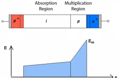
tons, and at the extreme a single photon, a multiplication process should be acti-vated. This is simply achievable in the semiconductor device increasing the ap-plied electric field. If enough energy is provided to the free charges, the impact ionization can be enabled, and the electrons and the holes can extract other charges from the atoms of the material, multiplying their total number until a macroscopic electric signal is obtained. The impact ionization probability is strongly dependent from the electric filed inside the semiconductor, so can be finely and easily regulated with the voltage modulation. With such prescription high detection efficiency devices can be realized, the Avalanche Photon Diode (APD) and the Single Photon Avalanche Diode (SPAD). A specified junction design of the first type is the Separated Adsorption and Multiplication APD (SAM APD) shaped with a large depletion region followed by a multiplication region (Figure 1-1). This design is focused to reach high efficiency, due to the large adsorption region, and to a fine selection of the multiplication factor in the p doped region, in which there is generated the high electric field. Electric field trend is pointed out in the Figure 1-1. With this device it is possible to detect quite low photon flux because of the limited multiplication factor. The single photon detection is difficult, because of the large statistical fluctuation on the multiplication process.
Figure 1-1: Junction scheme of SAM APD device and electric field generated inside the junction.
6
Typical multiplication factor ranges from hundreds to thousands of charges for each adsorbed photon. The produced signal follows the shape of the imping-ing photon flux.
The SPAD device is designed with an high doped p+ n+ junction, operating with a voltage 10% or 20% greater than the impact ionization potential. The junction SPAD design requires a special attention to prevent the early break-down that could occur at the edge of the junction. In this region the peak effect generates an inhomogeneous electric field with peak values that make easier the generation of high noise rate production. The solution is to surround the deple-tion region with a n doped region to confine homogeneously the electric field (Figure 1-2).
Figure 1-2: Junction scheme of SPAD device.
In SPAD device the adsorption area and the multiplication region are the same, in correspondence of the depletion region n+ p+. The sensitivity reach the single photon detection threshold with the overvoltage. The rapidity of impact ionization process produce a rapid growth of an electric signal that can be used as time information of the single photon adsorption event. Typically subnanose-cond accuracy has been reached.
1.2 Voltage Supply and I-V Characteristic
7
1.2 Voltage Supply and I-V
Characte-ristic
The junction design used for the SPAD device (Figure 1-2) can be also used in APD mode by modulating the power source. The impact ionization multipli-cation factor, modulated by the applied voltage, varies with the shape, as shown in Figure 1-3. The impinging photon flux generates holes and electrons that, multiplied inside the junction, generate the current value showed in Figure 1-3. In the first part of the inverse polarization region, used for the photodiodes, the multiplication factor is zero and big amount of photon must be collected to pro-duce an electric signal. Starting from a value called VAPD the single pair
pro-duced by photon is multiplied along its trip, the generated charge amount is col-lected by anode and cathode metal contacts. After the breakdown voltage VB
value the impact ionization probability guarantee that each charge that flows through the junction generates others charge. Each charge before the end of its trip produces a charge of opposite sign that must cross the whole junction in the opposite direction, and so it is subjected to another impact ionization, producing an endless process. This is the self-sustaining avalanche process that is active until the applied voltage is over the breakdown value VB.
8
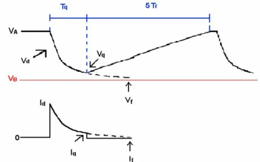
The SPAD device purpose is the single photon counting. By operating over the breakdown voltage the detection of a photon generates a self sustaining ava-lanche. In order to avoid the thermal junction destruction and to enable the fol-lowing events detection it is necessary to lower the applied voltage after the gen-eration of the signal, with the scope of quenching the avalanche, and, after that, recover the voltage to the initial state. This cycle is represented in the Figure 1-4 where A is the overvoltage condition without the avalanche, B is the current flowing point in the avalanche state, and C is the quenching of the avalanche state. This operating condition is called Geiger mode[11] because is the same of the Geiger-Muller counter device.
Figure 1-4: I-V characteristic of SPAD device operating in a Geiger mode.
1.3 Quenching Systems
There are two strategy for the quenching of SPAD, the use of a Passive Quenching Circuit (PQC)[12] or an Active Quenching Circuit (AQC)[13]. The PQC uses only one big resistor, while for AQC there are many possible ap-proaches and also hybrid configuration with passive quenching and active reset.
1.3 Quenching Systems
9
In this presentation of quenching features we point the attention on PQC because in our imaging application we have bet on the advantages of using only one re-sistor quenching circuit. The feature used by the PQC (Figure 1-6A) is the vol-tage drop on a resistor crossed by a current. When the avalanche current flow across a big resistor, typically few hundred of kΩ (RL in Figure 1-6A), the
vol-tage applied to the diode decreases (volvol-tage dropt, Vd in Figure 1-5).
According-ly the multiplication factor decreases and the outgoing current also decreases ex-ponentially. If the voltage decreasing the multiplication factor becomes less than the self-sustaining value, the impact ionization becomes a non sure event and the avalanche quenching becomes probable.
Figure 1-5: Voltage oscillation and current production during photon detection of SPAD device with PQC.
After the quenching of the avalanche the diode is brought back to a non con-ductive state. Starting from this point the diode and the stray capacitance (CS in
Figure 1-6B) were recharged with a charge that flows across the quenching re-sistor and the voltage is slowly restored to the initial value. The circuital scheme of the SPAD device was described by Cova[12] and reported in Figure 1-6B. Detailed electric analysis of the SPAD device will be discussed in chapter 3.
10
Figure 1-6: A) Passive Quenching Circuit. B) PQC SPAD equivalent circuit.
The basic idea of the AQC was simply to sense the rise of the avalanche pulse and reach back on the SPAD, forcing, with a controlled bias-voltage source, the quenching and the reset transitions in a short time. The fast transition was achieved to reduced losses in photon counting. Typical time reached by AQC was about 40 ns. However, the faster is the performance pursued, the high-er is the impact of afthigh-erpulse effect[15], which will be discussed in the next sec-tion, which has typical time constant of hundred of nanosecond.
1.4 Afterpulse
The defects in the semiconductor material or the damages caused by fabrica-tion process (ion implantafabrica-tion, diffusion, etc.) insert energetic levels inside the band structure of the semiconductor. Due to their low population, below the sa-turation, the levels located in the center of the gap act as trapping centers[16], that during the avalanche process collect electrons. Unfortunately the lifetime of these energetic levels cannot be regulated, typical values are from some tens to hundreds of nanosecond. If an electron is released when the SPAD biases
vol-1.4 Afterpulse
11
tage is over the breakdown value an avalanche is triggered and a noise event is generated. The biggest disadvantage of such type of noise is the time correlation with real events. In a device made to enable correlation analysis all the sources of correlated noise should be reduced as possible.
In AQC devices the rapid replacement of the initial voltage state enables the detection of most part of the released electrons. So in AQC devices the amount of trapped electrons must be minimized, and this is done with the reduction of the avalanche charge that flows during the detection pulse. Afterpulses that cha-racterize fast AQC device are typical more than 10%. It is also unavoidable that on increasing the AQC rapidity the detected afterpulse rate exponentially in-creases[14].
In devices with PQC the time needed to recover the initial voltage is of the order of microseconds or less and the afterpulse probability is very low. Even if a big amount of charges is produced during the avalanche, and some of them are trapped, the largest number is released during a non sensitive time, without pro-ducing any effects on the SPAD count.
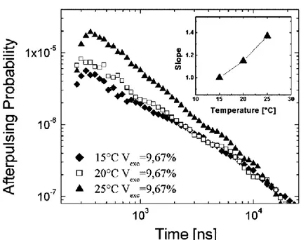
In our device we have used PQC configuration with low afterpulse produc-tion, but due to the relevance of correlated noise into a correlation detector we developed a detailed afterpulse analysis described in section 3.5. Our SPAD cha-racterization is focused on the realization of a imaging device, so the photon rate dependence has been deeply studied. We found that afterpulse counts decrease on increasing the photon rate. In the experimental data shown in Figure 1-7 the maximum afterpulse probability is around 3,5% before 8 Kcps and afterwards decreases until reach zero in correspondence to 50 Kcps. This reduction is gen-erated by the increase of the number of true events that trigger the diode before the afterpulse events generation.
12
Figure 1-7: Afterpulse probability vs impinging photon count rate.
A further parameter that influences the measured afterpulse count, for SPAD device in PQC configuration, is the threshold level. For this system the after-pulse is generated during all the recharge state, even if the only after-pulses that ex-ceed the threshold value are counted by the acquisition system. The histogram in Figure 1-8 shows the second pulse correlation in dark condition, measured by a digital oscilloscope. The histogram reports the delay between the first event and the following events that overcome the threshold level, like in real acquisition system. With a trigger level of -1,9 mV the histogram starts from 600 ns, while can be easily seen that the generation of new signals starts before. So, on chang-ing the trigger level, the amount of collected second signals changes. Due to the dark condition, the total amount of collected delays are caused not only by after-pulse, but they are mixed with the dark noise production. In fact dark noise pro-duction follows the Poissonian distribution, and the delay between events shows an exponential distribution with a time constant more close to the afterpulse dis-tribution. Inside the “Measure” box of the digital oscilloscope Figure 1-8 the mean of the P2:edge measurement shows a value of 1.09 , from this value 9% of second pulse inside the nine following microseconds can be deduced, and this is not only the afterpulse contribute, but the sum of afterpulse and the second ran-dom Poissonian dark noise.
1.4 Afterpulse
13 Figure 1-8: Digital Oscilloscope image in persistent mode with afterpulse measurement mode.
In conclusion, on increasing the threshold level, that means an increase of sensor dead time (DT), we obtain a desirable reduction in afterpulse measure-ment, but also a loss of true events. So the selection of the good threshold level should be taken into account the recharge process and the afterpulse production.
Another important parameter that modifies the afterpulse production is the temperature of the diode. Usually, to reduce the thermal noise of silicon device the temperature is lowered: usually a temperature of -20°C is considered in high sensitivity CCD camera. In Figure 1-9 the time distribution of the afterpulse probability is shown for three different temperature, 25°C, 20°C and 15°C. The insert of Figure 1-9 shows that the slope of the afterpulse probability linearly de-creases on decreasing the temperature. Taking into account that the temperature variation is of only 10°C, the slope trend clearly shows that at -20°C the SPAD cannot be used because with such lower temperature the largest amount of after-pulse overcome the dead time of the device. Due to this consideration the selec-tion of the SPAD working temperature must be chosen taking in account after-pulse and noise thermal characteristics.
14
Figure 1-9: Afterpulse time distribution for three different diode temperatures.
1.5 Recharge and Dead Time
In all counting device after the detection of an event it follows a time in which the device is not able to generate another count, this is called Dead Time (DT). There are two elementary idealized models of DT, named paralyzable (P-DT) and non paralyzable (NP-(P-DT). In the P-DT case all events occurring during the DT are not registered, but are able to prolong the period during which the de-tector is not able to reveal further signals. In the NP-DT case, any event arriving during the DT is neither registered nor has any influence on the device. In the real equipments parallel or series combinations of these two kinds of DT can be found.
For SPAD with AQC the DT is a fixed interval in which the impinging pho-tons are not collected nor produce any effects. The duration of this interval is well defined with the circuital design of the AQC system. In PQC SPAD the DT is a combination of the two DT types, and the incoming events can generate ef-fects even if they don’t generate counts.
1.6 Dark Noise
15
The avalanche process is a statistic process, the height of produced signal is strongly dependent from the overvoltage value, but it is also subjected to an in-trinsic random fluctuation of the avalanche generation process. During the re-charge of the diode the overvoltage grows according to a classical exponential trend of a resistor-capacitor recharge process. The amplitude of produced signal, that is linearly dependent from the overvoltage, follows this trend. According to the known shape of the recharge process, a fixed delay value necessary to obtain a signal that overcomes the threshold can be calculated. However the avalanche statistic fluctuation generates events that are detected earlier than predicted and loses events with time distant more than necessary. The fluctuation is not great compared with the total DT duration, but must be considered in the discussion. This is the reason of the first non zero value of the delay histogram in Figure 1-8. Another but more important effect of PQC SPAD is the production of non detected signals during the DT. In the Figure 1-8 it is clearly shown the high production rate of signals of amplitude lower than the threshold of the electron-ics. This signals do not produce counts but produces the restarting of the DT pe-riod, that means changes in the detection efficiency of the device. As described above the afterpulse losses inside the DT partially solve the problem of after-pulse phenomena, while the lost true events will be taken into account in the de-tailed DT analysis of chapter 3.
1.6 Dark Noise
In a SPAD device the primary noise source is the thermal assisted transition of an electron from the valence to the conduction band, that can be also seen like an hole production in the valence band. Both electron and hole can trigger an avalanche and so a signal can be produced, and unfortunately this signal cannot be distinguished from those produced by a photon. This noise is commonly called dark noise.
The electron and hole excitation mainly depends on the energy gap and on the temperature by the Arrhenius exponential factor e EKT . So the working temperature dominates the transition rate, and precise working temperature
con-16
trol must be implemented in SPAD sensors. Lowering the temperature reduces the thermal noise, but like showed previously (section 1.4) the temperature can be reduced until the afterpulse production remains below an acceptable level. The transition is also dominated by the concentration of crystallographic defect, that inserts shallow levels inside the gap. Such levels enable a two step transition (Figure 1-10) that is more probable of direct transition. So crystallographic de-fect become the most important source of noise, and fabrication technique should be addressed to reduce defect implantation.
Figure 1-10: Transition mechanisms of dark noise production.
It is important to note that the generation of a free pair inside the junction is a fundamental requirement for the noise production, as much as, the voltage ap-plied to the diode. Without enough voltage a free pair cannot be transformed into an avalanche and no noise signal is produced. So in the first part of the recharge process the lower voltage state inhibits the noise production. The overvoltage represents an avalanche efficiency that convert a single free pair into an ava-lanche. If the free pair comes from a thermal excitation we have a noise event, while if the pair comes from a photon adsorption we have a detection event. So the photon detection efficiency and the noise rate production are two strongly connected phenomena.
1.7 Secondary Photons
17
As it will be described in section 5.1 there are two main approaches to de-sign imaging device with SPAD technology, the first is the use of the smallest number of fabrication process optimized for SPAD device performances, the second is the use of CMOS technology that offers the possibility to merge SPAD design and complex electronics circuit facilities. Many performances can be in-creased with a dedicated technology development, first of all the dark count pro-duction that, as showed, is extremely dependent from the number and the type of the processes used in the fabrication. Our time resolved single photon imaging device approach is based on simplified SPAD fabrication. To use the higher per-formance enabled by this approach, all the needed acquisition electronic is de-signed outside the sensitive device.
1.7 Secondary Photons
During the avalanche process each ionization impact causes high decelera-tion in electron drift, so the Bremsstrahlung process enables a secondary photons production inside the junction. Due to the high photon sensitivity of SPAD de-vice the diffusion of these secondary photons must be controlled, and especially in array configuration. This photons production is contextual to the avalanche process so inside the diode don’t introduce delayed pulse as in the case of trap-ping phenomena. However the travelling photons outside the junction can exter-nally reflected and can generate delayed afterpulses if they are reflected back to the diode. In the device fabrication an antireflection coating layer is often added to prevent the photons emission outside the semiconductor device (Figure 1-2). Inside the STMicroelectronics fabrication process two antireflective layer were implemented, one made with silicon oxide and the other with silicon nitride. Be-fore of the deposition of these thin films the photons production is used, as fabri-cation check, to identify the avalanche spread along the diode surface. Figure 1-11 shows the images obtained by an Emission Microscope (EM), when differ-ent reverse currdiffer-ents flow through an avalanching junction. The images concern one of the diodes of the 10×10 SPAD array that will be discussed later in the chapter 5. The array was kept in dark condition, while the junction of the pixel
18
(1,1) was forced above breakdown at different excess biases, biasing the first anode row and cathode column. As it can be seen from the Figure 1-11, the breakdown is spatially uniform over all the active area, so excluding the possi-bility to have an edge breakdown fabrication defect. The different photons pro-duction for the two overvoltage values represent the different amount of ava-lanche charge produced.
Figure 1-11: Emission microscope pictures showing the avalanche turn-on in a pixel of 10×10 SPAD array at increasing overvoltage. Red means high, green lower, and blue lowest emission region.
1.8 Cross Talk
The downside of the high detection sensitivity of SPAD device is the cross talk between diode in array configuration. Actually the SPAD devices have a photon detection sensitivity of about 30% in the visible range, and 100% effi-ciency for free electron that travels in the biased junction. Two types of cross talk can occur between SPADs in array configuration, the optical and electric cross talk. For imaging application (chapter 5) or in Silicon Photon Multipliers application (SiPM)[17]-[18], many diodes have been putted the nearest possible to maximize the fill factor and the detection efficiency. On the other hand cross talk probability grows with SPAD density. Cross talk as afterpulse is a correlated noise, afterpulse is a time correlated while cross talk is a spatial correlated noise. In the imaging application the cross talk noise reduces the resolution with an out-of focus effect. Also in SiPM configuration, that do not require any spatial
1.8 Cross Talk
19
resolution, cross talk correlation activates neighboring pixels causing the degra-dation in the numerical determination of fired SPADs, so reducing the whole energy resolution of the device.
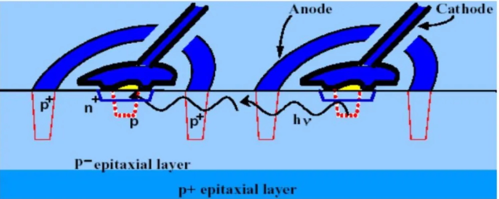
The optical cross talk is activated by the emission of secondary photons, that can travel along the silicon bulk, transparent to the optical wavelength, and cross another diode that is triggering a correlated avalanche (Figure 1-12). The time delay between the two produced signals is less than the measurable one and in-duced signals cannot be distinguished from the generated one.
Figure 1-12: Optical cross talk between SPAD diode in array configuration.
A further contribute to the optical cross talk was found[19] in the indirect optical pat (Figure 1-13) enabled by the optical reflection by the back part of the device.
20
The electric cross talk is activated by the electron current that travels, during the avalanche, along all the anode metallization of the device. In a matrix con-figuration the anode is shared between many diodes and the current flows near each diode junctions (see Figure 1-14).
Figure 1-14: Electrical cross talk.
The possibility that an electron can be collected by the biased cathode of an-other diode is very small, but, due to the high number of electrons, and the high detection efficiency of the other diodes, the electrical cross talk possibility can be significant. In addition the efforts in order to increase the fill factor, reducing the space between diodes, bring to a relevant optical and electric cross talk.
In order to study the reduction of the optical and electrical cross-talk contri-bution, arrays that are optically and electrically isolated by deep thin trench technology have been already designed and fabricated in Catania R&D group of STMicroelectronics. The developed trench process starts with a vertical etch 10 m deep and 1 m large and a subsequent oxide deposition for complete elec-trical isolation. Then the process continues with tungsten filling, to avoid optical cross-talk, and ends with planarization. The optical trench is showed in the left and right boundary of the Figure 1-15.
1.9 Photon Detection Efficiency
21 Figure 1-15: Schematic cross-section STMicroelectronics SPAD single pixel.
1.9 Photon Detection Efficiency
Silicon band gap is 1,12 eV. This energy corresponds to a photon with a wa-velength of 1100 nm. This is one of the boundary in the wawa-velength domain of the photons that can be detected by silicon device, SPAD included. The photon detection efficiency is modulated in wavelength by the absorption coefficient of light in silicon, and also by depends the junction dimension, the overvoltage val-ue and the diode temperature. The photon detection efficiency (PDE) of a SPAD device is given by the probability that a photon crosses the first part of the semi-conductor device without being adsorbed, multiplied by the adsorption proba-bility inside the active region. The adsorption probaproba-bility in a layer of thickness
dx at depth x is: dx x dx x P( ) exp( ) 1-1
where α is the absorption coefficient. In silicon this parameter varies with the photon wavelength as shown in Figure 1-16.
22
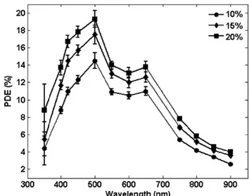
The resultant PDE (Figure 1-17) takes in account that, for high energy pho-tons, the adsorption coefficient is so big that a photon is adsorbed before the junction active region, while, for low energy photons, the probability to travel without adsorption in depth of the active region grows. The other parameters that affects the PDE of the device are not sensitive to the photon wavelength, but give only a quantitative contribute. As a result of the foregoing the thickness of the active region (the depletion region) is an important efficiency parameter. In-creasing the applied voltage increases the probability to start the avalanche process and so the detection probability. Figure 1-17 shows the PDE of a SPAD device measured[17] for different photon wavelengths and for different overvol-tage values. On increasing the overvolovervol-tage more than 20% the PDE do not in-crease linearly but reach a saturation level in which the avalanche process be-comes certain and a further increase do not produce any detection improve-ments. The PDE also shows a little dependence correlated to the working tem-perature of the device because of the little temtem-perature dependence of the semi-conductor bang gap, that was reduced increasing with the increase of the tem-perature.
Figure 1-17: Photon Detection Efficiency of SPAD device, for different wave length and different overvoltage values.
2. SPAD Electric
Simulation
The study of SPAD electric characteristics is fundamental to design two-dimensional array and its readout systems. In our work we develop a new rea-dout approach that minimize the number of rearea-dout channels. We need to under-stand the influence of diode electric characteristics on the shaping of the output signal, the realization of two readout signals for each SPAD, and the cross influ-ence between the diodes in the two-dimensional array configuration.
2.1 Electric SPAD Model
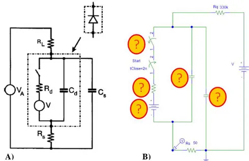
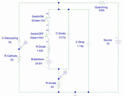
The SPAD electric model was deeply studied by Franco Cova[12], to devel-op fast active quenching circuit technology. We start from what published by Cova, shown in Figure 2-1A, to design a code for the SPAD electric simulation (Figure 2-1B). The PSpice[20] software suite was used. The simplest SPAD working configuration, the Passive Quenching Circuit (PQC), was used for the electric characteristics of diode electric components. With such basic configura-tion we are able to compare simulaconfigura-tion and measurement and extract the influ-ence of each electric components of the diode, that represent the electric aspects of the diode.
The charge separation inside the junction during the inverse polarization was simulated with the charge accumulated inside the capacitor Cd, where “d” means
24
avalanche process, and the breakdown voltage source V, with same polarity di-rection of the external power source, represents the voltage loss that do not take effect on the conduction mechanism. The avalanche process is equivalent to the “on” state of a switch, triggered by the photon adsorption, while the “off” state is before the adsorption and after the quenching of the avalanche. Single switch configuration used by Cova needs a complex code programming of a new PSpice switch components. To simplify the programming we selected, inside the PSpice library packs, two switches shown in Figure 2-1B, one that closes and the other opens the circuit. Both switches can be programmed with the time when their transition must occur. The others electric elements required for this confi-guration are the stray capacitance Cs, the quenching resistor RL, the applied
vol-tage VA, and the sensing resistor Rs.
Figure 2-1: Electric SPAD model: A) proposed by Cova; B) used for our simulation in-side PSpice programming suite.
While the value of the external quenching resistor, the applied voltage and the equivalent resistance of the readout electronic are well known, others values of the diode’s components and the stray capacitance must be evaluated. In Fig-ure 2-1B there are many question marks as the number of unknown value
2.1 Electric SPAD Model
25
meters. The transition time of the first switch, that closes the circuit, is not an important parameter because this time represents the photon adsorption, namely the zero time reference, and can be freely chosen. Differently the time transition parameter of the second switch, that represents the end of the avalanche quench-ing process, must be estimated. This parameter is connected to the end of the output signal and to the start of the recharge process.
Using the electric simulation program we can reproduce the output signal of the system, but, more importantly, we can understand how the SPAD circuit works, which are the reciprocal influences of its components, and then how the readout system can be designed to achieve our requirements.
When avalanche process closes the first switch three loops are closed, each one is shown in the Figure 2-2 with a different image. The three closed circuit share the left branch of the diode, composed by the two switches, the diode re-sistor and the breakdown voltage supply. The more external loop, Figure 2-2A, is composed by the common branch, the quenching resistor, the external voltage source, and the sensing resistor. Due to the high resistivity of this closed circuit the current that flows in correspondence of the avalanche start is some micro Ampere, and the signal that is produced in the sensing resistor is negligible. Also the diode internal loop (Figure 2-2C), that do not include the sensing resistor, is not the cause of the output signal. The source of the output signal is the loop that includes the stray capacitance (Figure 2-2B). When the avalanche closes the circuit the capacitance is discharged and a signal is produced across the sensing resistor. In this occasion the stray capacitance is not an unwanted effect but a fundamental element for the signal production. An important thing to underline is that the sensing loop (B) have the same characteristics of the diode internal loop (C). The total resistivity of the two loops are practically the same, because the internal resistor is some thousand of ohm as order of magnitude and the sens-ing resistor is 50 ohm. The two capacitance are also of the same order of magni-tude. This similarities means that with such sensing configuration we are able to evaluate the current pulse shape that flows inside the diode.
26
Figure 2-2: The three circuits closed during the avalanche conductive state: A) external circuit with voltage source and quenching resistor; B) circuit activated by the stray ca-pacitance; C) circuit inside the SPAD diode.
After this quantitative analysis of the PQC SPAD circuit we proceed to a ca-libration procedure that make we able to know the electric parameter of our real device. The results will be used in the simulation of real environment and to de-sign the new readout strategy for two- dimensional array configuration.
A)
2.2 Calibration Measurements
27
2.2 Calibration Measurements
The experimental configuration used for the measurement of diode electric characteristics is exactly what reported in Figure 2-1B. The sensing resistor is a digital oscilloscope with input impedance of 50 ohm. The choice of digital oscil-loscope has been done for the multitude of measurement that can be simply done in real time and with statistic features (mean, standard deviation, numbers of events, etc.).
The first performed measurement was the total charge produced at different power source values. The voltage integrated along the time divided by the sens-ing resistor value gives the total charge of the system.
]
[
]
[
]
[
50
]
[
Coulomb
Q
s
A
s
V
Area
2-1 The Figure 2-3 shows that, as expected, the total accumulated charge linearly increases with the applied voltage. The equation that describe the system is:B
tot
V
V
C
Q
2-2Figure 2-3: Charge pulse versus power voltage.
From the linear fit of experimental data we can obtain total capacitance of the system and the breakdown voltage of the diode. In the equation used for the fit Y is the total charge Q, B is the total capacitance of the system Ctot, and A is
28
the product of Ctot and the breakdown value sign inverted. We can obtain:
]
[
6
,
1
6
,
29
/
]
[
05
,
0
35
,
1
V
V
B
A
pF
C
B
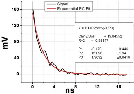
B tot 2-3 The second step in the calibration procedure was the internal resistance de-termination. In the Figure 2-4 the quenching part of a measured signal was se-lected. The exponential equation shown inside the box of Figure 2-4 was used to extract the decay time constant of the closed circuit of Figure 2-2B. Using the total capacitance value of 2-3 it is possible to extract the internal resistance of the diode. tot dC
R
T
P3
2-4Even if we know the sensing resistor value we can neglect this contribute because it is two order of magnitude smaller than the diode resistance and we are not sensitive to a so small value, that is inside in the experimental error.
Figure 2-4: Fit of pulse quenching shape.
The trend of the diode resistance, measured for various applied voltages, is noteworthy as shown in Figure 2-5. It appears that, for overvoltage values lower than 15% of the breakdown voltage, the junction is not fully activated and the
2.2 Calibration Measurements
29
resistance is greater than the constant value reached after 34 Volt. Starting from this consideration the internal diode resistance value can be calculated as the av-erage of the last four points of Figure 2-5, being the result:
]
[
07
,
0
42
,
1
/
C
K
T
R
d tot 2-5Figure 2-5: Measured diode internal resistance at various power voltages.
To evaluate the stray and diode contribute to the total capacitance we use the equation proposed by Cova in [12]:
s d d s E s
C
C
R
R
V
V
1
2-6This equation allows to calculate the maximum voltage amplitude of output signal Vs as function of diode and sensing resistors, stray and diode capacitances, and overvoltage vales VE=V-VB. From Eq. 2-6, and by approximating the capaci-tance configuration like a parallel connection, that means by neglecting the sens-ing resistor contribution, we can evaluate the equation of the stray capacitance:
tot s d E s s
C
R
R
V
V
C
2-7These equations show that the output maximum signal Vs is linearly depend-ent from applied overvoltage VE. This dependence is clearly shown in Figure
30
2-6. With the fit of experimental data plotted in Figure 2-6 we estimate the ratio
Vs/VE. Due to the fact that the threshold for the production of an output signal is
VE equal to Vb, the intersection with the horizontal axis is the breakdown voltage value.
]
[
2
30
5
,
1
7
,
29
V
V
B
A
V
V
B
B E s 2-8Even if the error in both measurement of the breakdown voltage shows a big uncertainty, the difference between the two values is four time smaller than the lowest measurement error.
Figure 2-6: Pulse amplitude versus power voltage.
Using Eq. 2-8 into Eq. 2-7 we obtain the stray and diode capacitance values:
]
[
09
,
0
14
,
1
]
[
09
,
0
21
,
0
pF
C
pF
C
s d 2-9The last unknown parameter of the system is the quenching process duration, represented by the time interval between the two transition of the two switch in Figure 2-1. This parameter do not have any influence on the signal production, but only achieves the truncation of the signal when it is practically zero, and triggers the start of the recharge of the system. So this value will be evaluated after the simulation of the output electric signal, pointing the time in which the current decreases below the latching current[12], when the overvoltage cannot ensure the avalanche process (section 1.3).
2.3 PQC with Ground on Cathode
31
2.3 PQC with Ground on Cathode
The PQC readout configuration is made with a sensing resistor on one side of the diode and the quenching resistor on the other side. The ground is com-monly pointed on the sensing resistor, to obtain signal on a base level equal to zero. Repeating the calibration procedure with the inverse configuration, with the quenching resistor on anode and sensing resistor on cathode, we obtain dif-ferent results that justify the difdif-ferent configuration shown in Figure 2-7. The reason of these differences is intrinsic of stray capacitance definition. Named the capacitance characteristic of a point to ground. In correspondence of the anode and the cathode of the diode we must consider two points that show capacitance characteristic toward the ground. On changing the ground configuration the stray capacitance connections and the capacitances configuration and values change, because the ground is moved to another position and, because the layers materi-als to ground change.
Figure 2-7: SPAD passive quenching configuration with ground on cathode side and full capacitance configuration.
32
Due to the small magnitude of the capacitance connected in series with the sensing resistor, it do not imply substantial signal modification and is not con-sidered in the simulation, as reported in circuital scheme of Figure 2-1. In pas-sive quenching configuration only the stray capacitance due to the junction semiconductor layer must be considered in the simulation. In conclusion the stray capacitances that must be considered in the simulation of the two passive quenching circuit configuration, of Figure 2-1 and Figure 2-7, are of different values and are located in different positions. To find the exact value of the in-verse configuration the calibration procedure should be repeated for the new configuration.
The second result of stray capacitance configuration is that not all the stray capacitances of the system contributes to the signal production. This second re-sult is enforced by the measurement shown in Figure 2-8 containing the fit of the system recharge trend (in red). The growing amplitude trend, that represent the voltage recharge shape, was fitted with an exponential trend. The time constant of the shape is related to the known resistivity of loop C of Figure 2-2 and the total capacitance of the system. The value evaluated with this fit is a bit larger than the total stray capacitance measured in the previous configurations.
0 1 2 3 4 5 0 10 20 30 40 50 60 70 Equation: y=A*(1-exp((T1-x)/T0)) Chi^2/DoF = 0.04254 R^2 = 0.99987 A 60.71201 ±0.10683 T0 0.03964 ±0.00323 T1 0.75962 ±0.00649 mV Time (us) Measure Exponential Fit
Figure 2-8: Voltage recovery of the PQC SPAD system made with a digital oscilloscope in persistent mode. The maximum voltage amplitude of the produced signals represents the recharge trend.
2.4 Comparison Between Measured and Simulated Signal
33
2.4 Comparison Between Measured and
Simulated Signal
Using the configuration of Figure 2-1 and the calibration results we are able to calculate the signal production. The comparison between the measured signal and the calculated one, by PSpice, is presented in Figure 2-9. While the ampli-tude and time decaying are in perfect agreement, the growth of the simulated signal is faster than the measured one, due to the time performance of the digital oscilloscope used to sample the signal. The bandwidth of the oscilloscope is 1GHz and the shown rise time is exactly one nanosecond, that is the maximum oscilloscope performance. Using a faster oscilloscope the mismatch will be re-duced. However the good agreement shows the validity of the electric SPAD model proposed and the goodness of the calibration procedure[21].
Figure 2-9: Comparison between measured and calculated pulse shape.
The characterization procedure developed and the explanation of the SPAD equivalent circuit for various configuration put us in the condition to design new approaches for the SPAD readout and for the two-dimensional matrix configura-tion, and also to specify the manufacturing objectives that can improve the per-formances of our application. In the analysis performed in chapter 5 we will un-derline the need of signals with fast rise time to improve timing performance,
34
with convenient amplitude to avoid the use of external amplification circuits, and with fast signal extinction in order to insert, inside a shared readout channel, a big number of produced signals and so a big number of SPAD devices.
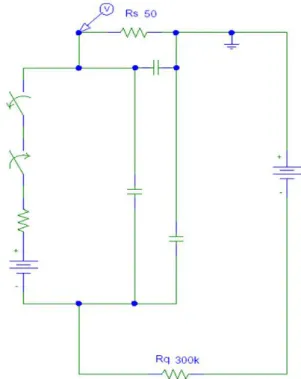
2.5 SPAD Double Readout
Configura-tion
As will be shown in the chapter 5, our readout strategy for two-dimensional imaging SPAD array needs two electric signals for each diode[22]. In the device used in this work the two signal are extracted one from the anode and the other from the cathode, as shown in Figure 2-10. The impedance of the front-end elec-tronics is 50 ohm, so to reproduce their behavior inside PSpice simulation only a 50 ohm resistor is needed. The anode front-end is represented by the resistor R-Anode located between anode and ground, while the cathode front-end is represented from the resistor R-Cathode connected to the cathode of the diode by the 5 pF a capacitor C-Decoupling.
2.5 SPAD Double Readout Configuration
35
The advantage of a simulation program is not only to test many configura-tions without losing time and without building real circuit, but, first of all, it is the ability to see how the circuit works collecting information that hardly can be extracted by a real device, and in addition with measurements that do not pro-duce any changes in the circuit, feature that is impossible to obtain in a real cir-cuit. Many simulation steps have been done to arrive to the final result presented in Figure 2-10, which takes into account the diode characterization, the availabil-ity of real electric component, and the virtual measurements done during the si-mulation.
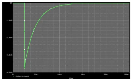
An interesting virtual measurement of the system is the current inside the di-ode. In the Figure 2-10 the closing time of the “on” switch is 10 ns, which simu-lates the photon adsorption. In Figure 2-11 this time represents the start of the current inside the diode. The switch closing rapidity can be chosen as one wants and, due to the high rapidity of the avalanche process, the faster value was cho-sen. When the switch is closed the discharge of the capacitances starts and the current value exponentially decreases. When the current decreases below, typi-cally, 0.1 mA, the avalanche multiplication process reaches a small value and the self sustaining process is no longer guaranteed. This is the time value to be used inside the off switch of Figure 2-10 to stop the avalanche. In the current shape this causes the current reset to zero value.
36
The anode readout configuration and the meaning of the signal produced was already shown in the diode characterization. The cathode readout can be done in different way. The system necessary for our imaging sensor must minimize the used components and the produced interferences. The performed simulated tests have shown that the use of a very small capacitor is the simplest way to obtain a cathode readout circuit. Choosing a capacitance we obtain an open circuit that do not perform any substantial variation in the current trip. The capacitance acts as a voltage decoupling that brings the background level of the produced signal from the applied voltage, typically 34 Volt, to ground level. The smallest com-mercial capacitance was chosen to reduce the increase of charge accumulation, that means a slower signal and a delayed recharge of the system. The produced signal is the derivative of the voltage shape in correspondence of the cathode. The calculated voltage shape in correspondence of the cathode is reported in Figure 2-12, while the produced signal after the voltage decoupling is reported in Figure 2-13 together with the anode produced signal.
2.5 SPAD Double Readout Configuration
37 Figure 2-13: Anode and cathode signals calculated with the simulation.
The sensor dead time can be also evaluated by measuring the recharge of the system. Changing the time scale of the Figure 2-12 it is possible to see the vol-tage recharge (Figure 2-14). The time scale of the produced signal is tens of ns while the recharge is in the µs scale. As shown in the diode characterization, the signal amplitude is linearly proportional to the applied voltage. So the recharge measurement is also important because represents the height of the signal pro-duced as function of the time delay from the previous signal, as reported in Fig-ure 2-8.
38
2.6 Array Configuration
Our two-dimensional array approach for imaging application well be deeply described in chapter 5. In this chapter we want to show some electric properties of our configuration. In the simulation we have paid attention on a reduced two-dimensional design of our device. A configuration with 6 diodes was simulated, configured in a two-dimensional array of three rows and two columns. In the Figure 2-15 the spatial position of the six SPADs is not designed to show the real spatial position of the diodes, but there is underlined the electric configura-tion of the system. The six diodes were posiconfigura-tioned along a straight line, on the top of the design there are two cathode line, while on the bottom there are three anode line. Each cathode line connects together the cathode of the three diode. Each group represents a column of the two-dimensional SPAD array. The ca-thode lines connect the diodes to the power source through the shared quenching resistors, and bring the signal to the decoupling capacitances. The two quenching resistors for the two columns are Rq1 and Rq2, while the two capacitances C1 and C2 together with the two resistor Rs1 and Rs2 represent the cathode readout channels. Near this two readout component the two stray capacitance Cs can be seen. In the bottom part of the design the three anode lines connect the two diode of each of the three rows. Inside each anode line there are three resistors, starting from the right, the sensing resistor Rs, the underpass resistors Ra, and the bulk resistors Rb. The bulk resistor connects the three lines but, due to its high value, its influence is negligible. The underpass resistor is a fabrication problem that will be discussed in the section 5.3. The first diode of the anode line is directly connected to the anode sensing resistor, the second diode is connected by the underpass resistor, the third diode, not shown in this reduced array configura-tion, will be connected through two underpass resistor, and so on. Each under-pass resistor causes a signal amplitude reduction that introduce a limit in the maximum number of diode in the same line. This limit will be deleted when the fabrication process will go to the next technology step.
2.6 Array Configuration
39 Figure 2-15: Electric schema of 3x2 two-dimensional SPAD array.
The proposed array simulation do not intend to calculate all the parasitic electric component that are located inside a real device. Only the measurement of real device can disclose the result of such complex interaction. However the proposed simulation, that takes into account the main characteristic of the elec-tric configuration, is able to show and to make understandable an unexpected ef-fects that we encountered in real device, the inverse electric cross talk. In corres-pondence of an anode signal produced by the adsorption of a photon a time cor-related signal was produced in the others anode readout channel. The amplitude of the subordinate signal is one order of magnitude lower and is of the opposite sign, which is useful to discriminate it. For this reason readout channel has been chosen to select only the signal produced with the right sign. In the electronic chain the anode real signal is positive, was inverted by an amplification with amplifier factor -1 and is read by a Constant Fraction Discriminator sensible on-ly to negative signal. In the Figure 2-16 there is shown the measurement of two anode channels after the amplification stage. The first channel (yellow) shows a little positive signal in correspondence of a true negative signal of the second channel (magenta). After few time the inverse situation occur, true signal on the first channel and false signal on the second channel. The simulation makes we
40
able to understand that this electric coupling is due to the capacity of the quiet diodes. The electric signal propagation is the same of that used for the cathode readout system. The junction capacity of the diodes connected each other by the same cathode contact, carries out the same effect of the decoupling capacity of the cathode readout system. So an inverse signal is produced on the other anode sensing resistor.
Figure 2-16: Simulated propagation of two signals inside the same anode metallization, and reflected signal on other anode channel.
2.7 Prototype: Binary Indexing
Rea-dout
In designing an imaging device two requirements must be fulfilled. The first is the spatial recognition of the fired pixel. The second is to increase the number of matrix elements with the smallest possible increase of necessary readout channels. Our imaging approach described in section 5.2 is an innovative solu-tion for indexing a square matrix with n2 elements, with 2n readout channel. As result of the collected experience in the electric design of simulated circuit we have produced another solution for the spatial recognition of the diode position.
2.7 Prototype: Binary Indexing Readout
41
Coupling the diodes with a different number of readout channels we obtain a binary word that identify the position of the diode. In Figure 2-17 we show a scheme for the reading of seven diode with only three readout channel. The readout scheme used is the same used for the cathode, already proposed in sec-tion 2.5, a coupling capacitor connected to a sensing resistor. The difference is that each diode is connected to a different set of sensing resistor. Starting from the right, the first three diodes are connected to only one resistor, the first diode to the first resistor, the second to the second and so on. Each of the three next diodes are connected to two sensing resistors, the first is not connected to the first resistor but is connected to the second and the third ones, the second diode is not connected to the second readout channel, and the third diode is not con-nected to the third readout channel.
In the simulation scheme we have decided to produce seven photon adsorp-tions, one for each of the seven diodes separated by 20 ns each other. The signal produced by this configuration is shown in Figure 2-18. The three colours used to emphasize the three readout channel of Figure 2-17 are also used to plot the three readout signals shown in Figure 2-18. The figure is clear for the first three produced signals, because each readout channel registers only one diode. The following three events are registered by two readout channels at the same time, so in the figure we obtain the pile up of two signals for each fired diode. De-pending on the printing order one colour is superimposed to the others. However the symbols coupled to the colour mark make visible the concurrent production of signals. The last signal is reported by all three readout channel, and the con-currence of the three symbols can be seen.
42
Figure 2-17: Row configuration with triple channel readout system for binary addressing for seven diodes.
2.7 Prototype: Binary Indexing Readout
43
for the capacitor. We decided to preserve the time characteristic of the seven diodes, so we decided to fix the total charge connected to each diode. The signal amplitude is proportional to the capacitance value. So if the diode is connected to only one readout channel only one capacitance is necessary, and the value is equal to the total capacitance available for one diode. If the signal must be pro-duced on two channels the total available capacitance must be shared for the two capacitances. In the last diode, where three signals are necessary, this value must be divided by three. In practice the amplitude of the signal produced is the same but it must be divided between the number of involved channels.
Figure 2-18: Signal produced in the binary indexing of seven diode into three readout channels.
In passive quenching circuit configuration of SPAD devices the signal am-plitude cannot be used to recognize the diode position, because this parameter is not fixed, but changes according to the recharge state of the diode. Instead, for SPAD with active quenching system the amplitude of the signal is fixed and can be statically selected to identify the position of diode that shares the same rea-dout channel. Adding together this two features, the binary indexing and the am-plitude recognition, we can multiply the number of diode per readout channel
44
and increase the imaging definition with a little increase of the device complexi-ty.
This two new approaches for array readout result from the simulation ap-proach and are not yet tested, but they can represent future device implementa-tions.
3. SPAD Counting
Correction
Since many years our research group is developing a Single Photon Ava-lanche Diode suitable for time resolved single photon imaging tech-niques[10][22][23][24].
In this chapter we describe how we developed a simulation code for the sta-tistical behavior of the SPAD. This code reproduces the behavior of the device under different illumination sources, taking into account its dead time and its noise production.
We study the signal generation process and the DT mechanisms of the de-vice. We start from the G-M studies present in Literature, and also analyze some effects, lacking in G-M counter, that should be introduced in the analysis of sem-iconductor device as afterpulse, reduced PDE and noise production.
We have used simulation code and dedicated experimental setup to verify each obtained results.
3.1 Simulation Technique
In the last years the simulation has became an important step of research process. The main impulse to this process is coming from the rapid growth of personal workstation computational performances, from new friendly access to large computational facilities, like INFN-GRID projects[25][26], and from the evolution of software dedicated to the simulation, like Matlab, PSpice, which we
46
used in this PhD work, or Comsol-Multiphysics, Opera, etc. All scientific areas take advantages from simulation, Physics, Chemistry, Engineering, Medicine, and, consequently, all innovation technology processes. The ability to predict the behavior of a mixture of well know effects, and vice versa, the ability to search combination of the fundamental rules that generates a well know effect, push the simulation process between the inductive and the deductive scientific research methods.
In the next subsections we show the simulation technique that we have de-veloped to verify results in SPAD dead time analysis (section 3.3) and to study the dead time effects on a sensor subjected to time dependent sources (chapter 4).
3.1.1 Light Source Simulation
The typical application for our counting device is the detection (time, posi-tion) of photons inside an acquisition time window. For statistic significance many time windows are acquired, and all data are merged into an histogram of the photon arriving times. Typical investigated light source is produced by a sys-tem excited by a rapid energy pulse that decades with a delayed light emission. By synchronizing the acquisition time window and the exciting pulse we obtain an histogram that shows the decaying trend.
The first step for the SPAD simulation is the developing of the photon source inside the time window. Starting from the simplest instance we will show how to produce a constant photon rate. After that we will add the step needed for the simulation of time modulated light sources.
Using a Poisson distribution we can decide how many photons to put inside each acquisition time window. The equation that describe the Poisson distribu-tion is: