Università degli Studi di Catania
Scuola Superiore di Catania
International PhD in Nanoscience
XXIV Cycle
Emission and amplification of light
from novel Si-based materials
Paolo Cardile
Tutor: Prof. Francesco Priolo
Cover
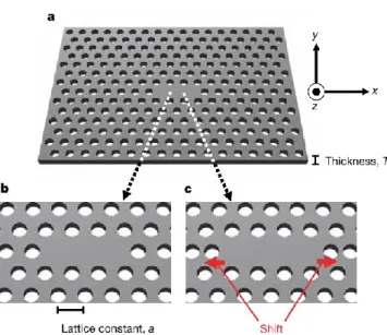
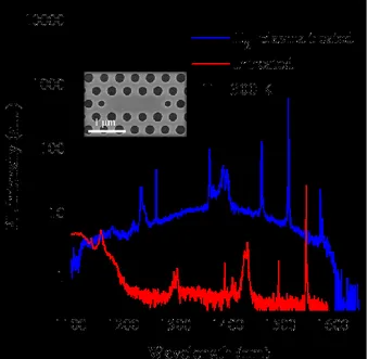
Top left: SEM picture of a photonic crystal, characterized by a triangular lattice. More details on the structural and electrical characterization of these artificial crystals can be found in section 3.3.
Top right: SEM picture of the electroluminescent device described in section 3.5. In the insets the image of the same device recorded by using an infrared camera in OFF and ON states are shown.
Bottom left: Schematic of the efficient quantum cutting process occurring in Y 2-xErxSi2O7 thin films. All the possible cross-relaxations are depicted. More details can be found in section 5.3.
Bottom right: Photoluminescence excitation spectroscopy performed on Yb2Si2O7, Y2-xErxSi2O7 and on Yb2-xErxSi2O7. More details on this subject can be found in sections 5.5 and 5.6.
Emission and amplification of light from novel Si-based materials
Paolo Cardile
PhD Thesis – Università degli studi di Catania – Scuola Superiore di Catania Printed in Catania – 5th December 2011
Wissenschaft ohne Religion ist lahm, Religion ohne Wissenschaft ist blind.
A. Einstein
La scienza senza la religione è zoppa, la religione senza la scienza è cieca.
Table of Contents
Chapter 1: Introduction
1
1.1
The fortune and the bottleneck of microelectronics 11.2
Content of this thesis 5References
7
Chapter 2: Photonic Crystals
9
2.1
Molding the flow of light 102.1.1 Maxwell equations and PhC 11
2.2
Photonic band structure in 2D PhC 152.2.1 2D PhC slabs and control of the spontaneous emission 18
2.3
Point defects in a PhC: nanocavities for photons 192.3.1 The Purcell effect 21
2.3.2 Ln cavities and gentle confinement effect 23
2.3.3 Heterostructure cavities 26
2.3.4 Local modulation of a line defect 29
2.3.5 Efficient light extraction out of a PhC cavity 31
2.4
PhC-based nanodevices 332.4.1 Slow light 33
2.4.2 2D PhC-based nanolasers 37
Chapter 3: Light emission from Si in PhC
nanostructures
45
3.1
Silicon. A bad emitter 463.1.1 How to get light out of Silicon 47
3.1.2 Luminescence centers in Silicon 50
3.2
H2-related defects obtained by plasma treatment 523.3
Electrical conduction across a PhC 633.3.1 Device fabrication 64
3.3.2 Electrical characterization 68
3.3.3 The depletion region 71
3.4
Quality factor of highly doped SOI PhC L3 nanocavities 763.5
Highly efficient electrically driven Si-based nanolight source 80Conclusions 85
References 87
Chapter 4: Light amplification in Er-based
materials
91
4.1
Optical fibers technology 924.2
Planar Si-based waveguides and amplifiers 974.3
Er-doping for planar amplifiers 994.3.1 Limitation of Erbium doping 101
4.3.2 Er-doped Si-compatible materials 106
Table of Contents
4.4.1 Y-Er mixed oxides 109
4.4.2 Er-based silicates 112
4.4.3 RE luminescence silicate: state-of-art 116
References 121
Chapter 5: Er compounds for optical amplifiers
125
5.1
Synthesis and structural properties of Y2-xErxSi2O7 thin films 1265.2
Optical properties of Y2-xErxSi2O7 thin films 1315.2.1 Correlation between structural and optical properties 132
5.2.2 Photoluminescence from Er in -Y2-xErxSi2O7 136
5.3
Er-Er interactions in Y2-xErxSi2O7 1385.3.1 Influence of Er concentration on the emission
from Y2-xErxSi2O7 139
5.3.2 Quantum cutting effect 142
5.3.3 Cooperative upconversion 149
5.4
The effect of Yb sensitization: synthesis and structuralproperties of Yb2-xErxSi2O7 thin films 154
5.4.1 Elemental characterization of the Yb2-xErxSi2O7 films 155
5.4.2 Crystallization properties of Yb2-xErxSi2O7 thin films 159
5.5
Optical properties of Yb2-xErxSi2O7 thin films 1615.6
Er sensitization by Yb ions 1645.6.1 Sensitization of Er3+ through Yb3+ ions: energy transfer
between the two rare earths 164
5.6.3 Comparison between the two rare earth silicates for optical amplifiers 170 Conclusions 172 References 175
List of publications
179
Acknowledgements
183
____________________________________________________________________
1. Introduction
1.1 The fortune and the bottleneck of microelectronics
The fortune of microelectronics since its birth to nowadays is certainly due to Moore’s Law, regulating the progressive miniaturization [1]: since the sixties of the last century, starting from the invention of the first transistor, in fact, a growing number of devices were implemented in the same silicon chip, by reducing continuously their size, with the aim of reducing the production costs and of increasing the performances of the chips.
The advances we assisted in the last fifty years allow now to have faster, smaller and cheaper microprocessors, thus improving remarkably the performances of our computers. This is the nanotechnology era, which deeply changed our daily life, since it gave us portable laptops or smart phones, permitting us to be connected to the world everywhere at any time.
The high performances of our modern devices are ruled not only by the miniaturization, but also by the multi-core systems. In fact, over the last three decades, the microprocessor performances scaled from devices that could perform tens of thousands of instructions per second to tens of billions of instructions per second in today’s products. The architectures inside the microprocessors had to be changed, moving both towards the miniaturization of the single device and towards parallel cores, working together to improve the performances. Thanks to these multi-core systems, now we are approaching the era of Tera-scale computing. The next goal of a big company, like Intel, is in fact the realization of 10 Tera-instructions per second by 2015.
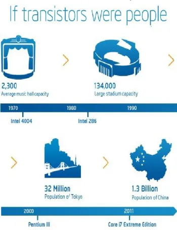
A particular representation of the recent progress of microelectronics is reported in fig. 1.1. Suppose that the number of components or transistors inside a microprocessor is represented by people. We can associate this number (as it was in 1970) to the people that can be placed in a big music hall, 2300 people. With time, the number grows more and more: year by year the population becomes too large and has to be inserted in a large
stadium (1990) or in a big city like Tokyo (2000). Today we can imagine that the population is of the order of the Chinese one (about 1.3 billion inhabitants). Now suppose that all of these people are still confined in the original music hall. This gives the idea of the progressive scaling down of the device size during the decades. In fact the number of transistors in a chip increased by seven orders of magnitude, while the minimal feature of lithographic design has been reduced from 30 m to 16 nm and this is the reason why we talk about nanoelectronics, nowadays.
Figure 1.1: Miniaturization during the last forty years, according to the developments obtained by Intel. Adapted from [2].
However, as a consequence of the continuous reduction in size, much longer electrical connections are required in order to let all the components talk each other, and at a larger scale to link different microprocessors integrated in the same circuit board. The total length of the metallic
Chapter 1 – Introduction
interconnections is now of the order of 10 km in a micrometric area and therefore the wired network is so complicated that many levels of metal are required. This dramatic increase of the total length of the metallic circuitry leads to a consequent huge increase of signal delays, signal cross-talks and electromagnetic interferences causing power dissipation. This is the most important limitation for further developments.
Therefore the entire scientific community defines this problem as an electronic bottleneck, because soon it will be very hard to further reduce the minimal feature size.
A possible solution to this problem is represented by replacing the electrical interconnections with optical ones for linking chip-to-chip and board-to-board [3]. Photons, in fact, do not suffer the same problems of the metallic connections, having the possibility to travel at the light speed in the medium they pass through.
Figure 1.2: Schematic picture of an ideal optoelectronic device, in which optical and electrical elements cooperate in a single chip [3].
The success of optical fibers in long-range communications started off the research in the micrometric photonic circuitry. As it happens for the long-haul communication system, also at the micrometric scale the basic components necessary to have an optical network are a light source (a laser), a channel for carrying information (waveguides), a detector, a modulator of the signal. These devices must be integrated together in the same substrate in
order to cooperate and make a working circuit, as depicted in fig. 1.2: this is the dream of integrated photonics. However these devices usually require different materials in order to optimize their functions, namely the generation, the control and the detection of photons.
The most common materials are direct band gap III-V or II-VI semiconductors for light emission and other materials, such as lithium niobate, for modulation, and they are not fully compatible with the Silicon technology. The realization of these components with Si-compatible materials is a very important issue, since this can provide a remarkable reduction of the production costs, the achievement of global diffusion and a compatibility with the electronic devices, which are currently integrated into the Silicon chips.
Nowadays the fabrication of passive devices, such as waveguides, splitters or multiplexers, is well developed on Silicon. However a necessary step forward is certainly the realization of active devices, like a laser, which is an efficient and coherent light source, or an optical amplifier.
Lasers and amplifiers are fundamental components and they are important for two independent reasons: the former is the generation of light-dark signals that can be associated to the logic values 1-0; the latter is the compensation of optical losses when light passes through passive components. Unfortunately Silicon is not an efficient light emitter, and this is a limitation that is hard to be overcome. Despite the achievement of optical gain [4, 5] or of a Raman-based stimulated emission [6, 7], a proper electrically-driven Silicon laser is still lacking. Some III-V nanolasers [8-11] are claimed to be the solution to the problem, since they can be actually grown on a Si substrate. However this is not going to be pursued by the current society, since the idea of making every optoelectronic device with Silicon is still the (cheapest and the) most fascinating.
Therefore it is necessary to find efficient strategies, in order to achieve the realization of new efficient active devices compatible with the Si-based technology: this is the object of this thesis.
Chapter 1 – Introduction
1.2 Content of this thesis
The aim of this thesis is to study in detail novel Silicon-based nanostructured materials which allow to obtain the emission and the amplification of infrared light. In both fields we achieved interesting results: by using the advantages of Photonic Crystals, a prototype electroluminescent device is presented, with the highest spectral density and the lowest linewidth ever measured for Silicon at room temperature and at telecommunications wavelengths. Moreover, by exploiting the advantages of the rare earth compounds, a promising material is proposed for the realization of an optical planar amplifier.
The thesis is organized as follows:
In Chapter 2 the physics of Photonic Crystals (PhC) will be introduced. These “artificial crystals” are characterized by a periodic distribution of the refractive index and were proposed in the late eighties of the last century. In this chapter the properties of PhC are described in detail by using Maxwell equations. It will be shown that PhC can efficiently control the propagation of light in the periodically patterned structure, acting with photons similarly to how the solid state crystals do with electrons. They can guide light and they can be used to realize cavities, in which light is trapped, travelling forward and backward. We present the ultimate ultra-high Q factor cavities that can be found in the recent literature, showing the advantages of different approaches in the design. In these cavities, which are actually cavities at the nanometer scale, it is possible to control also the spontaneous emission of an emitter placed inside them. This is the Purcell effect and it will be shown how it can be used for. Some recent PhC-based devices are also reported, showing that the many properties of the PhC can be used for third-harmonic generation or for the achievement of low-threshold lasing.
Chapter 3 will show how it is possible to obtain efficient light
emission from nanopatterned Silicon. During the fabrication of SOI wafers, in fact, some defects are introduced by Hydrogen implantation. These defects are optically active and their photoluminescence can be extracted
with a PhC structure. By treating the samples with a Hydrogen-rich plasma, a much stronger photoluminescence is obtained. This is due to a passivation of the Silicon surface and to the introduction of a further amount of defects in the Silicon slab. A discussion on the electrical conduction across a Photonic Crystals is then reported and finally the fabrication of the most efficient electrically-driven nanolight source in Silicon ever registered is described. This source works at room temperature and at telecommunication wavelengths. The measured linewidth and the spectral density of our light emitting device are seriously comparable with those of III-V nanolasers, working at cryogenic temperatures. We believe that this is going to be a milestone in the future story of Si-based photonics.
On the other hand, the second part of the thesis will be focused on the light amplification at 1.54 m, by making use of erbium, a rare earth ion that is characterized by a radiative transition exactly at this wavelength.
In Chapter 4 it will be discussed why this wavelength (and erbium, consequently) is so important and at the same time all the problems of incorporating erbium in a silicon based material will be reviewed. Among these problems, clustering and Er-Er interactions are described in detail. A strategy to improves the number of optically active Er ions is reported, by making use of Er compounds, such as oxides and silicates, in which the Er concentration can be varied continuously from the typical dopant regimes (~1019 Er/cm3) up to the compound values (~1022 Er/cm3).
In Chapter 5, the last chapter, it will be shown how it is possible to incorporate a large amount of erbium in Er-based materials, namely Y-Er disilicate and Yb-Er disilicate, grown by sputtering. These materials are studied in detail, by performing a complex structural characterization, with Rutherford Backscattering Spectrometry and X-ray Diffraction Analyses. The optical properties of these materials are also studied extensively. We demonstrate that Y-Er silicate is a very interesting material with good properties for applications in photovoltaics, being characterized by the occurrence of a quantum cutting phenomenon. Yb-Er disilicate, on the other hand, is more advantageous for light amplification at 1.54 m. In this compound a strong energy transfer from Yb to Er is demonstrated, with noticeable efficiencies. This silicate is in fact proposed as a very promising material for realizing a planar amplifier onto a Silicon substrate.
Chapter 1 – Introduction
References
[1] G. E. Moore, Electronics 38 (1965). [2] Intel website www.intel.com
[3] M. Paniccia and S. Koehl, IEEE Spectrum 42, 38 (2005).
[4] S. G. Cloutier, P. A. Kossyrev and J. Xu, Nat. Mater. 4, 887 (2005). [5] L. Pavesi, L. Dal Negro, C. Mazzoleni, G. Franzò and F. Priolo, Nature
408, 440 (2000).
[6] H. Rong, A. Liu, R. Jones, O. Cohen, D. Hak, R. Nicolaescu, A. Fang and M. Paniccia, Nature 433, 292 (2005).
[7] H. Rong, R. Jones, A. Liu, O. Cohen, D. Hak, A. Fang and M. Paniccia, Nature 433, 725 (2005).
[8] H. Altug, D. Englund and J. Vuckovic, Nature Phys. 2, 484 (2006). [9] A. Tandaechanurat, S. Ishida, D. Guimard, M. Nomura, S. Iwamoto and I. Arakawa, Nature Phot. 5, 91 (2010).
[10] B. Ellis, M. A. Mayer, G. Shambat, T. Sarmiento, J. Harris, E. E. Haller and J. Vuckovic, Nature Phot. 5, 297 (2011).
[11] R. Chen, T.-T. D. Tran, K. W. Ng, W. S. Ko, L. C. Chuang, F. G. Sedgwick and C. Chang-Hasnain, Nature Phot. 5, 170 (2011).
____________________________________________________________________
2. Photonic crystals
Photonic crystals are artificial structures in which photons behave as electrons do in a solid state crystal. They are characterized by a periodic distribution of the refractive index in one, two or three dimensions. It has been demonstrated that it is actually possible to engineer these structures, in order to have a complete control of light. The equations regulating this property are Maxwell equations solved in this particular periodic medium.
By considering the analogy between electrons in a solid and photons in a photonic crystal, it is easy to understand the existence of a photonic band gap and all the properties coming from it. One of the most interesting effects regards the control of the spontaneous emission from two-dimensional photonic crystal slabs, and this is well exploited in many applications.
A further control of the spontaneous emission rate is achieved by realizing photonic crystal nanocavities: these cavities are characterized by a very high Q factor and a very small mode volume, thus being very promising for the occurrence of a strong Purcell effect, which significantly enhances the spontaneous emission rate.
It is possible to engineer the cavities, simply by modifying the local geometry of the photonic crystals. Therefore it is possible to have either a higher Q factor by gently confining the optical mode in the cavity or to have a stronger out-of-plane coupling, in order to optimize the light emission of a photonic crystal device. In any case a slight modification of the geometry is required, meaning that photonic crystals are very versatile for different kind of applications. Additionally some other properties of photonic crystal waveguides can be used, like the slow light effect, which increases the light-matter interaction by orders of magnitude, thus enhancing non linear effects like visible third harmonic generation in Silicon.
Finally some photonic crystals-based lasers can be realized with low lasing threshold and very high modulation rates. All these lasers generally work with III-V semiconductors. The new challenge is then to demonstrate an efficient light source in silicon. Are photonic crystals the right way to pursue this goal?
2.1 Molding the flow of light
One of the most fascinating subjects of the research in photonics during the last decades concerns the complete control of light by making use of Photonic Crystals (PhC). A crystal is a spatial arrangement of atoms, placed in well-defined position in a periodic way, according to specific patterns, called crystal lattices. A lattice is actually an infinite array of discrete points which appears to be exactly the same from whichever of the points the array is viewed. From the Quantum Mechanics point of view, it is possible to treat such crystals as periodic distributions of the Coulomb potential: this explains why electrons in a perfect crystal know exactly how to move, without hurting any atom in the lattice, being interpreted like waves.
Moreover the solid state semiconductor lattices can also forbid the propagation of some particular electronic waves. In fact by considering their dispersion relation, i.e. the function linking energy and momentum of electrons, some “electronic states” can be actually prohibited. These are the so-called semiconductor energy gaps, which separate the valence band and the conduction band and define an ensemble of forbidden electronic states. For Silicon, for instance, the diamond-like lattice allows to have an energy gap about 1.1 eV large at room temperature.
The deep knowledge of solid state physics allowed to perfectly understand how to control the electrical properties of semiconductors, thus opening the route to a progressive development in the microelectronic technology. Therefore in the eighties of the last century a new interesting idea came out, answering the question: is it possible to realize artificial materials in which photons are subjected to similar laws than those of electrons in crystals? In other words, is it possible to perfectly control the light propagation in a certain material? The answer is yes, as it will be discussed. Photonic crystals, in fact, do to photons what semiconductor crystals do to electrons, creating a situation in which photonic modes are not permitted [1].
Chapter 2 – Photonic Crystals 2.1.1 Maxwell equations and PhC
In a PhC the periodic atomic Coulomb potential is replaced by a periodic dielectric function. In order to solve this problem from a mathematical point of view, it is possible to use Maxwell equations, instead of Quantum Mechanics. In fact Maxwell equations perfectly describe a physical system in which there is a defined distribution of dielectric functions. In the particular case of photonic crystals, this distribution is periodic, and it involves two media with a sufficient difference in the refractive index (i.e. in the dielectric constant).
The dielectric unit can be repeated either in one dimension (the quarter-wave stacks, for instance) or in two dimensions (the most used photonic crystals), or even in three dimensions (a woodpile structure is a famous artificial example, while opals are the most known three dimensional PhC existing in nature), as depicted in fig. 2.1.
Figure 2.1: Pictures of different periodic structures in one, two or three dimensions [2].
The local Maxwell equations in a medium, expressed for each point in the space and for each instant, are well known [2, 3] and are here reported:
(2.1)
0
ρ
t
t
B
D
D
H J
B
E
where E and H are the microscopic electric and magnetic fields, D and B are the displacement and the magnetic induction fields, and finally and J are the free charges and the current densities. We will consider the propagation in a mixed dielectric medium, whose structure does not vary with time and, without any sources ( and J=0). Moreover we will consider the simplest relation of proportionality between D and E and between B and H, assuming that the material is isotropic, without any dispersion, and transparent. In this specific case, we have that D(r) =
0 (r)E(r) and B(r) = 0 (r)H(r).
For almost all the dielectrics of interest, however, (r) = 1. By considering all these assumptions, it is possible to re-write the equations in the following way:
(2.2)
In general, the electric and the magnetic fields are complex functions of space and time. However, since the equations are linear, it is possible to separate the time dependence from space, by expanding the fields in harmonic modes. This is not a limitation, because it is known from the Fourier analysis that any function can be written as a linear combination of these modes. Therefore, by using the complex exponentials:
(2.3) and by substituting them into Eq. (2.2), we obtain for the first two equations:
(2.4)
These results mean that there are no sources in the material, either electric or magnetic. If the fields are plane waves, i.e. if the dependence on
0 0
( , t) = 0
(ε( ) ( , t)) = 0
( , t)
( , t) = ε ε( )
t
( , t)
( , t) = μ
.
t
Η r
r E r
E r
H r
r
H r
E r
( , t) = ( )
( , t) = ( )
i t i te
e
H r
H r
E r
E r
( ) = 0
(ε( ) ( , t)) = 0
H r
r E r
Chapter 2 – Photonic Crystals
the space is H(r) = a exp(ik∙r), then it means that the fields are transverse. The other curl equations, on the other hand, become:
(2.5) mutually relating the electric field and the magnetic one. It is possible however to decouple them, by dividing the first equation by (r) and by applying again the curl. In this way, by using also the second equation, it is possible to eliminate the electric field. Given that 0 0 = 1/c2, being c the
light speed in the vacuum, we thus obtain:
(2.6) This is the so-called master equation and it describes the behavior of the magnetic field. For a given (r), the master equation can be solved, thus finding the modes H(r) and the corresponding frequencies, by taking care of the transversality condition. After that it is possible to find also E(r), just by taking the curl of H(r) according to Eq. (2.5). In this case, however, E(r) is already transversal, since it is expressed as the curl of H(r), and the divergence of a curl is always zero.
This is a general discussion, arising just from generic considerations about a medium in which light is propagating. In the specific case of the photonic crystals, we already said that the refractive index is distributed in a periodic way. In other words, the dielectric function (r) is a periodic function of r. Let us have a look again at Eq. (2.6): the first term is nothing but an operator for the magnetic field: it consists in a curl, a multiplication and another curl. If the dielectric function is periodic, this operator keeps the spatial periodicity of (r), thus being a periodic operator. Therefore we can see that the master equation is analogous to the Schrödinger equation for the electrons in a crystal: (2.7) 0 0
( ) = ωε ε( ) ( )
( ) = ωμ ( )
i
i
H r
r E r
E r
H r
21
( ) =
ω
( ).
ε( )
r
H r
c
H r
2 2h
V( ) ψ( ) = E ψ( )
2m
r
r
r
where ψ is the electronic wave function, the first term in parenthesis is the kinetic energy operator, while V(r) is the periodic Coulomb potential. Note that solving the master equation is an eigenvalue problem, similar to that of Quantum Mechanics. The analogy is complete since, both for electrons and light, the eigenvalues are energies1. For the photons, these eigenvalues are
the frequencies of the electromagnetic field, and the eigenfunctions are the fields themselves.
There are two main differences however: the first is that there is not any quantistic effect in the propagation of photons in a periodic medium. It is just a classical physical effect, though the mathematics lying beyond is similar. The second is that the master equation is scale invariant and this property comes from Maxwell equations: there is no a fundamental length scale and this is very important from the practical point of view. In fact it is always possible to rescale the system in order to have a certain eigenvalue [2].
All the solutions of the Schrödinger equation as a function of the momentum vector of the wave function permit to construct the band structure of the solid under investigation. From the same equations it is possible to justify the existence of the energy band gap for semiconductors and insulators. As it happens for semiconductors, this behavior can be seen also for photonic crystals. This property provides the opportunity to shape and mould the flow of light for photonic information technology.
By properly adjusting the photonic crystal structure, it is then possible to obtain a certain range of wavelengths for which photons cannot propagate in a photonic crystal. The existence of such photonic band gap materials in 3D was demonstrated in the early nineties [4-6], and the first experimental proof was found by using an array of holes drilled into a high refractive index material [6]. That centimetre-scale face-centred cubic artificial crystal, known also as Yablonovite2, showed a stop band for the transmission of
microwave radiation from 13 to 16 GHz, independently of the direction. Later on, the first structures working in the near IR (between 1.35 m and 1.95 m) were also demonstrated [7].
1 Note that in the master equation, is an energy divided by ħ. 2 After the name of its inventor E. Yablonovitch.
Chapter 2 – Photonic Crystals
Recently lasing was shown from a III-V semiconductors-based woodpile structure, i.e. an alternate sequence of GaAs thin layers (each containing line and space), with InAs quantum dots as active medium [8].
On the other hand, 2D PhC structures are much more interesting and we will show them in more details. The reason is that 2D artificial crystals are much easier to be fabricated, in particular thanks to the development of lithography and etching techniques. Additionally, lower dimensionality helps in modifying the crystals (for instance introducing defects deliberately) or in interfacing the PhC to any microphotonic device.
2.2 Photonic band structure in 2D PhC
A two dimensional PhC is characterized by an in-plane periodicity of the refractive index and by a light confinement in the third dimension, like a quantum well for electrons. A 2D PhC can be realized by making holes in a semiconductor material, by using electron beam lithography and a strong directional etching technique with high resolution. Such a material is then a sequence of ordered holes that can be arranged as reported in fig. 2.2, representing a schematic of a triangular lattice with a lattice parameter a and a hole radius r [2]; a SEM picture of the same lattice designed in AlGaAs is also shown [9].
Figure 2.2: Example of two-dimensional PhC with a triangular lattice [2]. An SEM picture, showing the first attempt of using this lattice in AlGaAs is also reported [9].
In the case of 2D PhC, the master equation can be solved and the eigenfunction are characterized by the wave vector k and by a band index n, therefore we identify the modes as n(k). Sometimes the frequency is
The comparison of two different lattices from the band gap point of view is reported in fig. 2.3. The top panel is the band structure of a square lattice of alumina rods ( = 8.9), surrounded by air ( = 1.0). The rods have a diameter of 0.74 mm and a length of 100 mm and are arranged in a square array with lattice constant a = 1.87 mm. This band structure was calculated (continuous lines in the graph) and experimentally measured (square points). The x axis shows the values of the in-plane wave vector k||. Note that in the x
axis some specific points are indicated: , X, M. They correspond to the directions in the lattice k|| = 0, k|| = /a , and k|| = /a + /a .
Figure 2.3: Band structure of an array of alumina columns surrounded by air in a square lattice distribution (top panel) and of a triangular lattice with holes of air in a dielectric (bottom panel) [10].
Chapter 2 – Photonic Crystals
For both the components of the electromagnetic field, namely the transverse electric (TE) and the transverse magnetic (TM) modes3, there is a
perfect agreement between experiment and theory. Moreover it is clear that only for TM modes there is the existence of a large photonic band gap between the first band and the second one. This does not happen for TE modes. In fact, for the lowest TM band, the field is concentrated in the dielectric regions, while for the second band, it is concentrated in the air regions. By considered k fixed, for instance at the X point, the two associated frequencies are therefore noticeably splitted.
On the contrary, for the TE case, both the low band and the top band modes are significantly placed in the air, with a high frequency. This fact can be explained by considerations regarding the distribution of energy coming from Maxwell equations [2]. Exactly the opposite behavior is seen for a connected dielectric square lattice. Therefore TM band gaps are favoured in a lattice of isolated high- regions and TE gaps are favoured in a connected high- lattice.
In order to have a complete band gap photonic crystal, it is necessary to make a compromise on the geometry: the crystal needs to be connected but at the same time the high- regions must be practically isolated. An example of this system is the triangular lattice of air columns, as that shown in fig. 2.2. In fact for this system the band structure reported in fig. 2.3 (bottom panel) has a complete band gap for both TE and TM polarizations. In the region highlighted in yellow, where a/2 c is between 0.4 and 0.5, light cannot propagate in the medium, whatever is its propagation direction
k.
Besides the lattice configuration, the other main factor that determines the properties of the band gap of a 2D PhC is the refractive index contrast. In general, the higher the refractive index contrast, the larger the band gap achievable.
3 TE (TM) means that there is no electric (magnetic) field in the direction of
2.2.1 2D PhC slabs and control of the spontaneous emission
In this section we will show how it is important the existence of a photonic band gap (we will call it PBG, for the sake of simplicity).
In a two dimensional photonic crystal, light propagation in the orthogonal direction (with respect to the 2D periodicity) cannot be controlled by the photonic band gap effect, because no periodicity is registered in that direction. In order to use this dimensionality for feasible applications, a thin slab structure was suggested. This slab is a freestanding membrane being surrounded by air (or another low-index dielectric, eventually) and it is realized in order to achieve a strong optical confinement in the vertical direction.
Figure 2.4: (a) SEM picture of a GaInAsP 2D photonic crystal slab. A 5 nm QW layer is inserted in the middle of the slab, being the active emitting layer. (b) Emission spectra for samples with lattice constant between 350 and 500 nm. The blue region denotes the PBG. (c) Time-resolved measurements for all the samples investigated. [11, 12].
Chapter 2 – Photonic Crystals
Owing to this property it was demonstrated that such slabs successfully manage the manipulation of light, by controlling in particular spontaneous emission [11]. Noda and coworkers fabricated a GaInAsP 2D PhC slab (245 nm thick) structure with a single quantum well (QW) light emitting layer, as reported in the SEM pictures in fig. 2.4 (a) [12].
Many samples with the same triangular lattice but with a different lattice parameter a were realized. In all cases the holes radius is r = 0.29a. As shown in fig. 2.4 (b) the photonic band gap (denoted as PBG) shifts to larger wavelengths by increasing a. The lifetime of the excited carriers are also reported in panel (c) of the same figure. When the emission wavelength is inside the band gap (a = 390 – 480 nm) the lifetime increases (i.e. the emission probability decreases) compared with the lifetime without the PBG effect. At the same time the vertical emission peak increases significantly (see fig. 2.4 (b)). Therefore this particular geometry was remarkably able to reduce the in-plane spontaneous emission rate, while the light extraction in the vertical direction was enhanced. Therefore when the spontaneous emission is inhibited by the PBG effect, the energy is saved and re-distributed in other mechanisms, such as the emission out-of-plane. This effect is very useful for many applications in photonics, such as illuminations or solar cells.
We can then conclude that a PhC slab is able itself to inhibit spontaneous emission, just because of its PBG. Recent experiments have demonstrated that it is possible to suppress spontaneous emission by roughly the theoretical limit (~15 times) [13].
2.3 Point defects in a PhC: nanocavities for photons
It is well known for semiconductors that, once point defects are inserted in the lattice, new states appear in the semiconductor band gap, associated to the breaking of the symmetry in some points of the crystal. This behaviour can be seen also for photonic crystals. The perturbation of a point defect, deliberately introduced in the artificial crystal, is responsible of the creation of localized modes, having a frequency in the forbidden band gap. This perturbation can be realized for instance by changing the dielectric constant of a column in a PhC realized by identical columns surrounded by
air. Another possible configuration is realized by avoiding to make holes in a lithographically defined PhC, in which columns of air are etched down in a semiconductor.
The as-created photonic mode cannot propagate in the rest of the crystal, because there it falls inside the band gap: therefore this defect-related mode is spatially localized where the physical defect lies. So the mode decays exponentially and evanescently out of the defect. These modes are localized in the xy plane, and they are extended in z. The boundaries of the defect actually act as mirrors and therefore the point defect is nothing but a cavity for the photons, because light cannot escape from it.
The two most important features of a cavity are the Q factor, that is the energy loss per cycle divided by the energy stored inside, and the modal volume Veff, i.e. a measure of the spatial extent and energy density of the
mode. The Q factor represents how strong is the confinement inside the cavity.
Light confinement in a generic photonic cavity is a very important topic for several applications, since it can enhance the electron-photon interaction [14] or non linear optics [15] or the occurrence of other quantum effects, useful for quantum information technology [16]. Very high Q factors (of the order of ~108) were measured in micrometric ring resonators [17], but
in that case the dimension of the ring is much larger than the wavelengths used. Photonic crystals are very interesting because they can offer a very high Q with very small modal volumes, of the order of a cubic half-wavelength in the host material. Therefore they allow to strongly reduce the dimension of the cavity, without suffering scattering losses, as it would happen by scaling down the dimension of a microring.
Fig. 2.5 reports two SEM pictures: one is referred to a silica microring resonator with a 108 Q factor [17], while the second is a PhC cavity [18].
They are reported together in order to see effectively from the markers which is their difference in size. This particular PhC cavity is realized in InAsP by grading the size of the holes in order to induce the formation of a point defect in the crystal. This was the first demonstration that the Q factor of PhC cavities can be in excess of 104 [18].
Chapter 2 – Photonic Crystals
Figure 2.5: SEM pictures representing a ultra-high Q microring resonator [17] and a PhC cavity [18]. Note the difference of the two markers.
At a first glance it would seems that microrings are much more efficient cavities. On the other hand the mode volume in the case of PhC is much smaller. This is crucial, because the ratio Q/Veff determines the
strength of the various cavity interactions, as it will be pointed out later. In this case, PhC cavities work better than microring resonators and, being very small, they enable large-scale integration.
2.3.1 The Purcell effect
We have seen previously that the PBG can itself provide a control of the spontaneous emission rate. However another fundamental and more powerful mechanism that is able to control spontaneous emission is the Purcell effect. This effect can be observed when an excited atom is put inside a photonic cavity [19]. In order to explain this effect, let us start from its definition: spontaneous emission occurs when an emitter relaxes from one of its excited states to its ground state, by photon emission into an optical mode that is not occupied by another photon. The rate of this process is determined by Quantum Mechanics, and in particular by using the framework of the Fermi’s golden rule, which can be expressed as:
(2.8)
being Γi,f the transition probability that the system in an initial state i
moved to a final state f , thanks to the interaction term of the Hamiltonian 2
, i
2π
ˆ
=
H
ρ(ω)
describing the system, Ĥi. The last term, ( ), is the density of the final
states, the number of states per unit of energy and it depends on the energy (or on the frequency separating the initial and the final states). This equation comes from the time-dependent perturbation theory in Quantum Mechanics.
Unfortunately, spontaneous emission is in many cases troublesome, since it limits the performance of many devices. For instance, lasers are coherent light sources and when in the active medium a spontaneous emission is not coupled to the lasing modes the lasing threshold becomes higher and there is also some undesired noise. These problems are the basis of the research on how to control and manipulate spontaneous emission in photonic crystals-based systems. We will show now how a photonic cavity can do this.
The volume-normalized mode density g( ) (that is ( )/V) is proportional to 2, according to [20]:
(2.9)
If the emitting atom is in resonance with the cavity, and if the linewidth of the emitter is entirely inside the cavity resonance, then the cavity restricts the modes to a spectral width and a volume Vcav and the
density (in the case of Lorentzian shape) can be written as:
(2.10)
On the other hand the cavity is characterized by a quality factor Q, which can be written as Q = . By substituting it in Eq. (2.10), we get:
(2.11) Therefore the mode density alteration caused by the cavity is given by the ratio gc/gf, that is:
(2.12) 2 f 2 3
ω
g (ω)
.
π c
c2 1
g (ω)
.
π ΔωV
c2Q
g (ω)
.
πωV
2 3 3 3 c 2 3 2 fg
2Q π c
2πc
Q
λ
Q.
g
πωV ω
ω V
4π V
Chapter 2 – Photonic Crystals
The maximum enhancement can be obtained if the emitting radiative dipole is oriented to have the strongest interaction with the cavity mode and this gives an additional factor 3. The enhancement factor, fP, known also as
Purcell factor, can be therefore written as:
(2.13)
This shows that this factor, enhancing the spontaneous emission rate, is proportional to the ratio of Q factor divided by the cavity mode volume, meaning that PhC can be very promising in this field, having both a high Q and very small volume. Note that, with respect to the best ring resonators [17], PhC nanocavities can show a Q/V factor even two orders of magnitude larger [21-25], thanks to new and efficient designs.
Recently it was experimentally demonstrated that a relatively high fP
can reduce by orders of magnitude the lasing threshold, and this happened in different systems [26-28], but still not in the most important platform, that is Silicon of course. For Silicon, PhC cavities can be realized by using a Silicon-On-Insulator (SOI) wafer: with this kind of support, it is easy to realize slabs, since, after the etching of the holes in the silicon layer (about 200 nm thick), it is possible to membrane the PhC pattern, by means of chemical wet etching. We will show next how to fabricate some examples of PhC nanocavities, allowing a better and better confinement, namely Ln
cavities (in particular L3 with gentle confinement effect), heterostructure
cavities, and cavities with local modulation of the holes in a line-defect.
2.3.2 Ln cavities and gentle confinement effect
Ln cavities are realized by removing n holes in the -K direction in a
triangular lattice of a PhC slab. In this particular case, by considering a perfect 2D crystal, the lacking of this n holes allows some states inside the band gap. This is the perturbation in the perfect repetition of the dielectric unit constituting the PhC cavity. Advance design techniques actually brought to the realization of different geometries of PhC cavities, in order to achieve a better and better Q/V ratio, thus candidating them for applications in large-scaled devices. 3 P 2
3λ
f
Q.
4π V
Figure 2.6: 2D PhC cavities realized by using a slab. (a) Schematic of the triangular lattice. (b) Starting cavity with three missing holes in the -K direction and (c) cavity with the holes displaced at both edges [25].
An example of Ln cavities is shown in fig. 2.6 for n = 3: in this scheme
an L3 cavity is depicted, realized in a SOI-based PhC 250 nm thick slab. In
this case just 3 holes are missing in the lattice, which is characterized by a = 420 nm and by a holes radius r = 120 nm [25]. With these parameters, the cavity is working around the telecommunication wavelength of 1.5 m.
In this situation, the physical mechanism of total internal reflection (TIR), which works well in the description of microcavities, has to be reconsidered, since the photonic nanocavity has the dimension of the same order of magnitude of the wavelength. When light is confined in such small cavities, in fact, it consists of numerous plane wave components with different k-vectors (both in magnitude and direction). A triangular lattice PhC slab allows the TIR in all the in-plane directions, keeping also the vertical confinement, thanks to the air clad.
The TIR condition states that if the tangential component of k, |k|||, has
an amplitude lower than 2 / 0, then the wave can escape from the cavity to
the air clad. On the other hand, when |k||| is larger than 2 / 0, then the wave
Chapter 2 – Photonic Crystals
about a “weak confinement” or “leaky region”. The authors in ref. [25] have shown that the Fourier transformation spectrum of the cavity has a strong component in this leaky region. This is due to the fact that the electric field in the cavity can be expressed as the product of a certain sinusoidal wave function and an envelope function, determined by the cavity itself. If there is an abrupt change of this function, i.e. if the cavity edges behave like perfect mirrors, then this generates Fourier components in the leaky region, thus implying some radiation loss.
Figure 2.7: (a) Resonant spectra of cavities with different shift of the edge holes and (b) their SEM pictures. (c) Estimated Q/V values as a function of the shift [25].
The sharp change at the cavity edges can be modified, in order to make the confinement gentler. This was done by shifting the holes at both the edges of the cavity (see fig. 2.6 (c) compared to fig. 2.6 (b)). The simulation of the Fourier components has shown that actually in this way the electric field does not have components in the leaky region and the Q factor increases remarkably. In fact the Q factor was measured as a function of the displacement and the results are summarized in fig. 2.7. Panels (a) and (b) show resonant spectra and the corresponding SEM pictures. The width of the resonant peak is strongly modified by the displacement of the edges, and the minimum width observed was 0.045 nm (i.e. a Q factor of 45000). This is the result of an engineered structure that efficiently suppresses the out-of-slab leakage, thus permitting a stronger confinement of the light inside the cavity.
Fig 2.7 (c) reports the Q/V values as a function of the displacement: by considering the volume involved in such cavities, a Q/V as large as 6.4×10¹⁷ /cm3 was found, corresponding to 120000/ 3, two orders of
magnitude higher than that reported for microring resonators [17]. These results clearly indicate the potentials of photonic crystals for enhancing the Purcell effect, for instance.
Another important point regards the single-mode operation: in fact the inset of fig. 2.7 (a) shows the resonant spectrum of the best cavity for a very wide wavelength range. This spectrum demonstrates that single-mode operation is possible for a broad range, and this can be useful for many applications in photonics, especially in telecommunications, due to the very low noise level that can be provided.
2.3.3 Heterostructure cavities
A very interesting design that was suggested very recently is the double heterostructure cavity [24]. The basic principle of this ultimate kind of cavities can be understood by looking at the band structure of the PhC.
The first step to realize a double heterostructure cavity is to design a line-defect in the 2D photonic crystal slab: this is done by removing an entire row of air holes. As it is clear from the picture in fig. 2.8 (a) this defect is nothing but a waveguide. In fact the photons propagating through this line
Chapter 2 – Photonic Crystals
cannot go inside the PhC, if their wavelength falls inside the PBG. This trick is very interesting because the confinement of this waveguide is provided by the forbidden states of the photonic band gap and it is very efficient. Light simply cannot escape from the line, because it does not have any allowed state out of it.
The PhC of the heterostructure is not uniform, because it is formed by three parts. We will refer to the first and the third parts as type I. This is a triangular lattice PhC of lattice constant a1. In contrast, the second part is
type II, being characterized by a deformed triangular lattice, in which the lattice constant is a2, larger than a1, in the waveguide direction, whilst it does
not change in the -M direction, in order to ensure a lattice-matching condition.
Figure 2.8: (a) Resonant spectra of cavities with different shift of the edge holes and (b) their SEM pictures. (c) Estimated Q/V values as a function of the shift. Adapted from [24].
Such a PhC structure ensures that photons with particular energies can exist only in the waveguide of PhC II. If this region II is small enough the frequencies that photons can take in this region become quantized, as it happens for electrons in quantum hole, and a photonic nanocavity is then
realized, as depicted schematically in fig. 2.8 (b). It is very interesting to note that, by using this design, the photonic confinement is not directly provided by the PBG effect. It is a consequence of the mode-gap effect in the waveguide of PhC I, which is due to the mismatch in the lattice constant between the two regions.
Noda and coworkers realized a double heterostructure cavity with a1 =
410 nm e a2 = 420 nm and a slab 0.6a2 thick in SOI, by means of
electron-beam lithography and reactive ion etching; finally the slab was obtained by membraning the cavity with HF. This device, shown in fig. 2.9 (a) in a SEM image, demonstrated the possibility to achieve Q factors of the order of 106, one order of magnitude higher than L3 cavities with gentle confinement
effect. The modal volume in this new cavity is about 1.2 ( 0/n)3 in the
theoretical calculation, where 0 is the resonant wavelength in air and n is
the refractive index of the slab.
Figure 2.9: (a) A SEM picture of a double heterostructure cavity. In this case a1 = 410 nm and a1 = 420 nm. The input waveguide used to feed the cavity is also shown. (b) Resonant spectrum of the cavity. Note that this is a single-mode cavity with a very high Q factor. Adapted from [24].
Note that in order to inject photons in the cavity, an input waveguide had to be designed. The travelling photons in this waveguide are sucked by the cavity when they pass close to it, provided that their photonic state can fit
Chapter 2 – Photonic Crystals
in the cavity. This is the same mechanism used to feed microring resonators with tapered waveguides [17]. In the case of these innovative PhC cavities, the trapped light is characterized by a very narrow spectrum, with a line width as low as 2.8 pm (corresponding to Q = 600000), as reported in fig. 2.9 (b).
A further improvement of this structure can be done by exploiting again the gentle confinement effect. In order to make the edges gentler, an interesting possibility is to realize a multistep heterostructure, by adding another region PhC III, in between regions I and II, with an intermediate lattice parameter. A Q factor as high as 24 millions was calculated, thus demonstrating that new and more efficient innovative designs of PhC cavities are indeed achievable.
2.3.4 Local modulation of a line defect
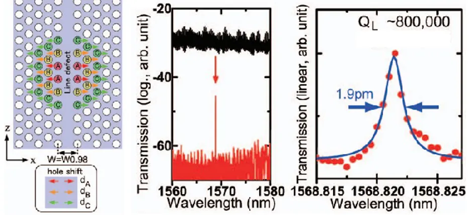
The last scheme of PhC cavity that we want to briefly describe is the one that exhibits up to now the highest Q factors in SOI: this kind of cavities were obtained by properly produce a local modulation of a line defect. This intriguing design was proposed by Notomi group [21, 23] and it is also based, similarly to the previous case, on a line defect, a waveguide, in a PhC slab.
Figure 2.10: Schematic of PhC cavities realized by a waveguide width modulation (left) and transmission measurements (center, right) showing a ultra-high Q factor, as high as 80000. Adapted from [23].
In this case a waveguide is locally modified by performing a shift of some holes, in order to make a local confinement potential. Such a shift can be done with the aim of creating a sort of elliptic distribution of holes, as depicted in the schematic of fig. 2.10 (left panel). The waveguide width at the center of the cavity is increased by displacing the holes called A, B, C, by dA > dB ≥ dC.
The Q factor was measured by using a tunable laser diode coupled to an input waveguide with a fiber, and a photodetector coupled to an output waveguide. The transmission in such a structure reveals that the linewidth is as narrow as 1.9 pm, corresponding to a loaded Q value of about 800000, at about 1.5 m (see fig. 2.10, center and right panel).
A key point of these structure is also that it is possible to have very high Q factors even with very thin barriers on the top/bottom sides of the cavity. Some air slots delimitating the PhC at 4 rows of holes already determine an experimental Q even larger than 106 [21].
This latter result was obtained by realizing the device depicted in fig. 2.11, where q is the number of the rows, i.e. 4 in this case, a = 420 nm, and ma is the total length of the air slot. By using this particular design a linewidth of just 1.2 pm was measured.
Figure 2.11: SEM picture of a nanocavity with q = 4 and m = 24 and measurement of the fundamental cavity resonance, showing a linewidth of 1.2 pm (a Q exceeding 106).
Therefore we can see how effective is a proper design in order to achieve Q factors really comparable with those of the microring resonators, but with a much smaller size and much smaller Q/V values.
Chapter 2 – Photonic Crystals 2.3.5 Efficient light extraction out of a PhC cavity
The Q factor is a very important feature of the PhC cavities. The ultimate designs showed before demonstrate that it is possible to realize in practice ultra-high Q cavities with unprecedented (diffraction limited) volumes. It is worth reminding that the Q factor represents the number of travels forward and backward that photons can do in the cavity before coming out as losses. A high Q factor is fundamental, because it pushes up the Purcell effect. On the other hand, for practical applications on photonic chips, the off-plane radiation could be useful, in order to control both the in- and the out-coupling of light. This is important in emission experiments, such as photoluminescence from active media within the PhC pattern [29], or for optically pumping nanophotonic devices.
Figure 2.12: (a) Schematic of far-field optimized L3 PhC cavity. Red holes are shifted and shrunk for the gentle confinement effect. Brown holes increase the out-of-plane coupling. (b) Calculated Q factor and out-coupling efficiency. The parameters are: thickness of the slab th = 220 nm, lattice constant a = 420 nm, holes’ radius r = 0.265 a, red holes shift x = 0.16 a, red holes shrinking r’ = -0.06 a. Adapted from [30].
We have seen that by performing local adjustment of the geometric distribution of the holes the Q factor is clearly optimized, thanks to the reduction of the coupling to the radiative modes. The same idea can be exploited for another important purpose, that is to keep a relatively high Q
factor, increasing at the same time the out-of-plane radiation in a controlled way. A systematic study regarding this issue is reported in ref. [30].
The physics behind the out-of-plane coupling is like that of a grating effect: the Fourier components of the field lying beyond the light cone, can be folded back around |k|=0 (i.e. close to the normal direction with respect to the cavity) by superimposing a lattice with twice the periodicity of the basic PhC structure [31]. This trick allows to have a good light extraction from the surface.
The idea of finding a trade-off between the Q factor and the out-of-plane coupling is depicted in fig. 2.12 for L3 cavities. In fact the cavity is
Q-optimized, by applying the gentle confinement effect: in the schematic of panel (a) the edge holes, highlighted in red, are shifted and shrunk, making gentler the cavity boundaries. In the same picture, note that the dark holes are distributed with a longitudinal lattice parameter that is actually 2a, thus forming the grating. This second lattice is characterized by a different holes radius, and in panel (b) the trends of the calculated Q factor and out-coupling efficiency are plotted as a function of the enlargement r’’ of these new holes (highlighted in brown in the picture) with respect to the original ones.
Figure 2.13: (a) Resonant scattering measurement from L3, L5 and L7 cavities, as a function of the enlargement. (b) Corresponding figure of merit, given by the product of the Q factor and of the resonant scattering efficiency [30].
Chapter 2 – Photonic Crystals
Ln cavities were realized as air-bridges in SOI and the experimental
results (see fig. 2.13 (a)), obtained by resonant scattering measurements [32] are comparable with the theory [30]. Additionally, a figure of merit given by the product Q times the efficiency is suggested (see fig. 2.13 (b)). The maximum value of this product, as a function of the holes enlargement represents the solution to the trade off between confinement (the Q) and extraction (the out-coupling efficiency), and it is at about r’’ = +6 nm, with Q factors as high as 62000 [30]. This interesting study therefore indicates that it is possible to efficiently engineer the holes distribution in a PhC cavity, achieving a very high Q factor and at the same time a strong out-of-plane coupling efficiency.
2.4 PhC-based nanodevices
In this last section some of the most interesting advantages of PhC and their applications will be shown. Actual devices like lasers were successfully demonstrated recently. Additionally, due to the strong confinement, other interesting effects were observed in PhC waveguides, like slow light. This particular regime, that will be discussed below, allows a strong light-matter interaction, thus increasing the probability of non-linear effects [33].
2.4.1 Slow light
The light speed c is very advantageous in photonics, being the main motivation for the research in optoelectronics. The data transmission between two points can be done with photons at their extremely high speed, and this is true whatever is the distance, either on a global scale, or in the same photonic chip. Despite these undoubted advantages, however, due to the ultra-high value, it is very difficult to control light in the time domain. This is a problematic issue if we think at key devices like optical buffers, acting in the all-optical photonic chips of the next generation information networks. This problem occurs also in multiplexing, retiming and in performing convolution integrals. Engineered photonic crystals allow to overcome this difficulty, because they can actually control the speed of light [33-36] and enhance the effect of some weak interactions.
Slow light stands for light with a low group velocity, i.e. a low speed at which an optical pulse envelope propagates. The group velocity is given by:
(2.14)
where (k) is the dispersion relation, linking the frequency to the wavevector k. The group index ng is defined as c/vg, while on the other hand
the phase velocity v is the ratio c/n.
The nature of the delay in photonic crystals can be easily described with the picture reported in fig. 2.14. With respect to a normal waveguide, the main advantage of PhC is that light is coherently backscattered at each single unit of the crystal (fig. 2.14 left). The PhC acts like a unidimensional grating. If the forward and the backward waves agree in phase (and they do at the edge of the Brillouin zone, where k = /a) a standing wave is formed, which is a wave with a zero group velocity.
If we slightly move away from the edge, we enter in the slow light regime, because the forward and the backward waves are “almost” in phase and the interaction is a slowly moving interference pattern. The field goes 2a back and moves 3a forward, for instance. This is a slowed down pattern. This is slow light. This phenomenon does not occur anymore when we move further away from k = /a, because the two waves cannot interact and the waveguide behaves normally.
Figure 2.14: Two mechanisms for obtaining slow light in a PhC waveguide: coherent backscattering (left) and omnidirectional reflection (right) [34].
Another possible mechanism is due to the omnidirectional reflection that occurs in a PhC. This means that whatever is the propagation angle
d
,
d
gv
k
Chapter 2 – Photonic Crystals
(even close to the point, k ≈ 0) light is reflected. This particular case is depicted in the right panel of fig. 2.14 and shows that these modes have a very small forward component in k, thus travelling in a slow light regime.
The slowdown factor S can be defined as the ratio of the phase velocity over the group velocity S = v /vg. A group index ng = 100
corresponds to a slowdown factor of about 50, if the refractive index of the material is 2 (these are typical numbers). Recently this performance was achieved for SOI slabs [37].
Figure 2.15: Dispersion relation (k) showing the fast light regime and the slow light one [35].
One of the most interesting effects of slow light regards the optical switching of a light signal. Optical switching exploits a phase change, typically expressed by kL: in the Mach-Zender interferometer, for
instance, for kL = there is a complete switch on/off [33]. A change of the refractive index is able to modify the dispersion relation, as depicted in fig. 2.15. When the refractive index is tuned, the dispersion relation is shifted upwards (dashed line). In the fast light regime (steep gradient), at the frequency 1, the change in k is small. On the other side, in the slow light
regime (shallow gradient), at the frequency 2, the change in k is large,
thus enhancing the optical switching operation.
A demonstration of this important effect is reported in ref. [38], in which a 5 m-long optical switch was realized with a change in refractive index n = 4×10⁻³. The typical length of a conventional waveguide would be
Another promising application of slow light regards non linear optics. In fact, when an optical pulse travels in a slow light waveguide, it is squeezed in a smaller space, thus increasing its energy density. Therefore in this way, the light-matter interaction can be very high. A very interesting result recently obtained is the third harmonic generation in SOI PhC slab waveguides [40]. This is a non linear effect that means the generation of a light (with intensity I3 and frequency 3 ) starting from a fundamental beam
(I and It depends on the third-order non linear susceptibility (3) and on the cubic power of I , being actually a transformation of three photons into a single 3 photon (see fig. 2.16(a)).
Figure 2.16: (a) Schematic of the slow light PhC waveguide with the third harmonic generation. (b) SEM image of the waveguide feeding the PhC waveguide etched in a thin Si membrane [40].
I is proportional to the pump power and to the group index and it is
inversely proportional to the effective area of the fundamental mode. Therefore by using both the light confinement provided by the PhC and the enhanced energy density due to the slow light effect, it is possible to generate third harmonic light. The pump power required for observing light emission at 520 nm in Silicon can be thus reduced to just 10 W [40]. Additionally the PhC around the line defect can be engineered in order to act as a grating, thus helping in the extraction of this light, that on the contrary would be strongly absorbed by the material.
![Figure 2.3: Band structure of an array of alumina columns surrounded by air in a square lattice distribution (top panel) and of a triangular lattice with holes of air in a dielectric (bottom panel) [10]](https://thumb-eu.123doks.com/thumbv2/123dokorg/4482929.32394/24.892.297.605.481.905/figure-structure-surrounded-lattice-distribution-triangular-lattice-dielectric.webp)