UNIVERSITÀ DEGLI STUDI DI CATANIA
Dottorato di Ricerca in Scienza e Tecnologia dei Materiali - XXVIII cicloVincenzina Strano
Low-cost ZnO nanostructures:
controlled synthesis and applications
Tutor: Prof.ssa M. G. Grimaldi
Supervisor: Dr. S. Mirabella
Coordinatore: Prof.ssa M.G. Grimaldi
UNIVERSITÀ DEGLI STUDI DI CATANIA
Dottorato di Ricerca in Scienza e Tecnologia dei Materiali - XXVIII ciclo
Vincenzina Strano
Low-cost ZnO nanostructures:
controlled synthesis and applications
Tutor: Prof.ssa M. G. Grimaldi Supervisor: Dr. S. Mirabella Coordinatore: Prof.ssa M.G. Grimaldi
Cover
False colored SEM image in cross view of ZnO NWL/NR, a novel combined nanostructures obtained by chemical bath deposition with ZnO NWLs grown on top of ZnO NRs. More details can be found within the Summary of this thesis.
Low-cost ZnO nanostructures: controlled synthesis and applications Vincenzina Strano
Ph.D. Thesis, University of Catania Printed in Catania, December 2015
All have their worth and each contributes to the worth of the others.
from The Silmarillion
J. R. R. Tolkien
Contents
Introduction ... 1
Chapter 1 ZnO: Properties, Synthesis and Applications ... 5
1.1 Fundamentals of ZnO ... 6
1.1.1 Crystallographic Properties of ZnO ... 8
1.1.2 Band Structure and Optical Properties ... 11
1.1.3 Electric and Piezoelectric Properties... 14
1.2 Applications of ZnO Nanostructures ... 17
1.2.1 Energy Harvesting Devices ... 17
1.2.2 UV Detection and Lighting ... 21
1.2.3 Sensing ... 23
1.3 Synthesis of ZnO nanostructures ... 25
1.3.1 Vapor Phase Synthesis Methods ... 25
1.3.2 Solution Phase Syntheses Methods ... 26
1.4 ZnO Nanorods: Key Features in CBD ... 30
1.5 ZnO Nanowalls: a brand new material ... 38
Chapter 2 ZnO Nanorods Growth by Chemical Bath Deposition ... 43
2.1 HMTA, the key player ... 44
2.2 ZnO NRs Synthesis and Structural Characterizations ... 48
2.2.1 Seed Layer Preparation ... 49
2.2.3 Structural Properties... 54
2.3 Growth Kinetics ... 57
2.4 Role of HMTA ... 62
2.5 Steric Hindrance Effect ... 67
2.6 Conclusions ... 72
Chapter 3 Light Scattering with ZnO Nanorods ... 75
3.1 Nanostructures for cost effective Photovoltaics... 76
3.1.1 Light Trapping Approaches ... 76
3.1.2 Light ScatteringPerformance of solution derived ZnO NRs . 81 3.1.3 Decoupling the light diffuser layer: a new way ... 83
3.2 ZnO Nanorods on Transparent Substrate ... 84
3.2.1 Morphological and Structural Properties ... 84
3.2.2 Optical Analysis ... 87
3.3 Effect of ZnO NRs light diffuser layer on c-Si Solar Cell ... 92
3.4 Conclusions ... 96
Chapter 4 ZnO Nanowalls by CBD: Growth and Applications ... 97
4.1 ZnO Nanowalls growth: role of pH ... 98
4.2 Pre-anodization of Al substrate ... 104
4.3 Growth Kinetics and Model ... 109
4.4 ZnO Nanowalls as pH sensitive material ... 114
4.5 Photocatalytic Performance of ZnO NWLs Films ... 118
4.6 Conclusions ... 123
Summary and Perspectives ... 125
Curriculum Vitae ... 147 Acknowledgments ... 149
Introduction
Advances in nanotechnology is strongly dependent on research innovative nanostructured materials in nanostructure form. Multifunctional metal oxides have recently emerged as smart materials with a wide range of controllable properties leading to innovative device concepts. In particular, zinc oxide (ZnO) presents an unique combination of interesting properties such as non-toxicity, wide band-gap, high exciton binding energy at room temperature, piezoelectric behavior, high physical, chemical and mechanical stabilities [1]. Research on ZnO is an old story. In 1957, the New Jersey Zinc Company published a book entitled “Zinc Oxide Rediscovered” to promote the material’s properties worthy to be further investigated [2]. Since then, ZnO have gained growing importance in the material science. In the last decade, ZnO nanostructures have been the focus of intensive studies, being an almost ideal systems both from a fundamental point of view (ease of nanostructuration, energy band bending, intrinsic and extrinsic defects, combination of polar and non-polar planes, …) and from the applications (energy harvesting devices, sensors, biomedical devices, lighting, …). Many methods, both physical and chemical, have been employed for the synthesis of nanostructured ZnO; however most of the synthesis methods involve expensive experimental set up and sophisticated equipment. One of the basic requirements for nanomaterials to become industrially viable is the low production cost alongside the possibility to supply large amount of non-toxic material. In this regard, wet-chemical synthesis approaches are very appealing, having the advantages of easy use, low cost, reduced process temperatures and potential for scaling up. On the other hand, these kinds of synthesis have the shortcoming of lack of a good control and reproducibly. Overcoming these limitations and ensuring a high degree of reliability represent important challenges for modern material science. Among the wet-chemical approaches, wet-chemical bath deposition (CBD) has emerged as the
simplest and more versatile method for the synthesis of ZnO nanostructures. It is a chemical process, similar to an electroless deposition of solid phase from an aqueous solution. In this thesis, the attention is reserved to ZnO nanorods (NRs) and nanowalls (NWLs). ZnO NRs grown by CBD are among the most promising semiconducting nanostructures currently investigated for a wide range of applications. ZnO NWLs represent a new form of nanostructure with very large surface area, easy to synthesize by CBD on Al-covered substrate. Currently, some investigations have been focused on the microscopic mechanisms leading to the formation of ZnO NRs and NWLs, however some outstanding issues remain to be solved. A clearer comprehension of the growth mechanism in CBD and a better control of the synthesis are fundamental issues for taking full advantage of this technique. The work described in this thesis aims to deeper understand the mechanisms underlying the formation of ZnO NRs and NWLs under CBD conditions, attempting to clarify the role of synthetic parameters. Discerning their effects leads to enhance the control over the growth process. The potentialities of ZnO NRs and NWLs with optimized morphologies as critical components in technological solar cell, photocatalysis and sensing applications are also investigated.
The thesis is organized as follows:
The first chapter is devoted to a review of the basic physical properties of ZnO and its nanostructuration. A brief selection of the different promising applications of ZnO nanostructures is reported followed by detailed description of some chemical and physical approaches for the synthesis of ZnO nanostructures. In particular, a survey of the literature about the low-cost chemical bath deposition of ZnO nanorods and nanowalls is presented.
In the second chapter, a systematic investigation of the chemical bath deposition of ZnO NRs using an aqueous solution with zinc nitrate salt and hexamethylenetetramine (HMTA) is presented. An optimized procedure for reproducible synthesis and the growth kinetics are presented and discussed. In addition, an empirical study is reported evidencing the double
role of HMTA in the NRs growth mechanism. HMTA is shown to participate both as a supplier of OH− ions and as a capping agent promoting
the anisotropic growth. These two actions are not mutually exclusive, and the amount of HMTA in solution determines the key process variable. This result contributes as a step towards a better control of CBD synthesis.
In the third chapter the light scattering effects from ZnO NRs grown by CBD on flat and transparent substrate are examined, giving particular emphasis to forward light scattering efficiencies. ZnO NRs with different morphological features showed an high efficiency in forward diffusion of visible light. By analyzing and modeling the light scattering performances, a threshold in NRs length (1µ) was identified over which the light scattering effect is enhanced. The applicability of ZnO NRs film as low-cost light diffuser layer upon crystalline silicon (c-Si) solar cell is also presented. An enhancement of the light-current conversion efficiency has been achieved for wavelengths longer than 600 nm, attributable to the scattering of light by NRs array.
The fourth chapter presents the main results about the synthesis and application of ZnO NWLs. In particular, the effects of the solution composition, pH, concentration of Al(OH)4−and growth time on the quality
of ZnO NWL films grown by CBD are examined. A prior oxidation of Al substrate is proposed as a new, easy and inexpensive route for enhancing the quality of ZnO NWLs. A self-screening model has been developed to explain the growth kinetics of ZnO NWLs. The promising results of ZnO NWLs as pH sensing material and as photocatalyst substrate are finally shown.
Chapter 1
ZnO: Properties, Synthesis and Applications
Low-dimensional ZnO structures have recently attracted more and
more interest in scientific research. In the last years, ZnO nanowires
and nanorods have been defined as the most representative
one-dimensional nanostructures, together with silicon nanowires and
carbon nanotubes. Indeed, the number of publications and the
cross-referenced areas based on ZnO nanostructures are as large and
important as literature in quantum computing, carbon nanotube,
semiconductor thin films, and dark matter [3]. The reasons of this
great interest can be also ascribed to the ease of growing
nanostructures with noticeable performances and in a large number
of intriguing shapes.
In this chapter the basic physical properties of ZnO are described.
Then, a brief selection of the different promising applications of ZnO
nanostructures is reported followed by detailed description of some
chemical and physical approaches for the synthesis of ZnO
nanostructures, with particular attention to low-cost chemical
deposition of ZnO nanorods and nanowalls.
1.1 Fundamentals of ZnO
Zinc oxide (ZnO) is a II-VI inorganic semiconductor, relatively abundant in nature as mineral zincite and it is widely used in various industrial products as summarized in Figure 1.1 [1].
ZnO has been investigated as semiconductor material since the 1930s [4]. Between the beginning of the eighties and mid-nineties, the research on ZnO suffered a setback, partially due to the difficulty to achieve a robust p-type doping. Furthermore, at that time, the interest was directed to III-V semiconductors whose ambipolar doping and nanostructuring were already easy to obtain [5]. Conversely, in the last 20 years, ZnO has experienced a renewed interest in scientific research pushed by its great versatility in terms of synthesis methods for epitaxial layers and nanostructures and for related potential applications.
Figure 1.1: Industrial applications of ZnO. Scheme adapted from ref [1].
The new era for ZnO started in the field of optoelectronics, fueled by the impressive progress in developing efficient short wavelength emitters based on wide band-gap semiconductors. GaN based structures were the focus of
Applica
tion
of
Z
nO
Pharmaceutical andCosmetic Industires powders, dental paste, etc. Component of creams,
Rubber Industry Fillers, activator of rubber compounds
Textile Industry Absorber UV radiation
Photocatalysis Photocatalyst
Electro/Nanotechnology Emitters, Sensors, Solar Photoelectronics, Field Cells, etc. Other Applications Biosensors, Prodiction of zinc silicates, etc.
many work since GaN p-n junctions showed favorable performance as blue/UV diodes and lasers [6]. The need to find high quality, closely lattice matched substrate for GaN, stimulated the research on ZnO that provides a close match in addition to the possibility to grow large bulk single crystal [7]. Thereafter, not only the versatility of ZnO was revaluated but also new potentialities were defined [5, 8, 9].
Figure 1.2: A collection of ZnO nanostructures: (a) nanobelt; (b) aligned nanowire
arrays; (c) nanotubes; (d) array of propellers; (e) mesoporous nanowires; (f) cages and shell structures; and (g) hierarchical shell and propeller structure. The percentage in each figure indicates the purity of the as-synthesized sample for the specific nanostructure. Adapted from ref [10].
(a)
(b)
(c)
(d)
(e)
One of the most intriguing aspect of ZnO is the possibility to easily grow many different nanoscale forms. Figure 1.2 (a-g) reports a collection of ZnO nanostructures: nanobelt (NBs), aligned nanowires (NWs) and nanorods (NRs), nanotubes (NTs), nanopropellers, porous NRs and hierarchical nanostructures. Current research has been focused on these nano and micro scale structures, representing the fundamental building blocks of the modern physical science and engineering. The reduction in size provides the opportunity of developing new generation devices compared to conventional bulk materials. Table 1.1 lists several physical properties of wurtzite ZnO, most of which are pertinent also to low dimensional material, though it is know that the nanostructuring leads to effects - quantum confinement effect and enhanced surface states- affecting some important properties such as quantum transport and enhanced radiative recombination of carriers [11-14].
Properties Value
Lattice Constant (300 K) a=3.250 Å; c=5.207 Å
Density 5.606 g/cm3
Melting Point 2248 K
Refractive index 2.008, 2.029
Band Gap Energy 3.44 eV - 3.37 eV
Exciton Binding Energy 60 meV
Effective Mass 0.24 (electron); 0.59 (hole)
Mobility 100-200 cm2/Vs (electron); 5-50 cm2/Vs (hole)
Table1.1: Physical and structural properties of wurtzite ZnO.
1.1.1 Crystallographic Properties of ZnO
Under ambient conditions, the crystal structure of ZnO is preferentially the hexagonal wurtzite with lattice parameters a=3.250 Å and c=5.207 Å [15] in which each Zn anion is surrounded by four O ions at the corners of a tetrahedron, and vice versa (Figure 1.3(a)).
Figure 1.3: (a) Wurtzite Structure of ZnO. O atoms are shown as red spheres, Zn
atoms as grey spheres. The unit cell is identified by black lines. (b) The projected structure of ZnO along a-axis, showing the {0001} and {0111} polar surfaces. Adapted from [10].
It is worth noting that for hexagonal crystals, four-indices (hkil) system, is used to indicate the crystallographic planes and direction, instead of usual three-indices (hkl) Miller notation. The index i is given by the h+k+i=0. This four-axis representation is called Miller-Bravais and it takes into account the crystal symmetry of hexagonal structure, avoiding that crystallographic equivalent planes are indicated with dissimilar indices. The tetrahedral coordination is typical of sp3 covalent bonding nature, however ZnO, as the other II-VI compounds, has a strong ionic characteristic as demonstrated by its ionicity fi=0.616, border value between covalent and ionic semiconductor [12]. This fraction of ionic binding is responsible for the large gap between the conduction and valence bands (ZnO energy bandgap Eg=3.44 eV, at low temperature) [5].
ZnO can also crystallize in cubic zinc blende, a metastable phase that can be made stable only by heteroepitaxial growth on cubic substrates,
and in rocksalt structure, high-pressure metastable phase [16]. All the crystalline forms of ZnO exhibits crystallographic polarity which contributes to many properties of ZnO, as piezoelectricity, and affects the growth mechanisms and the defect generation. In wurtzite ZnO structure, along the <0001> direction (c-axis), there is an alternation of Zn-terminated (0001) and O-terminated (0001) polar planes. The {1011} planes of wurtzite ZnO are another group of polar planes with higher surface energy (see Figure 1.3(b)). Other common crystal faces terminations are the non-polar (1120) and (1010), both containing the same number of Zn and O atoms. Figure 1.4(a-c) reports some typical growth morphologies of ZnO one-dimensional (1D) nanostructures in which the non-polar planes (0110) and (2110) results maximized because of their lower surface energies. On the other hand, introducing planar defects parallel to the polar faces allows to grow structures dominated by polar surfaces, as in the case of nanobelt shown in Figure 1.4(d).
Figure 1.4: Typical growth morphologies of one-dimensional ZnO nanostructures
1.1.2 Band Structure and Optical Properties
A precise knowledge of the band structure is crucial for understanding the potential applications of a semiconductor. Consequently, many studies, both theoretical and experimental ones, were devoted to calculate the band structure of ZnO [17-22]. The bottom of the conduction band (CB) is formed by the 4s levels of Zn2+ and the top of the valence band (VB) by O2- 2p and Zn2+ 3d states. The early attempts to theoretically
determine the electronic band structure ruled out the effects of Zn 3d states, considering them as core level, and the results were not in good agreement whit the experimental data. In 1995 a novel approach was proposed, consisting in incorporating an atomic self-interaction correction into usual local density approximation (LDA) [20]. The calculations, reported in Figure 1.5, showed that the maximum of VB and the minimum of CB energy values were obtained at Γ point k =0, which confirmed that ZnO is a direct band gap semiconductor.
Figure 1.5: LDA bulk band structure of ZnO as calculated by using the
self-interaction correction.The horizontal dashed lines indicate the measured gap energy and d-band width [20].
Moreover, the calculated value of the energy gap was 3.77 eV and it is the closest to the experimental one (Eg=3.37 eV at room temperature, [23]) until
then. As mentioned above, such wide and direct bandgap of ZnO enables promising application in blue/UV range photonics as well as the large exciton binding energy (60 meV) [7, 24] indicates an efficient excitonic emission even at room temperature (RT).
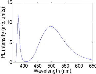
Typical room-temperature (RT) photoluminescence (PL) spectrum of ZnO consists of a UV emission band and, eventually, a broad visible emission band, as shown in Figure 1.6. Most of works suggested that the UV emission at RT originates from the radiative recombination of excitons [25-27], while some authors proposed that such emission can also contains the contributions related to unspecified localized state [28] and to the free-to-bound transitions [29].
Figure 1.6: A typical room temperature PL spectrum of ZnO nanowires grown on a
Si substrate using the vapor liquid solid technique at 890 °C [30].
The broader emission observed in the visible region of the spectrum is generally ascribed to impurities and different intrinsic defects, such as oxygen vacancies (Vo), zinc vacancies (VZn), zinc interstitials (Zni) and
oxygen interstitials (Oi). This visible band emission is, in particular, a typical
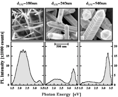
optical feature of ZnO nanostructures. Shalish et al., analyzing the PL spectra of ZnO NWs grown by high temperature (1000°C) chemical vapor deposition (CVD), demonstrated that this deep-level luminescence is mainly due to electronic states close to the surface. As a consequence, the reduction of the nanostructures size leads to an increase of the relative intensity of this emission. Figure 1.7 reports the PL spectra and scanning electron microscopy (SEM) images of the ZnO NWs with different diameters. The ratio between the UV and visible luminescence peak intensities changes with the size of the nanowires.
Figure 1.7: Photoluminescence spectra and related SEM images obtained from ZnO
NWs grown by CVD with different diameter (dNW). Adapted from [31].
However, the exact identity of the defects responsible for the visible emission band is still unclear and widely debated. Moreover, some variation
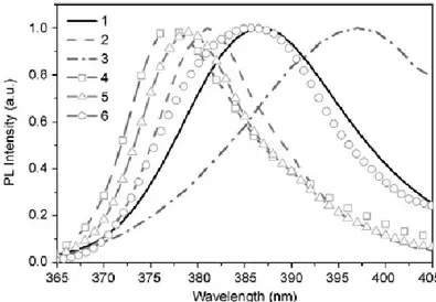
of the position of the UV peak was observed for different shaped nanostructures, as illustrated in Figure 1.8 [32]. One possible explanation for this variation may be the difference in surface-to-volume ratio entailing different defects concentration (defect density on the surface is higher than in the bulk [33]).
Figure 1.8: RT PL spectra in the UV range for different nanostructures: (1)
Tetrapods, (2) Needles, (3) Nanorods, (4) Shells, (5) Highly faceted NRs, (6) Ribbons. Adapted from [32].
1.1.3 Electric and Piezoelectric Properties
As-grown ZnO shows n-type conductivity. For long time, the causes for this unintentional n-type doping were attributed to the presence of native defects as Vo or Zni [34,35]. However, more recent works have claimed that
neither oxygen vacancies nor other point defects can contribute to n-type conductivity [8, 36]. In particular, several theoretical calculations, corroborated by experimental evidences, have shown that Vo is a deep level
defect state (DLS) [37,38] and thus it cannot significantly contribute to n-type conductivity. Moreover, Kohan et al. [39] showed that theoretically both Vo and Zni have high formation energies in n-type ZnO. Further studies
proved that the inclusion of substitutional H (much more stable than interstitial H), acting as a shallow donor, is main responsible of the
unintentional n-type doping. [40,41].
The electrical properties of ZnO, in terms of carrier concentration and mobility, are closely correlated to the method used to synthesize the material. The room-temperature electron mobility for bulk and thin film ZnO are in the range of 100-200 cm2/Vs [42, 43], typically measured by Hall effect analysis. These values are close to the theoretical value of 300 cm2/Vs estimated by Monte Carlo simulations for the room temperature
electron mobility of ZnO [44]. Electrical transport measurements were also performed on individual ZnO nanowires and nanorods [45]. Park et al. [46] reported on fabrication and electrical characteristics of high-mobility field-effect transistors (FETs) using a single ZnO nanorod, Figure 1.9, measuring an electron mobility of 75 cm2/Vs.
Figure 1.9: (a) Schematic and (b) SEM image of ZnO NR FET device [46].
The effect of surface states on the electron transport was eliminated by coating with polyimide known for the effective passivation effect in bipolar technology. After polyimide deposition, the field effect mobility of ZnO NR
FET was highly increased to 120-3100 cm2/Vs with mean value of 680
cm2/Vs [46]. These results indicate that the ZnO nanostructure based devices
can have higher performance than their thin film counterpart. Although as-grown ZnO is n-type material, intentional n-type doping is required to increase the carrier concentration in view of electronic device applications. Al, Ga and In are the most common donor dopants for ZnO, giving rise to transparent conductive oxides (TCO) commonly employed in a large number of devices [47]. One of the major hindrance for fully exploiting ZnO in electronic and photonics technology is the difficulty of achieving a stable and reproducible p-type doping [8, 16]. Beyond the tendency toward n-type conductivity, the compensating effect from intrinsic defects and the small number of candidate for shallow acceptor represent severe limitations for p-doping of ZnO [8].
ZnO exhibit also a large electromechanical response caused by the lack of a center of symmetry in the unit cell. By exerting an external pressure, a lattice distortion is induced and the center of the negative charges will no longer coincide with the center of the positive charge, generating an electric dipole. The mechanism is outlined in Figure 1.10.
Figure 1.10: Schematics showing piezoelectric effect in tetrahedrally coordinated
cation-anion unit [10].
An important parameter evaluating piezoelectric performance is the d33
piezoelectric coefficient. For ZnO the d33 value is about 9.9 pC/N for a bulk
and 12.4 pC/N for an oriented film [48, 49] but these value can be improved by doping with transition metals atoms [50, 51]. Therefore, ZnO, especially
in nanostructural formats, has been used for building micromechanical devices, such as sensor, actuators and nanogenerators.
1.2
Applications of ZnO Nanostructures
The present renaissance of the scientific interest for ZnO is based on the wide range of promising applications in a large number of emerging areas. Several examples of energy harvesting and sensing devices based on ZnO nanostructures are briefly reported below.
1.2.1 Energy Harvesting Devices
The semiconducting and piezoelectric dual properties of ZnO may be exploited for applications in mechanical-energy conversion or in electrical power generation by solar cells. A shining example of electromechanical application of ZnO nanostructures is in piezoelectric nanogenerator [52]. By using zinc oxide nanowires arrays it has been possible to convert nanoscale mechanical energy into electrical energy (Figure 1.11). The aligned NWs are deflected with a conductive atomic force microscope tip in contact mode. The bending creates a strain field which causes, for piezoelectric effect, an electric field across the nanowires. This effect can be used in different application as in the case of wireless devices devoted to in situ, real-time biomedical monitoring and detection. Such devices should be self-powered and not dependent on a battery. Compared to conventional transducers based on piezoelectric thin films, the nanostructures not only might improve the general device performances (critical strain, flexibility, sensibility, operative lifetime) but also reduce the size of integrated nanosystem.
Figure 1.11: (a) SEM images of ZnO NWs, (b) Experimental setup for generating
electricity by deforming a piezoelectric ZnO NW with a conductive AFM tip. The base of the NW is grounded and an external load RL is applied, which is much larger than the resistance of the NW. Adapted from [52]
Zhu et al. [53] reported a flexible high output nanogenerator (HONG), based on a lateral ZnO nanowire (Figure 1.12). The generated electric energy was successfully used to power a commercial light-emitting diode (LED).
Figure 1.12: (a) Schematic of HONG’s structure without mechanical deformation.
Gold is used to form Schottky contacts with the ZnO NW arrays. (b) Output scaling-up when mechanical deformation is induced, where the “” signs indicate the polarity of the local piezoelectric potential created in the NWs. Adapted from [53].
ZnO nanostructures are also suitable for photovoltaic application. The low reflectivity helps to optimize the light absorption, the high surface-to-volume ratio increases the charge separation probability and the effective electron transport along 1D structures enhances the charge collection. The potentialities ZnO nanostructures have been investigated in herojunction device as demonstrated by several papers published on n-ZnO/p-CuO2 solar
cells [54]. Moreover, considerable interest is focused on ZnO-based dye-sensitized solar cells (DSSCs) [55, 56], organic solar cells (OSCs) [57, 58], and hybrid organic-inorganic solar cells (HSCs) [59, 60]. These kinds of device represent promising approaches for inexpensive, large-scale solar energy conversion. In 2005, M. Law et al. first introduced a new version of the dye-sensitized cell in which the traditional nanoparticle film was replaced by a dense array of oriented ZnO nanowires [56], reaching a conversion efficiency =1.2-1.5% (Figure 1.13).
Figure 1.13: (a)Schematic diagram of ZnO NWs based dye sensitized cell. (b) SEM
cross-section of ZnO NWs array on FTO. Scale bar, 5 µm. Adapted from [56].
In HSCs, ZnO nanostructures are widely used to replace the electron acceptor organic semiconductors used in pure organic solar cells. Inorganic semiconductors, ZnO in particular, have higher electron mobility and chemical stability compared to those of organic semiconductor. Moreover, the versatility of ZnO nanostructures has led to the application of ZnO in solar cells with different device architectures, as shown in Figure 1.14. The power conversion efficiencies are typically below 1%, much lower than
those related to fully OSCs. Mainly, this may be due to the limited polymer infiltration in ZnO nanostructure as well as low polymer/ZnO wettability. [59, 61].
Figure 1.14: Schematic diagrams of ZnO nanostructures/organic semiconductor
HSCs. (A) ZnO- nanocrystals (NC)/organic bulk heterojunction HSCs with randomly dispersed ZnO nanocrystals; (B) ZnO-NR/organic HSCs with vertically aligned ZnO nanorods. Adapted from [61].
Compared to ZnO/organic HSCs, the application of ZnO nanostructures as cathode buffer layer (CBL) or transparent electrode in OSCs are more promising [57, 62, 63]. ZnO films and nanostructures, by creating an Ohmic contact with the acceptor material, collect and extract electron carriers while block hole carriers. The improved carrier collection across the interface enhances the efficiency of the device.
1.2.2 UV Detection and Lighting
UV detection is another promising application of ZnO nanostructures. Photodetectors sensitive to UV radiation have a huge potential in spectroscopy, sensing device, astronomical studies and optical communications [64]. These technologies require the detection of UV light without the influence of visible or infrared light, in order to minimize the background signal and avoid erroneous detection. ZnO nanorods and nanowires, changing their electrical potential under UV irradiation, are particularly suitable for this purpose due to higher spatial resolution compared to thin film. The first individual ZnO-based nanowire photodetectors were reported by Kind et al. in 2002 [65]. The conductivity of the ZnO nanowires was extremely sensitive to UV light exposure (365 nm) and increases by a typically four to six orders of magnitude as shown in Figure 1.15.
Figure 1.15: Reversible switching of a ZnO nanowire between low and high
conductivity states when the UV-lamp (365 nm) was turned on and off. The bias on the nanowire is 1 V [65].
Many efforts were devoted to properly describe the mechanisms driving the UV sensing [8, 66]. It is generally supposed that atmospheric oxygen O2 was
absorbed at the Vo sites on ZnO surface. Under UV illumination, electron-hole pairs are generated, electron-holes migrate to the surface where O2 desorption
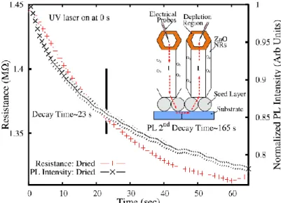
occurs. At the same time, the unpaired electrons contribute to enhance the conductivity. Recently, ZnO NRs grown by chemical bath deposition (CBD) within this PhD thesis work aimed to understand the role of the defect states with respect to O2 desorption [67]. ZnO NRs exhibited two main PL peaks
related to surface defects at 555 nm - originated from single ionized oxygen vacancy (Vo+) - and 610 nm - due to Vo. In particular, the 555 nm PL
intensity showed a transient in air 20 s, which was correlated with the change in resistance under UV excitation, as shown in Figure 1.16. This correlation arises because O2 desorption decreases the band bending and thus
the concentration of Vo+ states; simultaneously, charge separation reduces
the sample resistance. On the other hand, the PL transient was suppressed in vacuum, because the depletion region is stable since O2 desorption does not
occur.
Figure 1.16: Comparison of the resistance and 555nm PL transient for ZnO NRs
grown by CDB and dried in air at 100°C . Both transients have a decay time of 23 s. The inset represents the resistance measurement geometry. Adapted from [67].
ZnO nanostructures are attractive also for light emitting diodes (LED) and lasing in blue-UV spectral region. In 2001, room temperature UV
lasing in ZnO-nanowires was demonstrated [68]. Homojunction LEDs based on p-ZnO/n-ZnO structures are generally difficult to achieve due to the unavailability of high quality and stable p-type doping of ZnO. However, heterojunction LED using the combination of n-type ZnO with various p-type materials have been investigated [69].
1.2.3 Sensing
ZnO is widely employed also in chemical, gas and bio-sensing because it is particularly sensitive to the chemical environment. In particular, the nanostructures have the great advantages of high surface area over planar device configuration. The detection of gas is usually achieved using a conductometric gas sensor, since the adsorption of the gas on the sensor surface causes a change in its conductivity [70]. Hydrothermally grown ZnO NRs were widely studied for sensing different kinds of gas. Figure 1.17 reports the variation of the resistance of ZnO NRs exposed to H2, NH3 and
CO [71].
Figure 1.17: Resistance response curves of ZnO NRs gas sensor exposed to 200ppm
The basic working principle of a biosensor is shown in Figure 1.18. The sensing biomolecules need a support able to immobilize them and to enhance the electrochemical or optical signal transduction. Thanks to their biocompatibility, high isoelectric point (IEP= 9.5), chemical stability in the range of biological pH-values and strong binding properties, ZnO nanostructures is an excellent base matrix for biosensor devices [72]. Moreover, the increased sensing surface can allow single-molecule detection.
Figure 1.18: Schematic of biosensor assembly [72].
As example of ZnO nanostructures employed in biosensing, Figure 1.19 reports the SEM images of a selective intracellular glucose biosensor based on a tip coated with ZnO NWLs [73] whose monitoring capability was demonstrated by following the variation induced by insulin in the intracellular glucose concentration in human dipocytes and frog oocytes. For increased stability and selectivity, the sensing layer was functionalized by glucose oxides (GO) and protected by Nafion.
Figure 1.19: SEM images, with different magnification of the ZnO NWLs grown
on an aluminum-coated glass capillary [73].
1.3
Synthesis of ZnO nanostructures
ZnO nanostructures can be synthesized by different techniques, including high temperature vapor phase deposition and low temperature solution routes, both methods based on “bottom up” approach.
1.3.1 Vapor Phase Synthesis Methods
Traditionally, the primary ways of growing ZnO nanostructures were the vapor-phase syntheses [69]. They can be categorized, based on the method used, as follows:
- Physical Vapor Deposition (PVD), including, among the others, thermal evaporation, sputtering, pulsed laser deposition (PLD), molecular beam epitaxy (MBE).
- Chemical Vapor Deposition (CVD), including organic chemical vapor deposition (MOCVD), metal organic vapor phase epitaxy (MOVPE), plasma-enhanced CVD (PECVD); most of them are based on vapor-liquid-solid (VLS) growth.
In general, the vapor phase synthesis method takes place in a vacuum chamber with a gaseous environment. Vapor species are first produced and then transferred and condensed onto the surface of a solid substrate. In PVD technology the material to be deposited is physically released from a source and transferred to a substrate with no chemical reactions during the process. CVD methods exploit the chemical reactions occurring between the vaporized material and the volatile precursor. Typically, the temperature involved in this kind of process ranges from 500°C to 1500°C.
The vapor-phase approaches mentioned so far have dominated the synthesis of ZnO based nanostructures. They allow to produce very high quality, single crystal ZnO nanostructures but several processing parameters such as temperature, pressure, gas species, flow rate, evaporation period must be accurately controlled. In addition, they require expensive equipment, and relatively high growth temperatures. Consequently, they do not meet the demand of cost effectiveness, often requested for disposable and massive production. Thus, many efforts have been made to developing simpler wet-chemical synthesis methods at lower temperature.
1.3.2 Solution Phase Syntheses Methods
Compared with high temperature vapor techniques, solution growth methods take the great advantages of low growth temperature (300°C) allowing a greater choice of shape and type of substrates including flexible-stretchable substrate, fibers and temperature sensitive substrate like polydimethylsiloxane (PDMS) and Polymethyl methacrylate (PMMA) [30]. Figure 1.20 shows, as example, a flexible and fully rollable nanogenerator and a flexible plastic hybrid solar cell based on solution-derived ZnO nanorods. Other benefits are the simplicity of the experimental setup, the low costs of the process and the high potential in scalability. Obviously, there are also disadvantages. Chemical waste treatment needs to be addressed in view of future commercialization. In addition, the control of morphology of the nanostructures, using these techniques, is challenging due to the partial understanding of the whole process underlying the growth of nanostructures. Consequently, with respect to vacuum techniques, the solution based synthesis methods have the drawbacks of lack of good control over growth
kinetics and unsatisfactory reproducibility from one laboratory to another. Such problems can be even more severe when large scale production is attempted.
Figure 1.20: (a) Cover Picture of Advanced Material 18/2010 related to ref [74]
representing a fully rollable transparent nanogenerators based on ZnO NRs growth by solution growth method on graphene transferred onto flexible polymer substrate. (b) Photograph of flexible plastic solar cell of conjugated polymer hybridized with ZnO nanorods. Circular patterns of silver are top electrodes. Adapted from [75].
The most common solution based synthesis approaches include the electrochemical deposition (ECD), the sol-gel synthesis and chemical bath deposition (CBD). Figure 1.21 illustrates the simplified schemes of these techniques.
ZnO nanostructure, like nanorods, nanotubes and nano-porous film [77, 78] can be deposited electrochemically from an aqueous solution of Zn salt in the presence of dissolved oxygen. The basic principle is the increase of the surface pH controlled by the electrochemical formation of hydroxyl ions (OH-) in the reduction reaction of the oxygen precursor. This leads to a
local supersaturation for ZnO precipitation which drives the formation of a zinc oxide film on the electrode surface. The three most commonly used oxygen precursors for this purpose include nitrate ions, dissolved molecular oxygen and hydrogen peroxide [30,79]. One advantage of this technique is
the improved nucleation density so that many substrates do not need a pretreatment to generate a seed layer. In addition, although doping of ZnO is a critical issue for aqueous methods, electrodeposition has been successfully employed for this purpose [80, 81].
Figure 1.21: Schematic diagram of different techniques of solution deposition. M+
refers to a cation (usually a metallic precursor); X-L a precursor compound where X is the non-metallic species (generally a group VI element) and L a ligand. Adapted from [76].
The sol-gel methods is the most used method in the synthesis of ZnO nanoparticles even if also thin film and nanorods with preferred crystallographic orientation have been synthesized with this method [82, 83]. The growth solution contains four different kinds of material: precursor, solvent, catalyst and stabilizer and the process generally involves different stages leading the monomers to agglomerate in nanoparticles. The properties of a particular sol-gel network are related to several parameters such as pH, temperature and time of reaction, reagent concentrations, catalyst nature and concentration, aging temperature and time, and drying process [84].
The chemical bath deposition is the simplest and most versatile among all the solution growth methods. It does not require the application of external potential, it is also suitable for insulating substrate and shows the highest deposition rate. Moreover, CBD well suits for large-area production. There is currently a vibrant research effort in developing controlled growth of ZnO nanostructures by CBD and the present thesis mainly focuses on the study and optimization of this technique. Chemical bath deposition has been employed to deposit films of metal sulfides, selenides and oxides since almost 150 years ago [Semiconductor by CBD2] but only recently, within the “nanotechnology revolution”, it has emerged as powerful deposition technique. In general, CBD refers to the synthesis in solution involving, in the case of oxides deposition, the hydrolysis of metal cations. Figure 1.22 shows the number of publications as given by the information-service provider Thomson Reuters on 16th November 2015 by looking for “ZnO and
Chemical Bath Deposition”.
Figure 1.22: Published items per year related to ZnO and CBD.
The bibliometric data reflect the growing interest of the scientific community for this kind of synthesis for ZnO, confirmed also by the over 15000 citations from 1995 to 2014 (almost 3000 citations only in 2014).
However, the emerging trend has only a qualitative value, being underestimated by the variable nomenclature associated to CBD. Indeed, many different terms are used to denote CBD: chemical solution deposition, chemical deposition, electroless plating, liquid phase deposition and aqueous chemical growth. In the last years a general consensus has begun to favor the term CBD. In addition, the chemical bath deposition has many similarities with another type of synthesis named hydrothermal deposition, an aqueous solution method carried out using a closed bath inside a laboratory (or microwave) oven instead of open beaker on hotplate as in CBD (Figure 1.23). Hydrothermal synthesis involves process at low temperature aqueous solution and at high pressures. In general, the solubility of ZnO is greater under hydrothermal conditions and the growth is typically slower [85].
Figure 1.23: Schematic experimetal setup of CBD and hydrothermal method.
1.4
ZnO Nanorods: Key Features in CBD
ZnO NRs are of great of interest due to their quasi 1D structure. The most important requirements for ZnO NRs to become industrially viable are the synthesis reproducibility and the production costs. Low-cost CBD route allows to synthesize ZnO NRs with structural quality comparable with those produced by expensive gas-phase approaches [11, 69-70, 86]. In addition, recent scientific research has been able to solve critical issues that prevented
the deep understanding and good control of the chemico-physical mechanisms underlying the formation of ZnO NRs via CBD.
Many combinations of chemical precursors can be used for the synthesis of zinc oxide micro/nano rods via CBD [30, 85, 87, 88] but, undoubtedly, the most performing chemical procedure is that described by Vayssieres et al. in 2001 [89]. They achieved in the deposition of highly oriented ZnO NRs array on substrate by readapting an effective method for the formation of rod-like ZnO in homogeneous solution [90, 91].
Figure 1.24: SEM images of ZnO NRs grown by aqueous chemical method on (a)
Arrays of ZnO NRs were formed on rough substrates immersed in an aqueous solution of Zinc nitrate (Zn(NO)3) and hexamethylenetetramine
(HMTA, (CH2)6N4) under continuous heating. In Figure 1.24 shown SEM
micrographs of ZnO nanorods grown on silicon substrate and on ZnO nanostructured thin film.
Zn2+ ions, coming from the dissociation of zinc nitrate in water,
gives rise to the formation of different hydroxyl species, depending on Zn2+ concentration, pH and temperature of the solution. Typically, the pH and Zn2+ concentration in chemical bath deposition are such that the formation of
ZnO on the substrate occurs via Zn(OH)2 formation[92]. Then solid ZnO
nuclei are formed by the dehydration of these hydroxyl species [93].
In CBD of ZnO, ligands like HMTA are employed for keeping under control the concentration of free zinc ions. The formation of a solid phase in the solution should start when the ionic product (IP) exceeds the solubility product constant (Ksp). The constant Ksp for Zn(OH)2 is in the order of
10−17. In absence of ligands, the IP for Zn(OH)
2 easily exceeds the Ksp value
while their addition tends to reduce the concentration of the Zn2+ ion by
producing complex ions which avoids the spontaneous precipitation [94]. The following chemical reactions summarise the typical processes occuring in solution:
[Zn(H2O)6]2+ + H2O ↔ [Zn(H2O)5OH]+ + H3O+ (1.1)
[Zn(H2O)5OH]+ + H2O ↔ Zn(OH)2(s) + H3O+ + 4 H2O (1.2)
Zn(OH)2(s) ↔ ZnO(s) + H2O (1.3)
After Zn nitrate dissociation, Zn2+ ion forms a complex with 6 water
molecules [Zn(H2O)6]2+, while hydrolysis equilibria of Zn2+(aq) move to the
right for the simultaneous protonation of the HMTA itself or of the ammonia groups coming from HMTA decomposition:
(CH2)6N4 + H3O+ ↔ [(CH2)6N4]H+ + H2O (1.4)
(CH2)6N4 + 6 H2O ↔ 6 HCHO + 4 NH3 (1.5a)
NH3 + H3O+ ↔ NH4+ + H2O (1.5b)
It is worth outline that stoichiometric deposits are easily obtained since the basic building blocks are ions instead of atoms [94].
Two different kinds of nucleation mechanisms occur in the solution. The homogeneous nucleation of solid ZnO takes place in bulk solution and requires a higher activation energy while the heterogeneous one, promoted at any solution-substrate interface, is energetically more favorable. Consequently, hetero-nucleation can occur at a lower saturation ratio onto a substrate than in bulk solution. Under such synthetic conditions, ZnO anisotropically grows on the substrate assuming the shape of crystal micro-nanorods along the easiest direction of crystallization, as expected when the system is closer to thermodynamic equilibrium [95]. Indeed, the thermodynamically stable phase for ZnO, as described above, is wurtzite structure. In particular, the polar faces are less stable and with higher energy than the non-polar phases, so the c-axis results the fastest growth direction. However, the growth rates of different surfaces can also be kinetically controlled by using additives that preferentially adsorb to specific crystal faces [96] or by modifying the molar ratio of the precursors.
A fundamental contribution was given by the work of Greene’s group at of Lawrence Berkeley National Laboratory (University of California) [97]. They expanded the synthetic approach developed by Vayssieres et al. and proposed a simple two-step procedure enabling the deposition of dense arrays of ZnO nanorods on any kind of substrate [ref.]. In the first step, zinc oxide nanocrystals (prepared according to the method of Pacholski [98]) were spin-coated on the substrate, then the seeded substrate is suspending in the growth solution containing zinc nitrate and HMTA (25mM), kept at 90°C. Figure 1.25 reports a SEM image of ZnO NRs grown on silicon by following the Greene’s procedure. The presence of the seed layer allows the use of a very wide range of substrate material and improves the adhesion of the nanorods on the substrate. Afterwards, different methods for creating ZnO seed layer were developed and numerous
studies were conducted with the aim to clarify the relationships between the morphology of the seed layer and the structural properties of resulting nanorods [99, 100]. Guillemin et al. [101] demonstrated that increasing the diameter of ZnO nanoparticles of the seed layer, leads to a decrease of the average diameter of the resulted NRs and to an improvement of their alignment.
Figure 1.25: Cross-sectional SEM image of an array grown over 1.5 h on a silicon
wafer (scale bar=1 µm). Adapted from ref [97]
Another work of the same group, reported on the crucial role of crystal orientation and polarity of the ZnO monocrystal seed layer [102]. ZnO nanorods showed to preferentially nucleate on polar c-plane due to the strong electrostatic interactions with Zn2+ and OH- ions dispersed in solution. When
the seed layer was highly textured along the c-axis, the nanorods array resulted well aligned and dense, on the contrary of the case of poorly textured seed layer, Figure 1.26.
Figure 1.26: Diagram for the nucleation and growth processes of ZnO NRs on a (a)
thin, poorly textured or (b) thick, well textured seed layer. Adapted from ref [102]
Understanding the CBD kinetics of ZnO nanostructures is a fundamental issue to achieve a good control of the morphology and thus to ensure the required level of reproducibility. In the past decades a considerable experience has been acquired and many groups have studied the effects on the growth mechanism arising from the variation of the experimental parameters such as reagents concentration, temperature, pH, growth time [85, 96, 103, 104]. The refined work of Boercker et al. [105] demonstrated that the heterogeneous growth of ZnO nanorods on seeded substrate is mass transport limited, resulting in an inverse relationship between NRs density and dimension. A one-dimensional model,
schematically illustrated in Figure 1.27, was developed, describing the transport of the chemical species near the substrate.
Figure 1.27: One-dimensional model used to calculate the temporal evolution of the
nanowire height and diameter. δ is the thickness of the concentration boundary layer; c is the concentration of the NR precursor that varies along y. c∞ is the bulk precursor concentration, and cs is the concentration at the NRs surface. (b) A portion of (a). Rw and h are NRs radius and height, respectively. kz and kr are the first order surface reaction rate constants on the top (0001) and sides of the nanowires (101̅0), respectively [105].
The main assumptions were the absence of homogeneous reaction near the substrate and the consumption of the zinc precursor via first order heterogeneous reactions. The NRs radius, Rw, and height, h, are functions of time and increase at different rates. The (0001) and (101̅0) surface reaction
rates were taken to be first order in the precursor concentration and parameterized by reaction coefficients kz and kr. Under these assumptions the precursor concentration in the boundary layer of thickness is linear and decreases from the bulk concentration, c∞, to the concentration in the
solution just above the nanorods, cs.. This model predicts that when the
∼1/N, being N the NRs density. Experiments carried out by varying the NRs density confirmed such theoretical expectation, as shown in Figure 1.28.
Figure 1.28: Experimentally determined NRs height () and diameter () as a
function of nanowire density. Both trends are consistent with 1/N [105].
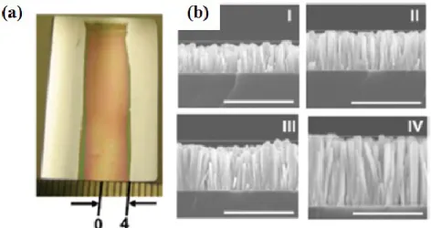
Figure 1.29: (a) Image of a sample ZnO NRs on a Si substrate patterned with an ∼8
mm wide strip of ZnO seeds in the middle of the substrate. The darker part of the substrate is where the nanowires have grown and the lighter parts are unseeded regions where there are no NRs. (c) Cross-sectional SEM images of the NRs array at different locations between the positions 0-4 indicated in (a). Adapted from [105].
As further confirmation, the mass transport limitation was proved to be responsible to the non-uniform growth in the area between seeded and unseeded regions. A Si substrate was patterned and seeded only in the middle of the substrate, leaving the rest of the surface unseeded. Consequently, ZnO NRs grew only in the middle of the substrate (Figure 1.29(a)). Figure 1.29(b) shows cross sectional SEM images at various points between the position 0-4 labeled in Figure 1.29(a). Moving towards the unseeded region, NRs height increases because ofthe higher ZnO precursor concentration near the boundary between the seeded and unseeded regions. Finally, Boerker et al. confirmed that the anisotropic growth of ZnO NRs is not driven by the mass transport growth but by the growth kinetics of (0001) and (101̅0) planes of ZnO in the considered synthetic conditions, as already verified also by other authors [106].
1.5
ZnO Nanowalls: a brand new material
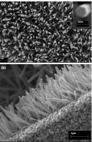
The effect of the substrate on the nature of the ZnO nanostructure formed via CBD was extensively studied [85]. It was observed that the usual shape assumed by ZnO, in chemical bath containing zinc nitrate and HMTA, is the nanorod one. However, as the substrate is Al or Al covered wafer, a particular 2D morphology of ZnO is formed, named usually nanowalls (NWLs) consisting of ZnO crystalline foils. ZnO NWLs (or nanoplatelets) grow vertically on Al substrates, with an intertwined, random, honeycomb-like pattern and c-axes parallel to the substrate. The first study of ZnO nanowalls was reported by Ng et al. [107] through carbothermal reduction (thus not a CBD method) for growing vertical ZnO nanowalls on a sapphire substrate, Figure 1.20.
Figure 1.20: ZnO nanowalls grown by carbothermal reduction on sapphire with a
height of 5µm. Adapted from [107]
As in the case of ZnO NRs, NWLs can be prepared by both physical and chemical vapour deposition techniques, with operating temperatures higher than 800 °C [108, 109]. Alternatively, ZnO NWs can be easily synthesized on Al-covered substrate by CDB at 90 – 100 °C [110-112]. However, in contrast to the case of 1D ZnO NRs, ZnO nanowall structure has not been investigated as much, although its huge surface-to-volume ratio and extremely thin wall thicknesses pave the route for many interesting applications [108,110- 112]. Ye et al. [110] reported the synthesis of ZnO NWLs on Al wafer in an equimolar solution of zinc nitrate hexahydrate and HMTA. For comparison, they produced ZnO NRs on Si substrate, using the same growth solution, as presented in Figure 1.21.
It is reasonable to assume that the presence of Al in the substrate is important for obtaining ZnO NWs, since the growth suppression effect along [001] direction can be originated from Al. Indeed, aluminum is an amphoteric metal and it can dissolve in the alkaline conditions. Therefore, in aqueous solution containing HMTA, Al undergoes chemical reaction, forming Al (OH)4 –, as follows:
2Al(s) + 6H2O + 2OH- 2 Al(OH)4- + 3H2 (1.6)
These Al complexes bind to the Zn2+ terminated (0001) surface and
Figure 1.21: SEM images of nanostructures grown by CBD. (a) ZnO nanowalls at
low magnification and higher magnification (inset); (b) ZnO nanorods arrays. Adapted from ref [110].
Ye et al. [110] demonstrated that by increasing pH from 6 to 12 (by adding ammonium hydroxide, AH), thinner nanowalls could be obtained. Changing the pH value of the solution alters the concentration of Al(OH)4- in
the solution as well as its adsorption quantity and coverage rate [110]. Moreover, NWLs of Zn-Al carbonate hydroxide hydrate, a layered compound, and ZnO nanorods were obtained at pH 10 with zinc acetate,
ammonium hydroxide, and e-beam evaporated Al film [113]. The concentration of Al(OH)4- influenced the particular product obtained; at high
concentration of the Al complex, made possible by using a 1 µm Al film, only the Zn-Al carbonate hydroxide hydrate NWLs were obtained, while a 100 nm Al film gave the layer compound first, and later ZnO nanorods on top. The authors attributed the formation of ZnO nanorod to the exhaustion of Al(OH)4- needed to ensure the NW morphology. Therefore, it is clear that
the growth rate of ZnO NWLs can be controlled by manipulating the rate of Al(OH)4- generation that can be enhanced by increasing the pH of the
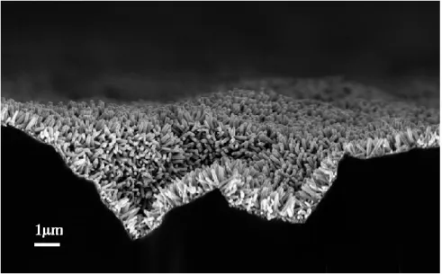
solution. Moreover, starting from a solution of HMTA and zinc nitrate, a fast (10 min) sonochemical route for ZnO NW growth on Al and alumina substrates (with) at ambient conditions was reported by Nayak et al.[114]. However, there is no information on whether the growth dynamics and film quality differ between the two substrates. Moreover, prolonged sonication caused the NWs to peel off. ZnO NWLs can be also obtained by the selective etching of dense ZnO NRs films grown by CBD [115]. The process consists in three steps: the formation of a ZnO seed layer, the growth of ZnO NRs in an equimolar solution of 0.1M zinc nitrate and HMTA at 75°C and, finally, the etching into 0.3M KOH aqueous solution. The defect-selective dissolution in (0001) planes and along the c-axis, caused by the preferential adsorption of OH- on particular faces, drives the formation of nanowall
structure. Figure 1.22 shows etched ZnO NWLs and the initial NRs film. At present, a complete picture of formation process of ZnO NWLs on Al substrate as well as an effective way to control the growth, have not yet been achieved.
Figure 1.22: SEM images of (a) dense ZnO NRs film grown by CBD; (b) etched
ZnO NWLs at different magnification. Adapted from ref [115].
Chapter 2
ZnO Nanorods Growth by Chemical Bath
Deposition
ZnO nanorods grown by CBD are among the most promising
semiconducting nanostructures currently investigated for a variety of
applications. As a consequence, many works have been devoted to
deeply understand the microscopic mechanisms leading to high aspect
ratio and vertically aligned ZnO NRs. Still, contrasting experimental
results appear in the literature.
This chapter presents a systematic investigation of the chemical
deposition of ZnO nanorods using zinc nitrate salt and
hexamethylenetetramine (HMTA). An optimized procedure for
reproducible synthesis is presented as well as the growth kinetics is
discussed. In addition, an empirical study evidences the double role of
HMTA in the NRs growth mechanism. HMTA is shown to participate
both as a supplier of OH
−ions and as a capping agent promoting the
anisotropic growth. These two actions are not mutually exclusive and
the amount of HMTA in solution determines the key process variable.
This represents a promising step towards a better control of CBD
synthesis.
2.1
HMTA, the key player
In recent years the possibility to fully exploit the advantages of CBD of dense arrays of zinc oxide NRs has stimulated detailed studies. Significant progress has been made in investigating the growth mechanisms, nevertheless the interpretation of the obtained results has been often matter of discussion. In particular, the role of HMTA in the growth kinetics is currently under debate and in this regard the literature proposes some contrasting interpretations. HMTA is a tertiary amine highly soluble in water, having a symmetric tetrahedral cage-like structure with four nitrogen atoms (N) at the four corners and six methylene bridges (-CH2-) as shown in
Figure 2.1. It is the most used ligand in the chemical bath deposition of zinc oxide nanostructures.
Figure 2.1: Chemical structure of HMTA. Adapted from ref. [116].
Many works have reported on the slow hydrolysis of HMTA in formaldehyde [CH2O] and ammonia [NH3] in the range of temperature and
pH values involved in CBD [87, 92, 102, 117, 118]. Therefore, HMTA gradually releases the hydroxide ions driving the formation of ZnO (see Equations 1.1-1.5 in Chapter 1); at the same time, it controls the pH solution [85]. Ashfold et al. [92] have reported that the rate of HMTA decomposition at 90°C calculated for a zinc-free solution is the same of that observed experimentally in a solution containing zinc nitrate, implying that HMTA decomposition does not depend on the reactions taking place during ZnO formation and that HMTA is an effective pH buffer. Furthermore, HMTA or
other ammonia ligands can bind to the free zinc ions in solution, forming metal complexes and keeping the Zn(II) concentration under control [85, 93]. It is worth noting that the presence of HMTA in not essential for the ZnO nanorods growth [85, 116, 119] but it ensures crystalline and morphological properties better than other alkaline agent [Govender2004]. Near thermodynamic equilibrium, the driving force for the growth of wurtzite structured ZnO NRs is the minimization of the free energy of the system, as described in the Section 1.4. The elongated ZnO crystals are characterized by higher energy polar c-planes (with the alternation of Zn2+
terminated and O2- terminated surfaces) and by non-polar lateral facets
having lower surface energy. The fact that the anisotropic growth of these nanostructures is intrinsic to wet chemical methods and to wurtzite structure has found several experimental evidences [55, 105]. However, these thermodynamic considerations are not sufficient to explain the wide variety of nanostructures and the role of the bath composition on the growth rate of polar and nonpolar crystal plane must be taken in account [55, 120].
Even if HMTA decomposition is assumed in most papers [117, 121], Sugunan et al. [122] first have proposed that HMTA does not degrade during CBD of ZnO NR. They used attenuated total reflection Fourier transform infrared (ATR-FTIR) spectroscopy performed on a mixture of 0.1 M HMTA and zinc nitrate upon continued heating, and revealed no change in the tertiary amine structure. As shown in Figure 2.2, the absorption peak at 1012 cm-1, (stretching vibrations of C-N bonds of HMTA) was monitored at
different times. If thermal decomposition of HMTA into formaldehyde and ammonia had occurred, a significant reduction of the absorption signal would have been detected. Only a negligible degradation of the tertiary amine has been revealed by infra-red spectroscopy, although the anisotropic growth of ZnO was observed within 5 hours.
Figure 2.2: ATR-FTIR spectra for a solution of HMTA and zinc nitrate kept at
65°C for 1, 2 and 5 hours. Adapted from ref. [122].
They have also suggested that HMTA molecules, being non-polar chelators, are able to attach the non-polar surfaces of the nanorods acting as a capping agent for these facets and propelling the anisotropic growth along the c-axis, Figure 2.3.
Figure 2.3: Illustration of the possible role of HMTA in the anisotropic growth of
Such shape-inducing effect of HMTA has been recently refuted in 2014 by McPeak et al. [116], who have claimed that ZnO nanorods growth by CBD does not involve the adsorption of HMTA on the ZnO lateral faces and the role of HMTA is only to control the saturation index of ZnO through the slow release of hydroxide ions.
Figure 2.4: Time resolved ATR-FTIR spectra during the adsorption study of 1mM
HMTA in 25mM KCl on ZnO nanoparticles. Adapted from ref. [116].
Figure 2.4 reports the results of in situ ATR-FTIR analysis performed by flowing 1mM HMTA in 25mM KCl solution on ZnO nanoparticles film for 60 minutes, followed by 10 minutes of rinsing with an aqueous solution of KCl. After 5 minutes the peaks at 1012 and 1238 cm-1 appeared,
corresponding to C-N stretch and CH2 rock respectively. Moreover, the peak
positions and intensities did not change within 60 minutes while all the signals disappeared after 10 minutes of rinsing. McPeak et al. interpreted these data as coming from the solution phase rather than as indicating HTMA adsorption on ZnO.
Both works of Sugunan and McPeak are based on the results of attenuated total reflection Fourier transform infrared spectroscopy that, actually, allows to investigate the solid-liquid interface with high sensitivity.