2
INDEX
I- Introduction…..…….………..………....
pag. 3Organic molecules for functional applications: Solar cells...pag.3
II- Aim of the research……….……….…...
pag. 18III- Results and discussion……….………..
pag. 23III- 1 Synthetic route to the polymer ...…………..……….….pag. 23 III- 2 NMR evidence for polymer assembly.……….….………....pag. 29
III- 3 UV-vis and Fluorescence spectra of the new polymer………....…...…...pag. 34 III- 4 Electrochemical measurements……….pag. 39 III- 5 Developing the simulating device………..pag. 40 III- 5a AFM Measurements on PCBM and Polymer- modified surfaces ………...pag.45 III- 5b XRR Measurements on organic layers ……….………....pag. 49 III- 6 Electrical measurements………....pag. 51 III- 6a Sheet Resistance measurements of PCBM and different polymer layers...pag.52 III- 6b I/V measurements on different layers of PCBM and P3HT...pag.55 III- 6c I/V measurements on different layers of Polymer, PC[5]net and PC[5] cap
deposited on n-Silicon and p-Silicon...pag.57
IV- Experimental……….
pag. 62Synthesis of
5,11,17,23,29-pentat-butyl-31-benzyl-32,33,34,35-tetrahydroxycalix[5]arene(2)...………....…....pag. 62 Synthesis of 5,11,17,23,29 pentat-butyl-31-benzyl-32,33,34,35-(4-methylpentyloxy)
calix[5]arene (3)………...…….………....pag. 64 Synthesis of 5,11,17,23,29 pentat-butyl-31-monohydroxy 32,33,34,35
(4-methylpentyloxy) calix[5]arene (4)……..…..……….…………pag. 66 Synthesis of 1,4-bis (4-methyl pentyloxy)-2,5-diiodo benzene (10)...pag. 68 Synthesis of 1,4-bis[(Trimethylsilyl)ethynyl]-2,5-bis-(4methylpentyloxy) benzene (11)...pag.71 Synthesis of 1,4-Diethynil-2,5 bis(4-methylpenthyloxy) benzene (12)...pag. 74 Synthesis of 1-4Bis[6-chlorohexyloxy]-2-5Diiodobenzene (8)...pag. 77 Synthesis of bis calix[5]arene (9)...pag. 80 Synthesis of polymer PC[5]...pag. 84 NMR Titration polymer/diammonium picrate……….…….…………..….…pag. 88 Fluorescence Titration polymer/diammonium picrate………….……….………pag. 89 Acid-Base Effect on Fluorescence of PC[5]net……….…...pag. 91 Acid-Base Effect on Fluorescence of PC[5]cap………..……….pag. 92 Electrochemical measurements...pag. 93 General procedure for spin coating of different organic solutions...pag. 94
V- Conclusions………..………..
pag.101VI- Bibliography………..…………...….
pag. 1033
I.
1- INTRODUCTION.
Organic molecules for functional applications: solar cells
The efforts on studying a system that could convert light in electrical Energy started in early 1970’s in order to reduce the environmental impact of fossil fuels and to offer an alternative to the dangerous nuclear power.
A solar cell is a device that can use the photoelectrical effect (discovered by Baquerel in 1839) to convert light in a lasting current, so it acts as an electrical generator.
In a solar cell the “photogenerated” electrical charges are separated basing on their sign and then collected by two electrodes having different potential. Today’s solar cells are realized using various materials and many structures, but solar cells belonging to the first generation, based on p-n junction, are the most efficient and the most diffused in the global market.
In Silicon-based solar cells the n- or p- doping is related to the introduction of an extra-band between the Valence band and the Conducting band belonging to the Silicon.
This treatment is made in order to obtain a constant electrical current in a cell, thanks to the introduction of an Electrical Field.
In case of p- doping, some impurities (e.g. Boron atoms) are introduced in Silicon’s crystals; as a consequence, an empty band is introduced in the Energy gap between the Valence band and the Conducting Band of Silicon. After absorbing a photon having the suitable Energy value, electrons can cross the gap between the Silicon’s valence band and the new “implanted” band.
The same mechanism is at the basis of n-doping; in this case, an extra band full of electrons is introduced thanks to the implantation of P atoms in Silicon’s crystals. In this case electrons can be promoted from dopant’s full band to Silicon’s conducting band.
4 Obviously, when an electron moves from a band to another, it leaves a “hole”, an empty space that can be filled by another electron. In the recombination process, every free electron can join a hole thus returning a part of its energy to the system in form of heat.
If we consider a Silicon Crystal, when the p-doped and the n-doped zones are joined, the interface between the 2 materials is called p-n junction. An electron transfer from n- to p- due to the majority carriers happens at the interface between the crystals, and obviously a hole transfer from p- to n- happens at the opposite. This behaviour determines at the p-n interface a depletion zone, having a double layer of opposites charges and no free charge.
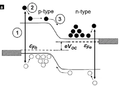
The lighting of the p-n junction generates an exciton. After that, an Electrical field at the depletion zone (called “built in field”), separates the electrons from their holes and force them to the n- zone (the electrons) and the p- zone (the holes).
After that, minority carriers (the electrons in the p-, the holes in the n- material) diffuse to the junction, from where they are swept away, so they accumulate on the other side of the junction, where they become majority carriers (step 1, 2 and 3 in part a in Figure 1).
Figure 1. The process of separation, diffusion and accumulation of charge carriers in a simple p-n
5 This knowledge allowed to develop different varieties of devices based on Silicon; in particular, we can distinguish:
- Amorphous Silicon-based systems - Polycristalline Silicon-based systems
At today, amorphous Silicon-based systems reached the 15% maximum efficiency in converting light in electrical power, while polycrystalline Silicon-based systems have reached more than 20% maximum efficiency.
Although the good performances in terms of efficiency, maybe one of the most important reason for the lack in widespreading the solar cell’s technology is the cost of the solar panels themselves, and the cost of installation, which represents approximatively half of the total prize of a domestical solar implantation.
The research of cheaper materials that can be used in industrial processes is a possible solution to this problem; in alternative a new industrial process to obtain the same device in a cheaper way could be elaborated.
This consideration has led to the development of devices based on Cadmium Telluride (CdTe) and Copper Indium Gallium Selenide (CIGS), which represent the second generation of thin film technologies because they can be manufactured by roll-to-roll processes. These processes have the advantage to be cheaper to manufacture than crystalline silicon and, as a consequence, they lead to lower electricity costs, which are extimated to be around $1-2/Wp at high productions volumes and efficiency (5-12%).
Since 1980’s, thanks to the development of the first Organic Thin-Film Transistor (OTFT’s), organic materials (both polymer- and small based molecules based devices)1-3 have attracted scientific interest in the field of electronics.
Organic materials are used as charge carriers in a variety of potential applications, spacing from optoelectronics to electrochemical devices, such as Organic Light Emitting Diodes (OLEDs), sensors, electrochromic devices and Organic Field Effect Transistors (OFETs).
6 Molecules having a conjugated system are promising materials for photonic applications since their inherent dipole enhances the nonlinear optical response properties of the material.4-5 In fact, the presence of a π- electron system in a molecule allows it to absorb sunlight; after that “photogenerated” charge carriers are created and then they can run across the material.
In general, organic semiconductor can be classified as “intrinsic wide band gap semiconductors” (band gap above 1.4 eV) down to “insulators” (band gap above 3 eV) with a negligibly low intrinsic charge carrier concentration at room temperature in the dark. Chemical, photochemical or electochemical doping can be used to introduce extrinsic charge carriers into organic semiconductors. For example photoinduced electron transfer from a Donor- to an Acceptor-type molecule can be used to introduce free charge carriers.6
Unfortunately, low charge mobility hindered the developing of practical applications of these materials. Nevertheless, organic materials are potentially advantageous respect to the inorganic counterparts because of the possibility to develop a low cost synthesis, the possibility to manufacture thin devices by common surface modification methods, or the possibility to create flexible devices that can be produced in large scale at relatively low cost.7
In 1991, thanks to the development of the Gratzel’s cell,8 chemists returned on organic solar cell’s development thanks to the concept of Dye Sensitized Solar Cell’s (DSSC).
The Gratzel’s cell is composed by of two parts, an organic molecule (a metal iridium or platinum complex) is covalently bonded to a inorganic support of TiO2. (Figure 2)
The organic complex acts as light-harvester; it absorbs a photon and after that it starts the formation of an exciton (an anion or cation radical) that can be transferred to the titanium oxide. Obviously, in this red-ox process the organic molecule has to re-generate its oxidation state, so this system needs to take place in a medium (a solution) containing in the most of cases the I-/I2 couple.
7
Figure 2. The Gratzel’s cell scheme
Despite the fact that, at today, Gratzel system is the most efficient organic-inorganic hybrid system because of the broad spectral range of absorption due to the inorganic semiconductor, this kind of “hybrid” cells has the great disadvantage of needing an electrolytic solution in order to regenerate the oxidation states of the molecules involved in the process. The use of a solution implies some technical difficulties to develop efficient cells because of the risk of leaks in the device, corrosion and the impossibility to realize flexible solar cell.
Moreover, from a performance point of view, Gratzel’s cells are far from Silicon cells in terms of performance, in fact the best laboratory cell reaches the 10% maximum efficiency under illumination, with module efficiencies ranging from 3% up to 5%.9 Another disadvantage is the request of a broad light absorbing spectra organic molecule in order to act a very efficient light harvesting.
The amount of light that can be absorbed by a single monolayer is poor because the area occupied by a single molecule is much larger than its optical cross section for light capture. Thus, to improve the photovoltaic efficiency it’s better to use a porous, nanostructured film of very high surface instead of a flat one. The principle is similar to what that happens in leaves, where the thylakoid vesicles are stacked in order to improve the light harvesting of chlorophyll.10
Another technology connected to the use of carbon-based molecules is known as Organic Photovoltaics.11 In this case a solution containing the organic molecule is
8 used to modify a surface thanks to printing or coating techniques. The drying of the solvents allows to deposit the organic molecule on the surface and to obtain a solid state photovoltaic device.12 This is a valuable approach because of the possibility of using simple, high speed and large scale manufacturing processes.
The key feature to explain how a OPV cell works is the mixture of n-type and p-type charge carriers in the active layer that is used to modify the surface.
Obviously, as organic molecules are the effective actors of charge-carrying, it’s not convenient to explain charge transfer in terms of band structure, but in terms of frontier orbitals, so it’s better to talk about HOMO (High Occupied Molecular Orbital) and LUMO (Low Unoccupied Molecular Orbital) instead of Valence band and Conducting band.
Organic molecules can withdraw or donate electron or holes; for the sake of simplicity we will talk about Electron-Withdrawing and Electron-Donor molecules; an Electron-Donor (D) molecule has low Ionization Potential and thus a high lying HOMO energy, an Electron-Acceptor molecules (A) have a high Electron Affinity (EA) and, as a consequence, a low lying LUMO Energy. The charge transport happens at the interface between D and A.13
The acceptor specie (the n-type molecule) must have a lower LUMO level respect to the donor molecule in order to have a higher probability to verify the charge transfer instead of the return to the ground state.
9
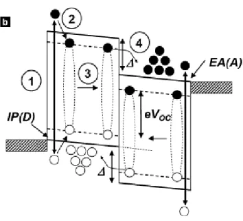
Figure 3. Different steps during the interaction between a Donor and an Acceptor Organic Molecule
involved in a solar cell.
After absorbing a photon, whose energy is larger than the gap between HOMO and LUMO, there thermalization of the holes and electrons near the top of valence and conduction band respectively happens.
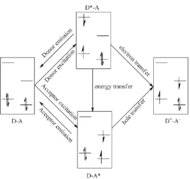
In the organic junctions part of this process is similar to that described in Fig.1. In fact, after the absorption of a photon, we have the formation of excitons that diffuse in the heterojunction (step 2 and 3 in Fig. 3), where they dissociate and transfer a electron (or a hole) into the acceptor (or donor) layer (step 4 in Fig. 3). This isn’t the only pathway that can be followed; the deactivation of the donor exciton (through the Forster energy transfer) leads to the acceptor’s excitation; after that, the quenching caused by charge transfer can happen. When the acceptor core is excited, there is a hole transfer moving the hole from the HOMO of the acceptor to the HOMO of the donor can happen. This can lead again to a non emissive charge separated state. Thus, no matter if the donor or the acceptor specie is excited, photoinduced electron (or hole) transfer follows that quenches both the donor and the acceptor fluorescence and leads to a non-emissive photoinduced charge separated state. (Fig.4)
10
Figure 4. Possible patways that can be followed by the couple Donor-Acceptor Molecule after a
photon’s absorption.
The physical behaviour standing at the base of this phenomenon allows, in principle, a possible all-organic solution to the photovoltaic device development. It could be thought to synthesize organic molecules acting as light harvesters in order to form excitons (charged species having an uncoupled electron).14
This kind of solution could make chemists able to develop cheaper and more flexible solar cells, but a crude approach to this problem leaves several points to take care.
In fact, in order to convert the most of the light in electrical energy, the molecule acting as light harvester has to absorb the widest visible spectrum as possible, and most of the organic semiconductors investigated today absorb in the visible range, while sun has its maximum photon density at around 700 nm; moreover organic molecules have an intrinsic limited durability because when electrons are excited to higher molecular orbitals, anti-binding states arise and the probability for decomposition of the compound increases.15 Moreover, an efficient light harvesting process needs not only a Donor-Acceptor interface, but an efficient charge separation and transport. These two features may be guaranteed by the continue
11 interface between Donor and Acceptor and by a continuous path for the transport of separated charges to the contacts. These are the conditions allowing light harvesting to happen in ultrafast-time scale in order to obtain separated charges that could be collected by the electrodes in form of a current that could be measured. 16
This is a master point for the Gratzel’s cell, but in order to allow a better industrial scale up, scientists have tried to develop systems based on the use of blends17 of acceptor (n-type dopants) and donor (p-type dopants) molecules.
These devices were based on simple blends of Fullerenes and P3HTs, but the results were poor respect the theoretical calculations.18 In fact these molecules have a poor reciprocal solubility, so they tend to segregate themselves after some time, so the exciton’s formation can happen only at the interface between the acceptor and donor layer. Obviously this is an aspect limiting the photoconversion, the efficiency and the durability of the cell. To the best of our knowledge, the best results in terms of photoconversion were obtained by Heeger and Guo, recording over the 5,5 % as efficiency.19-20
Maybe the most simple solution to this problem was binding the acceptor molecule to the donor one thanks to the organic synthesis and, in order to rise the solubility of the product molecule, using, for example, the oligomeric species of the P3HT
instead of the polymer.21-22
This kind of solution is very attractive respect to the use of polymers in terms of tailoring structures and obtain desired features (e.g., energy levels, absorption spectra, charge-carrier mobility, purity), but it is limited by the low reproducibility of the results, as the interactions between the active layer are not easily predictable, moreover, despite the better solubility, the results even in these case are very poor, compared to Silicon based solar cells, because of the difficulty of organic molecules to absorb the whole visible spectrum. To our knowledge, Nierengarten et al. were the first to attempt this approach, binding the PCBM with π-conjugated systems, both vinylene- and acetylene like. 23
12 Conjugated polymers have been investigated extensively for their applications in optoelectronic devices, such as light emitting diodes, photovoltaic cells, OFET, sensors.24 Their performances in optoelectronic devices is determined mainly by interchain interactions, rather than by intrinsic properties of the conjugated polymer.25 In order to control and take advantage of their interchain behaviour, conjugated polymers or oligomers have been introduced in a rod-coil block copolymer architecture as the rod component.
Many efforts were made to enlarge as much as possible the absorption spectrum of molecules by using pigments.26 Even in this case the pigments can be linked to fullerene or thiophene-based molecules thanks to organic synthesis, but the values obtained and the not so appealing possibilities to make an industrial scale up have limited this approach.
In order to act these applications, electron donating and electron accepting properties of the molecules are of crucial importance.
From a molecular point of view, the target molecule has to be high-conjugated in order to act the charge transfer in a long range between the electrodes. Moreover, depending on the application, a broad absorption spectra in the visible region could be required. Obviously, from a chemical point of view, a focus parameter is the solution processibility in order to do further syntheses.
From a structural point of view it’s better to achieve further progress concerning the supra-molecular control of the active layer morphology, i.e., by hydrogen or halogen bonding, exploiding the rigid rod-like structure of monodisperse molecules.
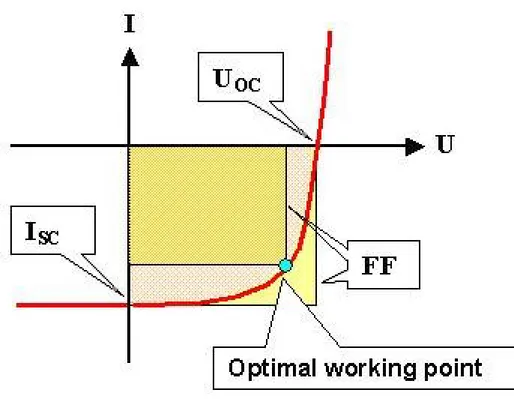
13 Voltage-current (V-i) measurements are needed to describe the performances of a solar cell. Fig.5 shows a tipical I-V plot under dark and light conditions. We can obtain many informations about the parameters describing a solar cell.27-28
- The open-circuit Voltage (VOC).
It is the Voltage that has to be applied to make the current be equal to zero. It depends by the energy levels’ offset of the used materials as well as their interfaces.
- The short circuit current (ISC).
It is the current flowing when the Voltage is equal to zero. This parameter depends by the nanoscale morphology of the organic semiconductor thin film. In a van der Waals crystal, the final nanomorphology depends on film preparation, so experimental parameters as solvent type, the solvent evaporation
(crystallization) time, the temperature of the substrate and the deposition method can change the nanomorphology. In BHJ there is an enhanced interfacial area between donor and acceptor phases, but this factor is counterbalanced by a complicated nanomorphology that is difficult to control.
- The maximum power point (PMAX). It correspond to the maximum
product between Voltage and current. - The Fill Factor (FF).
It is the ratio between the PMAX and the maximum Power that could be obtained (
the product between ISC and VOC).
MAX
SC OC
P
FF
I
V
The Fill Factor depends by the charge carriers reaching the electrodes, when the built in field is lowered toward the open circuit voltage. In fact, as just said, there is a competition between charge carrier recombination and transport. Hence, the
14 product between the lifetimes times the mobility determines the distance d that charge carriers can drift under a certain electric field. This product μ*τ has to be maximized.
- The Internal Quantum Efficiency (IQE).
It is the ratio between the PMAX and the short circuit current ISC.
MAX SC
P
IQE
I
- The External Quantum Efficiency (EQE). It is the ratio between short circuit current ISC and the forced current IF.
SC F
I
EQE
I
- The efficiency of the solar cell as a ratio between the PMAX and the
incident solar power PINC.
MAX INC
P
15
Figure 5. I-V curve showing solar cell’s main parameters.
The efficiency, however, it’s the best way to compare solar cells between them because it indicates how many incident Energy is really converted in Electrical Energy.
In Organic Photovoltaic (OPV), the short diffusion length of donors (less than 10 nm), which is much shorter than the optical absorption length (100 nm),29 has limited the EQE, and a large fraction of photogenerated charge remains unused for photocurrent generation. Therefore, it is crucial to control the of the morphology and of the mixing state of the Donor-Acceptor heterojunction.
Concluding, several approaches can be applied to improve the efficiency of organic solar cells. These can be reduced to the regulation of two factors:
a- Regulation of the band gap of organic molecules in order to improve electrical parameters as Voc and Isc
16 b- Regulation of the morphology of the films in order to minimize the losses by recombination of the wrong sign of charges at the wrong electrode. In this sense, organic molecules are very versatile because the band gap can be regulated by “tailoring” the opportune synthesis.
The nanoscopic organization can be regulated by introducing
1- An amphiphilic primary structure like di-block copolymer resulting in a self-organized phase;
2- An amine-acid- type hydrogen bonded self organization resulting in a hydrogen bonded polymeric superstructure
3- An inorganic (ZnOx or TiOx) template nanostructure filled with organic
semiconductors
4- Liquid crystalline self-organizing columns of donor-acceptor phases. This strategies require a multi-discipline knowledge in macromolecular chemistry, supramolecular chemistry, physical chemistry, colloid chemistry, photophysics/photochemistry, device physics, nanostructural analysis and thin films technology and, as consequence, great challenges and advancements in the entire field of chemical sciences.
In particular, if we consider a non-covalent approach, supramolecular polymers appear to be interesting because of the possibility of tunable structural properties arising from the dynamic linking between the constituent monomers.
If we consider chemical sensors, it’s well known that the aggregation state of the receptor could influence its ability to convert the chemical information in an electrical signal. The same approach could be thought if we consider the organic materials to be used in photovoltaic cells. In case of polymers, we can approximate them as presenting the exciton with a one dimensional diffusional pathway. The excitons therefore undergo a one-dimensional random walk when the polymers are in solution. If the exciton can undergo vectorial transport in a given direction, then much higher amplification factors can be achieved. The situation is more complicated in polymer films. Close proximity of the neighboring polymer chains
17 facilitates interchain energy migration, and fluorescent polymers often exhibit more planar conformations in thin films and aggregates, which appears to promote exciton diffusion.30 As a results, the research of new methods to aggregate fluorescent polymers into optimal organizations for energy transfer is a great chance for investigations.
18
II. AIM OF THE RESEARCH
The target to be reached with this project is the development of a new organic molecule acting as organic dopant and, in a second moment, developing a photovoltaic system at the solid state that can be a suitable alternative to the commercial solar cells.
These new devices are based on using thin or ultrathin layers of organic molecules (having a π conjugated electron system) acting as n- and p- dopants . These molecules have been proved to have good electronic properties in solution because of their Molecular Orbitals offset that make them suitable for Organic Photovoltaic applications.
Chemical features as the presence of an appropriate alkyl chain may influence the consequent intermolecular interactions, and thus can can be used even to improve the solubility of the molecule in organic solvent, its homogeneity and finally the cristallinity of the organic layer. In this way we expect to obtain better values of photoresponse respect to the systems used as models.
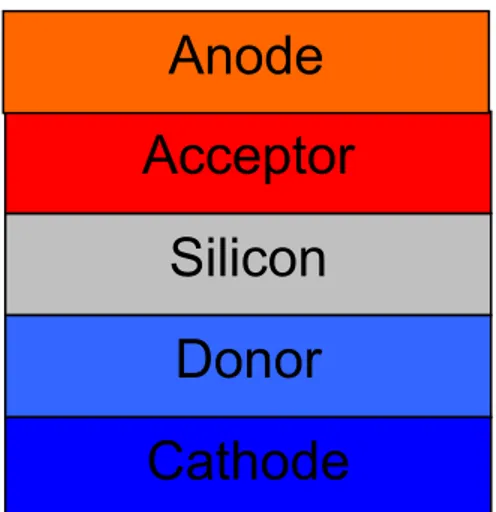
Figure 6 : Scheme of device’s conception. The Silicon surface acts as light harvester. The donor and acceptor
molecule act as molecular wires to anode and cathode thanks to Molecular Orbital’s tuning, that allows a continue electron transfer between HOMO an LUMO orbitals.
Literature is rich of examples in which organic molecules act as light harvester both as a blend of electron-donor and electron-acceptor molecules layer and a dyad
Silicon
Acceptor
Donor
Cathode
19 layer (in this case a single molecule has both the acceptor and the donor properties).
At the best of our knowledge, there are few studies regarding organic compounds interacting with Silicon, Stutzmann et al. tried to study the interaction between nanocrystalline Silicon or hydrogenated amorphous Silicon with organic molecules, where it has been observed a little photovoltaic effect.31
A photovoltaic system based on inorganic semiconductor could be promising for several reasons. In fact inorganic semiconductor have a much broader absorption spectrum than organic semiconductors, moreover they can be doped to a specific n- or p- type doping level, and (expecially in form of nanocrystals) they can provide a large interface area to the organic counterpart. system based on intrinsic Silicon acting as light harvester that can be implied in the electron transfer process to an acceptor molecule and an acceptor molecule to close the circuit.
The work consists in synthesizing a new molecule, recognizing its band offset and match it to the band offset of Silicon32 in order to improve the charge transfer, thus achieving higher values of photocurrent.
The new molecule that will be studied belongs to the family of PolyPhenyleneEthynylenes (PPEs), in which aryl groups are linked by alkine units and their derivatives. Because of the molecular properties, compounds belonging to this class turned to be suitable candidates for improving the performances of OPV solar cells respect to the poly-phenylenevinilenes and polythiophenes, so in the last years there have been a rise of interest respect to this conjugated polymers.33
The electronic properties can be modified by introducing appropriate substituents in order to regulate the HOMO-LUMO levels and consequently the band gap between the valence band and the conductive band of the organic molecules.
For most conjugated polymers, when the conformation of a chain passes from a “twisted” into a relatively planar one, the π electron delocalization along the backbone would become easier, and hence the spectra would red shift to a certain extent. 34 This result can be reached through the introduction of suitable
20 ramifications and the use of spacers allowing both π delocalization and steric rigidity.35
In addition, the rigid acetylenic spacer helps to minimize neighboring aromatic-ring interactions in this series should result in a bathocromic shift in the UV-vis absorption spectra maxima with corresponding reduced bandgap energy when compared to polythiofene or polyalkylthiophene analogues.36
The presence of triple bonds as spacers can even regulate the interactions between different polymeric chains. It has been found that the intrachain effect is extremely strong for PPEs, owing to the relatively low rotational barrier of the aryl alkine single bonds along the backbone, which is extimated at less than 1 Kcalmol-1. On the other hand the backbone planarization will give rise to a closer interchain contact, that will give rise to a closer interchain contact, which in turn facilitates the formation of the aggregates in the most of circumstances.37
Although these possible advantages, at the best of our knowledge, there isn’t any example in literature attesting the effective use of PPEs polymers in working OPV devices.
In order to analyze the behaviour of the new molecule, as well as to develop the new photovoltaic device’s architecture, the first step was testing a model device based on well known organic molecules acting as photovoltaic materials. At today, molecules belonging to the Fullerene family and to the p-thiofenes are the most used in this field of the research.
The most used donor molecules belong to the Poly-3-Exyl Thiofene (P3HT) or the poly-p-phenylene vinylene (PPV) family because of the possibility to form well-ordered structures at the solid state. These polymers allow us to achieve many advantages, in fact the chainlike structure leads to strong coupling of the electronic states to conformational excitations peculiar of the one dimensional systems, moreover the relatively weak interchain binding allows diffusion of dopants molecules into the structure (between chains) while the strong interchain C-C bonds keeps the integrity of the polymer.
21 Because of their good solubility, good processability and environmental stability we choose P3HT as reference molecule to test the behaviour of the new synthesized compound and the developing of the device having a new architecture.
As a model for exploring the properties of this device [6,6]-phenyl-C61- butyrric acid methyl esther (PCBM) will be used as n-type dopant because of its ability to accept up to six electron in its conduction band.38 In turn, poly-3-hexylthiofene (P3HT), one of the most representive conjugated polimer donor material will be used as p-dopant.39
[6,6]-phenyl-C61- butiric acid methyl esther (PCBM), is a well known n-type molecule. It can be syntehesized starting from fullerene C60 by using
1-phenyl-1-(3-(methoxycarbonyl)propyl)diazomethane40 , the phenyl butyric methyl esther moiety make it soluble in common organic solvents. PCBM maintains one of the most attractive features of C60, which is its long electron diffusion lenght, that is longer
than Perilene carboxy diimide derivatives. This property is due to the rapid intersystem crossing of the singlet excited state to the long lived triplet excited state, allowing ample time for its diffusion.41 The absorption spectrum of C60 is reported in
Fig. 7.
Fig. 7. Absorption Spctra for PC61BM (green line) and several other molecules used for photovoltaic
22 As we can see, the negligible absorption in the visible and infrared spectrum is attributed to a high degree of symmetry, making the lowest-energy transitions formally dipole forbidden. It has been proved that reducing the symmetry, by replacing PCBM with a less symmetrical or elliptical fullerene (as PC71BM) these
transiction become allowed and a dramatic increase in light harvesting is expected. Therefore, the PCE in many solar cell devices has been enhanced by using C70
derivatives as the acceptor material. Unfortunately, C70 derivatives are more difficult
and expensive to separate, so C60 ones are still used.
This feature, mixed to the stability of blends with P3HT, the good alignment between HOMO and LUMO orbitals and the fact that at today PCBM is commercially available should encourage the use of these blends in commercial device; unfortunately PCBM high price and the natural tendence of fullerenes to photooxidation is a real limit to a large scale use. Moreover, lower-lying LUMO Energy level in PCBM reduces the VOC, which is determined between the HOMO
23
III- RESULTS AND DISCUSSION.
III- 1 SYNTHETIC ROUTE TO THE n-TYPE ORGANIC MOLECULE
In recent years there have been an increasing interest in synthesizing conjugated polymers and in studying their photoluminescence and electroluminescence properties.42
These molecules can sum the processability of organic materials and the electronic and photophysical properties of semiconductors, so they are attractive candidates as active layers for electroluminescence devices.
Polymers belonging to the p-phenylenethinylene family are particularly attractive because of their flexible molecular orbitals energetic, known to be tunable via an appropriate skeletal functionalization. Moreover, the advaiability of efficient synthetic protocols43 allows the effective π-coniugation length of these shape persistent rod-like structures to be easily varied by controlling the number of arylacetylenic repeating units.
From the structural point of view, the alkyne linkages are more accommodating than alkenes to steric and conformational constraints because the quasi-cylindrical electronic symmetry.44
Moreover, the use of acetylenic spacers into a poly-aryl backbone offer us several distinct advantages. In fact triple bonds can act as rigid conjugative spacers linking two benzene repeating units along the 4,4’positions on the same plane.
Recently, p-acetylenes and their ring-substituted derivatives have been investigated in order to improve their processability, the long term stability, the charge transport properties, their crystallinity as well as the possibility to use them in a BHJ device after spin coating them on a suitable support.45
It was found that alkoxy chains, grafted as side groups on the backbone of conjugated polymers, do not only enhance their solubility and subsequently their processability into thin films for various applications, but can also lead to dramatic changes in optical, electronic and transport properties as well the thermal behaviour
24 that conjugated polymers show in the solid state. This effect was demonstrated to depend by size, dimensions and positions of the alkoxy chain.46
The chromic behaviour of PPEs depends by the environment surrounding the molecules.
It has been demonstrated that, when turning from dilute solution to solid films, the absorption and emission spectra of PPEs always have a large bathochromic shift relative to other conjugated polymers, such as polyfluorenes and poly(p-phenylene vinylene)s.47
In previous studies, the bathochromic shifts of PPEs were attributed either to the aggregate or to the back bone planarization. The aggregate is an interchain behaviour, which involves intimate π-π interaction of two or more chromophores in the ground state by extending the delocalization of π electrons over those chromophores. It usually leads to bathochromic shifts or new peaks in the spectra. In contrast, the backbone planarization is an intrachain behaviour, which is associated with the conformational transformation of a single chain.
In past years, the use of rod-coil block copolimers as photoactive material in BHJ’s has been interpreted as a possible way to overcome the drawbacks regarding the polymer-fullerene blends: a poorly controlled D/A domain size distribution and the inherent morphological instability. Rod-coil block copolymers are indeed well known to self assemble through microphase separation into highly ordered nanostructures that are thermodynamically stable and exhibit spatial periodicities on the 1-10 nm scale, that make them useful if we compare it to the diffusion length of an exciton.48
In this work we propose a synthesis for a p-phenylethinylene bearing a calix[5]arene moiety. In literature49 polymers having a well known receptor in their ramifications are known in the field of sensing, but there aren’t many examples of their application in OPV.
This approach would allow us to keep the basic charge carrier properties of p-phenylenevinylene because there is still a conjugated wire in which the photogenerated exciton could go across, but the calix[5]arene, acting as a receptor,
25 could improve the crystallinity and even the photochemical behaviour of the whole system.
The final molecule is a “block” polymer, so the synthesis of two blocks is here described.
The synthesis of Monomer 1 (Scheme 1) required to obtain preliminarily the 5,11,17,23,29-pentat-butyl-31-monohydroxy-32,33,34,35-(4-methylpenthyloxy) calix[5]arene (4). The procedure was reported in literature50 and required to start from the 5,11,17,23,29-penta-t-butyl-31,32,33,34,35-pentahydroxy calix[5]arene (1). One of the –OH groups was preliminary protected with a benzyl group (2); subsequently a SN reaction with 1-bromo,4-methyl-pentane in order to introduce
the alkyl chains in the lower rim have been carried out to the 5,11,17,23,29-pentat-butyl-31monobenzyl-32,33,34,35-(4-methylpenthyloxy)calix[5]arene (3). A final hydrolysis of the benzyl group allowed us to obtain the free -OH of (4).
Monomer 1 was synthesized starting from 1-4 diodo, 2-5 dihydroxy benzene. A SN
reaction using 1-Tosyl, 6-hydroxy hexane reported in literature allows us to introduce a 1-hydroxyhexyl substituent in 2-5 position (5). The OH group of the hexyl chain can be removed for simple chlorination using SOCl2 (6). The final block
can be obtained by reacting (6) with calix[5] arene having a free OH group in the lower rim.
Monomer 2 was synthesized using a procedure known in literature51 starting from 1-4 diodo, 2-5 dihydroxy benzene (Scheme 2). A SN reaction using
1-bromo,4-methylpentane allowed us to introduce a 4-methylpenthyl substituent in 2-5 position. The Iodine atoms in benzene rings were used to introduce a trimethylethynilsilyl- group thanks to a Sonogashira coupling with ethyniltrimethylsilane. A simple hydrolysis step allowed us to remove the trimethylsilyl- groups and obtain a benzene derivative having free acetylenic hydrogens (12).
The final step (Scheme 3) consists in polymerizing the two blocks; it is based on a coupling between the Monomer 1, bearing the calix[5]arene moiety and the Monomer 2 having the acetylenic protons. The reaction is catalyzed by CuI and
26 Pd(PPh3)4. The molecule we used as stopper for the polymerization is the
iodobenzene; the time at which we added the stopper influenced the length of the final molecular wire. In a first case the stopper was added after 2 days and gave us a final mixture having a 20% of polymer. In a second time the stopper was added after two weeks of reaction between the two blocks. In this case we obtained a final mixture having 80% of polymer, that has been characterized by 1HNMR and GPC.
1H and 13C NMR spectra of PC[5] showed the complete absence of structural
defects. In fact, the integration data related to the proton signals of the polymer shows that the two structural units derived from monomers 9 and 12 are present in a 1:1 ratio. GPC analysis allowed us to say that there are in average 16 repeating units for every polymeric chain.
27
Scheme 1: Representation of the synthetic route to Monomer 1 (9)
O OBn O O O OH OBn OH OH OH OH OH OH OH OH (1) (2) (3) O OH O O O (4) K2CO3 C6H13Br H2/Pd KHCO3 BenzylChloride OCH3 I OCH3 I OMe OMe ICl/K2CO3 CH2Cl2 BB r3 CH2Cl2
-80 °C to room tem per ature
OH I OH I CH2Cl2 HO OTs Et3N O I O I (CH2)6 C H2Cl2 SOCl2,Et3N OH (CH2)6 HO O I O I (CH2)6 Cl (CH2)6 Cl O O O O O O O O O O O O I I (6) (5) (6) (7) (7) (8) (8) (4) CH3CN K2CO3 (9)
28
Scheme 2: Representation of the synthetic route to Monomer 2 (12)
Scheme 3: Synthesis of PC[5] O O O O O O O O O O O O I I O O OR O OR OR OR O RO O RO RO RO O RO OR RO OR R= I n (12) (9) Polymer O O Si Si O O KOH 20% CH3OH/THF I O I O O O Si Si Si (PPh3)PdCl2 CuI I OH I HO Br K2CO3 I O I O (10) (11) (12)
29
III- 2 NMR EVIDENCE FOR POLYMER ASSEMBLY
As we stated in the chapter concerning the aim of this research, one of our target is to evaluate how the increase of the structural order of the polymeric system can influence the performance of the whole molecule in a photovoltaic device. For this reason we used the well known ability of the p-tertbutilcalix[5]arenes having a fixed cone-like arrangement to selectively form 1:1 inclusion complexes with linear alkyldiammonium ions52 and their ability to encapsulate long chain α,ω-alcanediyldiammonium ions in which every ditopic guest of appropriate length coordinates to a pair of calix[5]arene units.53
Specifically, we intend to use the reversible incapsulation of 1,10- decanediyldiammonium ion to form a network between two polymeric chains that could interact each other thanks to two calix[5]arenes complexing the ammonium group of a suitable salt.
After the verification of the stoichiometry of the complexation we intend to make a confront between the pristine polymer and its supramolecular adduct to verify if the complex keeps on existing even at the solid state and what is the supramolecular network’s contribution in a diode simulating the final device.
We performed a 1HNMR titration using the PC[5] as a Host and the 1,10- decanediyldiammonium picrate salt as a Guest. This technique proved to be useful to study the association-dissociation of the supramolecular complex because both host and guest posses diagnostic probe signals undergoing (in slow exchange regime in the NMR scale) substantial and distinctive chemical shift changes upon self assembly as a function of the symmetry elements present within a given assembled specie.
As we can see from Spectrum 1 and Spectrum 2, after the addiction of 0.1 eq of diammonium picrate salt, inclusion signals at negative values of ppm appear. These signals are due to the formation of a “capsule” between two calix[5]arenes belonging to two different polymeric wires and the diammonium ion.
30 When 0.5 equiv of 1,10- decanediyldiammonium are added to a 1 mM (per repeat unit for the polymer) CDCl3/CD3OH (4/1, v/v) solution of PC[5], reaching the 2:1
host:guest ratio, the spectrum showed signals that were compatible to a polycapsular complex ( from now on PC[5]net ), as demonstrated by the presence
in the high field region (-2.0 to 0.3 ppm) of a single set of peaks for the α- to ε-CH2
and the symmetry-related α1- to ε1-CH2 groups of the guest , shielded by the π-rich
cavities of the two molecules arranged in a polycapsular fashion. Resonance peaks compatible with the presence of either free guest
(α-CH2 =α1- CH2) or 1:2 bis-endo cavity (from now on PC[5]cap) assembly are barely
observed in the diagnostic δ=2.82 region. Upon further addition of 0.5 equiv of Guest to the pre-formed PC[5]net assembly, a second, more spread set of signals
for the included guest becomes evident in the high field region of the spectra (δ= -1.9 to 0.4 region), as a result of the 1:2 bis-endo-cavity assembly. This conclusion is also confirmed by the presence of two equally intense (AX signals(4.3-4.5 and 3.3-3.8 ppm respectively) relatively to the calix[5]arene methylenes and by the triplet detected at δ=2.82 ppm, which is assigned to the α1-CH2 protons of the guest
and it is judged a diagnostic evidence for the 1:2 Host/Guest complex formation. Further addiction of 1.5 equiv of Guest to the above solution, so as reach the 1:2.5 Host/Guest ratio, mainly led to the formation of the latter architecture with the presence of the signals belonging to the α- to α1-CH2 groups of the alkyl chain in the
-2.0 to 0.3 ppm high field region.
We can summarize the results of this experiment saying that complex formation induces symmetrization and desymmetrization of the guest. When the two methylene groups (α and α1) are both cavity included, they are equivalent, and as result of the shielding of the aromatic con of the calixarenes, so resonate at high fields (δ=-1.30 ppm) as a broad singlet, whereas they appears as two distinct resounances at very different field strengths when only half of the dication is included in the calixarene moieties (i.e. PC[5]cap). In this case the included α-CH2
31 signal resonates at -1.27 ppm, whereas the α1-CH2, not included, appears as a
triplet at 2.82 ppm.
These peaks suggest us that in solution we have the formation of different ratio complexes between PC[5] and the dialkylammonium ion, as described in Fig. 8 a and 8 b.
Fig 8 a: Model we use to explain the formation of the PC[5]net network using the calixarenes (pink
vessels) and the ammonium ions (blue circles).
Fig. 8 b: Model we use to explain the formation of a PC[5]cap stoichometry complex between the
32
Spectrum 1: 1H-NMR signals obtained during the NMR titration a) PC[5], b)H/G= 1:0,1, c) H/G=
33
Spectrum 2: Detail oof the 1H-NMR signals obtained during the NMR titration a) PC[5],b)H/G=
1:0,1, c) H/G= 1:0,2; d) H/G= 1:0.3;e) H/G= 1:0.4; f) H/G= 1:0.5; g) H/G= 1:1; h) H/G= 1:2 i) H/G= 1:2.5.The 1H-NMR signals related to the Hidrogens of the diylammonium ions show the evolution of the complex stoichiometry during the NMR titration
34
III- 3 UV-vis AND FLUORESCENCE SPECTRA OF THE NEW POLYMER
The properties of organic semiconductors not only depend by the molecular structure, but are also strongly influenced by supramolecular ordering and aggregation phenomena, both in solution and in the solid state. Since the PPEs show a propensity to form aggregates is solution of some solvents or solvent mixtures54, with strong influence on the properties, the study of the assembly of polymeric chains is a mandatory step to tune the optoelectronic properties of the conductive polymer-based device.
The first step was evaluating the Uv-vis absorption spectra of the polymer, so a cuvette containing a solution of polymer PC[5] 5 x 10⁻⁶ M in a mixture CH3Cl/
CH3OH (4/1, v,v) was prepared and measured. (see Fig. 9a)
0 0.4 0.1 0.2 0.3 210 400 600 800 898.804 Abs Wavelength [nm] 9a
Fig. 9a : Absorption spectra of PC[5] (green line)and C10 diammonium picrate (blu line) salt in
CH3Cl/CH3OH (4/1 v/v)
35 600 800 1000 100 200 300 400 500 600 Wavelength (nm) In te ns ity ( a. u. ) 4 8 1 .0 6 , 6 3 9 .4 4 1 600 800 1000 100 200 300 400 500 600 Wavelength (nm) In te ns ity ( a. u. ) 4 8 1 .0 6 , 6 2 5 .8 0 0 600 800 1000 100 200 300 400 500 600 Wavelength (nm) In te ns ity ( a. u. ) 4 8 0 .0 0 , 6 2 1 .7 4 4 600 800 1000 100 200 300 400 500 600 Wavelength (nm) In te ns ity ( a. u. ) 4 8 0 .0 0 , 6 2 1 .4 1 9 600 800 1000 100 200 300 400 500 600 Wavelength (nm) In te ns ity ( a. u. ) 4 8 0 .0 0 , 6 1 9 .7 9 8 600 800 1000 100 200 300 400 500 600 Wavelength (nm) In te ns ity ( a. u. ) 4 8 0 .0 0 , 6 2 0 .9 7 4 500 600 700 100 200 300 400 500 600 Wavelength (nm) In te ns ity ( a. u. ) 4 8 1 .0 6 , 6 1 8 .9 8 8 500 600 700 100 200 300 400 500 600 Wavelength (nm) In te ns ity ( a. u. ) 4 8 0 .0 0 , 6 1 7 .1 4 2 500 600 700 100 200 300 400 500 600 Wavelength (nm) In te ns ity ( a. u. ) 4 8 1 .0 6 , 6 1 3 .2 9 6 500 600 700 100 200 300 400 500 600 Wavelength (nm) In te ns ity ( a. u. ) 4 8 0 .0 0 , 6 0 9 .9 4 8 500 600 700 100 200 300 400 500 600 Wavelength (nm) In te ns ity ( a. u. ) 4 8 1 .0 6 , 6 1 7 .3 4 3 500 600 700 100 200 300 400 500 600 Wavelength (nm) In te ns ity ( a. u. ) 4 8 0 .0 0 , 6 0 1 .5 0 6 500 600 700 100 200 300 400 500 600 Wavelength (nm) In te ns ity ( a. u. ) 4 8 1 .0 6 , 6 0 1 .2 2 7 500 600 700 100 200 300 400 500 Wavelength (nm) In te ns ity ( a. u. ) 4 8 0 .0 0 , 5 9 3 .8 1 8 500 600 700 100 200 300 400 500 Wavelength (nm) In te ns ity ( a. u. ) 4 8 0 .0 0 , 5 9 1 .3 8 2 500 600 700 100 200 300 400 500 Wavelength (nm) In te ns ity ( a. u. ) 500 600 700 100 200 300 400 500 Wavelength (nm) In te ns ity ( a. u. ) 4 8 0 .0 0 , 5 7 6 .7 3 4 500 600 700 100 200 300 400 500 Wavelength (nm) In te ns ity ( a. u. ) 4 8 1 .0 6 , 5 6 5 .3 9 0 500 600 700 100 200 300 400 500 Wavelength (nm) In te ns ity ( a. u. ) 4 8 1 .0 6 , 5 4 7 .2 1 7 500 600 700 100 200 300 400 500 Wavelength (nm) In te ns ity ( a. u. ) 4 8 1 .0 6 , 5 1 0 .7 7 8 600 800 1000 100 200 300 400 500 600 Wavelength (nm) In te ns ity ( a. u. ) 600 800 1000 100 200 300 400 500 600 Wavelength (nm) In te ns ity ( a. u. ) 4 8 1 .0 6 , 6 1 7 .9 5 8 600 800 1000 100 200 300 400 500 600 Wavelength (nm) In te ns ity ( a. u. ) 4 8 0 .0 0 , 6 0 3 .0 4 9 600 800 1000 100 200 300 400 500 Wavelength (nm) In te ns ity ( a. u. ) 4 8 1 .0 6 , 5 9 4 .9 0 6 600 800 1000 100 200 300 400 500 Wavelength (nm) In te ns ity ( a. u. ) 4 8 0 .0 0 , 5 8 9 .5 9 4 600 800 1000 100 200 300 400 500 Wavelength (nm) In te ns ity ( a. u. ) 4 8 1 .0 6 , 5 8 2 .7 0 0 600 800 1000 100 200 300 400 500 Wavelength (nm) In te ns ity ( a. u. ) 4 8 1 .0 6 , 5 7 4 .6 1 6 600 800 1000 100 200 300 400 500 Wavelength (nm) In te ns ity ( a. u. ) 4 8 0 .0 0 , 5 7 4 .9 0 9 600 800 1000 100 200 300 400 500 Wavelength (nm) In te ns ity ( a. u. ) 4 8 1 .0 6 , 5 6 5 .6 2 1 600 800 1000 100 200 300 400 500 Wavelength (nm) In te ns ity ( a. u. ) 4 8 1 .0 6 , 5 6 0 .7 8 8 600 800 1000 100 200 300 400 500 Wavelength (nm) In te ns ity ( a. u. ) 4 8 0 .0 0 , 5 5 8 .2 6 0 600 800 1000 100 200 300 400 500 Wavelength (nm) In te ns ity ( a. u. ) 4 8 0 .0 0 , 5 4 2 .9 3 2 600 800 1000 100 200 300 400 500 Wavelength (nm) In te ns ity ( a. u. ) 4 8 1 .0 6 , 5 2 9 .2 4 3 600 800 1000 100 200 300 400 500 Wavelength (nm) In te ns ity ( a. u. ) 4 8 0 .0 0 , 5 2 1 .1 6 7 600 800 1000 100 200 300 400 500 Wavelength (nm) In te ns ity ( a. u. ) 4 8 0 .0 0 , 5 0 6 .2 1 8 600 800 1000 100 200 300 400 Wavelength (nm) In te ns ity ( a. u. ) 4 8 1 .0 6 , 4 9 4 .2 7 3 600 800 1000 100 200 300 400 Wavelength (nm) In te ns ity ( a. u. ) 4 8 1 .0 6 , 4 6 8 .6 8 1 600 800 1000 100 200 300 400 Wavelength (nm) In te ns ity ( a. u. ) 4 8 0 .0 0 , 4 4 4 .3 9 5 600 800 1000 100 200 300 400 Wavelength (nm) In te ns ity ( a. u. ) 4 8 0 .0 0 , 4 2 3 .1 0 4 600 800 1000 100 200 300 400 Wavelength (nm) In te ns ity ( a. u. ) 4 8 1 .0 6 , 4 0 3 .3 1 8 600 800 1000 100 200 300 Wavelength (nm) In te ns ity ( a. u. ) 4 8 1 .9 6 , 3 6 8 .0 3 2 600 800 1000 50 100 150 200 250 300 Wavelength (nm) In te ns ity ( a. u. ) 4 8 1 .0 6 , 3 3 9 .5 6 8 600 800 1000 50 100 150 200 250 300 Wavelength (nm) In te ns ity ( a. u. ) 4 8 1 .0 6 , 3 1 1 .9 3 3 600 800 1000 50 100 150 200 250 Wavelength (nm) In te ns ity ( a. u. ) 4 8 0 .0 0 , 2 8 7 .4 8 6 600 800 1000 0 50 100 150 200 250 Wavelength (nm) In te ns ity ( a. u. ) 4 8 1 .0 6 , 2 7 0 .7 7 3 600 800 1000 50 100 150 200 250 Wavelength (nm) In te ns ity ( a. u. ) 4 8 0 .0 0 , 2 5 4 .7 9 5 600 800 1000 0 50 100 150 200 Wavelength (nm) In te ns ity ( a. u. ) 4 8 0 .0 0 , 2 2 5 .9 8 4 450 500 550 600 650 700 0 100 200 300 400 500 600 Wavelength (nm) In te ns ity ( a. u. ) 9b
Fig. 9b : Fluorescence spectra of PC[5] in CH3Cl/ CH3OH 4/1 mixture
Fluorescence measurements (Fig. 9b) on the same solution showed in the range 400-700 nm only one detectable band at 480 nm, confirming us that this polymer belonging to the aryl acetylenes family is a blue-green emitter.
After that a Host-Guest titration using the polymer as host and the C10 diammonium
picrate as guest has been carried using a CHCl3/CH3OH (4/1 v/v) as solvent was
performed.
Fluorescence titration experiments were performed in order to determine the fluorescence behavior for the assemblies PC[5]net (2:1 H/G stoichiometry) and PC[5]cap (1:2 H/G stoichiometry) by addiction of different aliquots of C10
diammonium picrate salt (0.02-20.0 equiv). Interestingly, we noticed in the range of 0.02-0.5 equiv of C10 diammonium picrate salt added that the fluorescence
emission increases respect with to the free Polymer and after that remains nearly constant.
36 On the other hand, upon further addiction of 0.5 equiv of C10 diammonium picrate salt, a progressive quenching of emission is observed. This behavior is related to the formation of the PC[5]cap complex .
This trend confirms the formation of two different host-guest species. The initial increasing in the 0.02-0.5 equiv range of diammonium salt added suggests the formation of a more ordered specie with respect to the starting polymer, while the decrease of emission after the addiction of 0.5 equiv indicates the formation of a less ordered species. (See Fig. 10)
Figure 10: Normalized emissions of PC[5] ( 5.0*10-6 M ) with different equivalents of C102Pic (0,
0.02, 0.04, 0.06, 0.1, 0.2, 0.3, 0.4, 0.6, 0.7, 0.8 and 0.9) in CHCl3/CH3OH (4/1,v/v); λexc= 440 nm,
λem= 480 nm.
Binding constants were determined following the emission variation at 480 nm, using HypSpec (v1.1.33), a software designed to extract equilibrium constant from potentiometric and/or spectrofotometric data. HypSpec starts with an assumed complex formation scheme and uses a least-squares approach to derive the spectra of the complexes and the stability constant. All emission curves were normalized to eliminate the dilution effect.
37 The constant value for the initial association was extimated to be log Knet= 9.88±
0.85.
The binding constant related to this specie was extimated to be log Kcap= 7.08±
0.15.
Non covalent polymers have the specific ability of varying their properties in response to an environment modification. This property makes them different respect with the covalently bound polymers. In this respect, the couple
PC[5]/decanediyldiammonium ion is an extremely useful precursor for network formation because the 1,10-decanediyldiammonium promptly responds to external stimuli (e.g. acid/base treatment), activating and deactivating the self-assembly process.
In particular, the diammonium ions can be easily deprotonated to the free diaminic forms by treatment with a mild organic base such as Triethylamine (Et3N). The
amino derivative can be transformed in the diammonium salt upon successive treatment with a TriFluoroacetic Acid (TFA) solution.
In order to verify the possibility to go back and forth on the formation of the supramolecular complex we treated PC[5]cap and PC[5]net solutions with a Base
(Tri-Ethylenamine, ET3N) and an Acid (Tri-Fluoro Acetic Acid, TFA).
38
Fig 11 : Normalized change emission of PC[5]net (squares) and PC[5]cap (rcircles) during the cyclic
addiction of 1 equiv of base (Et3N) and acid (TFA) in CHCl3/CH3OH (4/1 v/v); λex=440 nm, λem=480
nm. Black and red lines refer to PC[5]net and PC[5]cap respectively
We noticed that cyclic additions of Base and acid to the PC[5]net solution don’t
modify significantly the intensity of the emission of the supramolecular network (see
Fig. 11, black line)
If we compare the values of Fluorescence Intensity for the PC[5]net and PC[5]cap
ratio complexes, we can notice that the larger differences in every Acid-Base
treatment are observed in the PC[5]cap. Moreover, only in PC[5]cap we noted a real
back and forth behavior after treating with acid and base
This experiment proved that the supramolecular network of PC[5]net is a well
founded construction, in which the guest molecules are strongly embedded in the calix[5]arene cavities and the basic conditions cannot provide the network’s disassembly.
39
III- 4 ELECTROCHEMICAL MEASUREMENTS
The electrochemical properties of the PC[5] were determined by Cyclic Voltammetry (CV).
The CV was performed with a solution of tetrabutylammonium perchlorate in acetonitrile at scan rates of 50 and 20 mV/s at room temperature under a Nitrogen flux. A platinum electrode ( 0.05 mm2 ) covered with a polymeric film was used as
working electrode. Pt was even used as counter electrode and working electrode. From cyclic voltammetry characterization we can estimate the HOMO and LUMO Energy values and, as a consequence, the Band gap of the molecule. The LUMO Energy value can be estimated from the cathodic onset potential, obviously the HOMO Energy can be obtained by measuring the anodic onset potential.
HOMO and LUMO Energy level were calculated with respect to the appropriate ferrocene/ferrocenium oxidation or reduction. The HOMO and LUMO Energy levels were calculated thanks to an empirical formula:
HOMO: -e(4.8 V+ Eons-an)
LUMO: -e(4.8 V+ Eons-cat)
Where 4.8 V is the potential of the referral ferrocene/ferrocenium respect to the Standard Hydrogen Electrode (SHE) in vacuum, Eons-an is the onset anodic potential
value and Eons-cat is the onset catodic potential value. This value was corrected
respect to the Ferrocenium/Ferrocene redox couple used as standard in the solvent that was used for the measurement (CH2Cl2) according to the literature.56
Mean values obtained for HOMO and LUMO levels are -5,85 eV and --3,98 eV respectively. These values suggest a potential use as PCBM sostitute (n-dopant)
40
III- 5 DEVELOPING THE SIMULATING DEVICE
After studying the polymer’s behaviour in solution, our purpose was to perform measurements on simulating diodes in order to confirm the possibility of developing a device based on an interface between Silicon and organic molecules.
HOMO-LUMO band alignment (See Fig.12) suggests us a mechanism in which: - When light interacts with an interface p-Si/n-type molecule (as PCBM or our
polymer) Si absorbs light, holes and electrons separate and electrons can be transferred to the organic molecule.
- When light interacts with an interface n-Si/p-type molecule (as P3HT), the organic molecule absorbs light, after that electrons go to Silicon.
Thus, the global behaviour can be schematized in the Fig.13, in which Silicon “pumps” electrons from its conducting band to the LUMO orbital of the n-type molecule, while holes go from Silicon’s Valence Band to the HOMO of the p-type molecule.
41
Fig.12 : Band Gap alignment for a) p-Si/PCBM, b) p-Si/Polymer, c) n-Si/P3HT. Color Code. Red line:
Conducting Band (or LUMO orbital), Blue line: Valence Band (or HOMO orbital), Dotted line: Fermi Level. Note: 1) Alignment has been made respect to the Fermi Level. 2) For organic molecules Fermi Level is considered lying in the middle between HOMO and LUMO Levels
42
Fig. 13: Schematic representation of the final device. Colour code: black square: n-.type molecule
(PCBM or polymer), blue square: Silicon, red square: n-type molecule (P3HT), green circle: electron, white circle, hole.
In this sense, electrical measurements performed on a solid state device could are expected to offer a wider knowledge on the possible behaviour’s variation of the organic molecule when it passes from the solution to solid.
Based on the voltammetry measurements executed on our molecule and the well known behaviour of the PCBM, P3HT as n-type and p-type dopants respectively, we dealt with the preparation of interfaces Silicon-organic molecule.
In order to simplify electrical measurements, we used Silicon wafers retro-implanted with Boron (for the p-type Silicon) and Phosphorus (for the n-type Silicon) (from ST-Microelectronics).
We used spin coating as procedure to modify Silicon’s surfaces.
This technique is based on depositing an excess of solution on the desired substrate. Because of the centrifugal force, due to the rotation of the sample, the solution covers the entire surface, while the excess is pushed out of the sample. This method allows to deposit layers in the order of nanometers.
43 Tecnically, spin-coating is divided in four step (Fig.14):
a) Solution deposition on surface
b) Spin rate raising and solution distribution
c) Constant rate spinning of substrate. The layer thickness is controlled by solution viscosity
d) Substrate keeps on spinning and film thickness is controlled by the evaporation rate of the solvent
This approach was repeated for different spinning rates (500, 1000, 1500 rpm) to obtain different layer thicknesses
Fig. 14: Representation of the spin-coatin process
In order to study the interaction between pSi/n-type molecule, p-doped silicon surfaces were spin-coated with PCBM thin films; for this reason solutions of PCBM in choloroform having different concentrations (1.5; 3; 6; 12 mg/ml) were prepared
44 to obtain layers having different thickness. Solutions were stirred for 4 h to ensure the complete solubilization of PCBM before starting the spin-coating process.
Before the deposition, p-doped silicon is etched with a 5% HF solution, to eliminate the native oxide on silicon surface. After that, surfaces were rinsed with MilliQ water to eliminate the eventual HF in excess and then dried with a N2 flux to avoid the
instant silicon oxide formation.
The same procedure, obviously performed using n-doped Silicon wafers as substrate and solutions of P3HT having different concentrations, was repeated to prepare diodes based on the interaction between n-Si/p-type molecule.
After performing the measurements on the samples modified with organic molecules acting as referring, we executed the same procedure using chloroform solutions the pristine polymer PC[5], the PC[5]net (branched with a 2:1
45
III- 5a AFM MEASUREMENTS ON PCBM AND POLYMER MODIFIED SURFACES
Atomic Force Microscopy (AFM) analysis have been carried out using commercial probes for Silicon tapping (Digital) having crown tips and a radius of curvature of 10 nm at the apex. During the analysis, the “cantilever” (length: 125μm, elastic constant 20-100 N/m) fluctuated at its resonance frequency (circa 300 KHz). Images have been obtained with 1-400 μm2 scans and collecting 512x512 points for scan at a rate of 0.5-2 Hz.
AFM analysis of deposited ultra-thin films of PCBM (6,7,10 nm) show extremely flat films without any morphological variation on varying the thickness. (Fig. 15)
This technique demonstrates that the spin coating is useful to obtain ultra-thin and highly homogeneous films of organic molecules, even when they are single molecules instead of polymers.
46 15 b
15 c
Fig. 15 : AFM images (10µm x 10µm) of a) 10 nm PCBM layer (deposited at 500 rpm) b) 7 nm
47 Because of the high roughness of the samples, the measurement of the layer thickness for spin coated samples of polymer, PC[5]net and PC[5]cap was not
possible; however for the AFM analysis we used samples prepared by drop-casting to the morphologies of the films obtained for the polymer and the polymer/picrate complexes at different ratios.
The results were correlated to the information we obtained from the in-solution techniques (NMR, UV-vis, Fluorescence) about the interactions between the different polymeric wires in absence and in presence of different amounts of C10 diammonium picrate spacer.
AFM analysis gave us the following images (see Fig. 16), from which we can deduce that:
- a solution containing the polymer without any spacer (Fig. 16 a), gives isolated aggregates with size ranging from few nanometers to few hundreds of nanometers .
- a solution containing PC[5]net (Fig. 16 b), the Host-guest interaction between
the calix[5]arene moiety and the ammonium ion leads to a nanostructure in solution. These interactions lead to the formation of a homogeneous layer at the solid state having almost uniform thickness (4.68 ± 018 nm) as measured from the cross section. However, we can recognize the presence of isolated molecules of polymer, but this is not the dominant system at the solid state. - a solution containing PC[5]cap (Fig. 16 c), AFM analysis shows a less
homogeneous coverage of the surface, in which we can find both microscopic aggregates and a few residual network fragments as suggested by the steps in the cross section. This image confirms the data obtained from the H-NMR titration in excess of titrating agent (the ammonium picrate salt) telling us that the interaction between different polymeric chains based on the capsule formation between calix[5]arene moiety and C10 diammonium picrate is not completely broken.
48
16 a 16 b
16 c
49
III- 5b XRR MEASUREMENTS ON ORGANIC LAYERS
XRR reflectivity curves give us information about the layer density, thickness and roughness. In particular, here the experimental XRR curves for each deposition condition are reported and the curve fitting. Curve fitting is based on iterative of even more refined values of density, thickness and roughness of the deposited layer. In particular, it has been observed that density is independent of deposition conditions and assumes values of 1.5 g/cm3. Film thickness instead, depends on the deposition conditions, as can be seen by the reduction in Kiessling fringes’ spacing, allowing to deduce a raising of thickness, depending on concentration and spin rate. XRR reflectivity values for the various films are reported in the Table 1
PCBM Solutions
Concentration
Revolutions per
minute
Thickness
1.65E-3 M
1500
6.1±0.5 nm
1.65E-3 M
1000
7.3±0.5 nm
1.65E-3 M
500
10.2±1 nm
3.29E-3 M
1500
15.3±1.5 nm
3.29E-3 M
1000
18.0±2 nm
3.29E-3 M
500
23.2±2.5 nm
6.59E-3 M
1500
28.5±2.5 nm
6.59E-3 M
1000
32.7±4 nm
6.59E-3 M
500
46.2±5 nm
50

![Fig. 8 b: Model we use to explain the formation of a PC[5] cap stoichometry complex between the](https://thumb-eu.123doks.com/thumbv2/123dokorg/4480212.32300/31.892.222.726.735.1038/fig-model-use-explain-formation-pc-stoichometry-complex.webp)
![Fig. 9a : Absorption spectra of PC[5] (green line)and C10 diammonium picrate (blu line) salt in](https://thumb-eu.123doks.com/thumbv2/123dokorg/4480212.32300/34.892.224.724.554.929/fig-absorption-spectra-green-diammonium-picrate-line-salt.webp)
![Fig. 9b : Fluorescence spectra of PC[5] in CH 3 Cl/ CH 3 OH 4/1 mixture](https://thumb-eu.123doks.com/thumbv2/123dokorg/4480212.32300/35.892.213.727.112.517/fig-fluorescence-spectra-pc-ch-cl-ch-mixture.webp)
![Figure 10: Normalized emissions of PC[5] ( 5.0*10 -6 M ) with different equivalents of C102Pic (0,](https://thumb-eu.123doks.com/thumbv2/123dokorg/4480212.32300/36.892.223.727.429.798/figure-normalized-emissions-pc-m-different-equivalents-pic.webp)
