Università degli Studi di Catania
Scuola Superiore di Catania
International Ph.D. course in Nanoscience: Cycle XXIII
Local transport properties in
graphene for electronic
applications
A thesis submitted in partial fulfilment of the requirements for the
degree of:
Doctor of Philosophy in Nanoscience
by
Sushant Sudam Sonde
Coordinators: Prof. Emanuele Rimini,
Prof.ssa. Maria Grazia Grimaldi
Tutors: Dr. Vito Raineri,
Dr. Filippo Giannazzo
In cooperation with
CNR IMM
Istituto per la Microelettronica e Microsistemi
Strada VIII, 5, 95121, Catania, ItalyAbstract
In view of possible applications in electrostatically tunable two-dimensional field-effect devices, this thesis is aimed at discussing electronic properties in substrate-supported graphene. Original methods based on various variants of Scanning Probe Microscopy techniques are utilized to analyze graphene exfoliated-and-deposited (DG) on SiO2/Si, SiC(0001) and high-κ dielectric substrate (Stron-tium Titanate) as well as graphene grown epitaxially (EG) on SiC(0001).
Scanning Capacitance Spectroscopy is discussed as a probe to evaluate the electrostatic properties (quantum capacitance, local density of states) and trans-port properties (local electron mean free path) in graphene. Furthermore, based on this method two important issues adversely affecting room temper-ature charge transport in graphene are addressed to elucidate the role of:
1. Lattice defects in graphene introduced by ion irradiation and
2. Charged impurities and Surface Polar Phonon scattering at the graphene /substrate interface.
Moreover, a comparative investigation of current transport across EG/SiC(0001) and DG/SiC(0001) interface by Scanning Current Spectroscopy and Torsion Resonance Conductive Atomic Force Microscopy is discussed to explain electri-cal properties of the so-electri-called ‘buffer layer’ commonly observed at the interface of EG/SiC(0001). This study also clarifies the local workfunction variation in EG due to electrically active buffer layer.
Contents
Abstract ii
1 Introduction 1
1.1 Nanoscale science and technology: A primer . . . 1
1.2 Nanoelectronics in retrospect . . . 4
1.3 Carbon materials for prospective nanoelectronics . . . 5
1.4 Graphene . . . 8
1.5 Graphene and other 2D Semiconductor structures . . . 9
1.6 Bandstructure of graphene and elementary electronic properties . 12 1.6.1 Cyclotron mass . . . 15
1.6.2 Density of states . . . 15
1.7 Graphene for electronics applications: Opportunities and challenges 16 1.8 Motivation and scope of thesis work . . . 17
References 21 2 Experimental set-up 27 2.1 Introduction . . . 27
2.2 Atomic Force Microscope . . . 28
2.2.1 Scanning capacitance microscopy and spectroscopy . . . . 30
2.2.1.1 The measuring principle . . . 31
2.2.1.2 Constant !V measurements . . . 32
2.2.2 Scanning Current Spectroscopy . . . 34
2.2.3 Torsion Resonance - Conductive Atomic Force Microscopy 35 2.3 Sample preparation . . . 35
2.3.1.1 Micro-Raman spectroscopy and atomic force
mi-croscopy . . . 36
2.3.1.2 Optical contrast microscopy . . . 40
2.3.2 Epitaxial growth . . . 42
2.3.2.1 Atomic force microscopy and transmission elec-tron microscopy . . . 43
2.3.2.2 Torsion Resonance Conductive Atomic Force Mi-croscopy . . . 44
2.4 Summary . . . 48
References 50 3 Local electrostatic and transport properties in graphene 55 3.1 Introduction . . . 55
3.2 Screening length and quantum capacitance . . . 56
3.2.1 Nanoscale capacitance measurements on graphene . . . . 57
3.2.2 The effectively biased area in graphene . . . 60
3.2.3 The quantum capacitance and local density of states in graphene . . . 63
3.2.4 Discussion . . . 68
3.2.5 Influence of dielectric environment . . . 69
3.2.5.1 Graphene on high-κ . . . 70
3.2.5.2 Enhanced Aef f . . . 70
3.3 Local electron mean free path by scanning capacitance spectroscopy 72 3.4 Summary . . . 75
References 77 4 Ion irradiation and defect formation in graphene 79 4.1 Introduction . . . 79
4.2 Sample preparation . . . 80
4.3 Raman spectroscopic investigation . . . 81
4.4 Nanoscale capacitive behaviour . . . 89
4.4.1 Local Capacitance . . . 90
4.4.2 Aef f and Fermi velocity . . . 92
4.5 Local electron mean free path and mobility . . . 94
4.6 Summary . . . 99
CONTENTS
5 Local electrical properties of graphene/SiC(0001) 107
5.1 Introduction . . . 107
5.2 Electrical properties of the graphene / 4H-SiC(0001) interface . . 108
5.2.1 Current transport across graphene/SiC interface . . . 109
5.2.2 Modified Schottky barrier height . . . 113
5.3 Effect on electrostatic properties . . . 115
5.4 Effect on the local transport properties . . . 119
5.4.1 Local electron mean free path . . . 121
5.4.2 Charge scattering at the graphene/substrate interface . . 125
5.5 Summary . . . 127 References 128 6 Conclusions 133 6.1 Introduction . . . 133 6.2 Conclusions . . . 134 List of Publications 137 Curriculum vitae 142 Acknowledgments 145
List of Figures
1.1 Illustration of the carbon valence orbitals. (a) The three inplane σ" (s, px , py ) orbitals in graphene and the π (pz) orbital per-pendicular to the sheet. The inplane σ" and the π bonds in the carbon hexagonal network strongly connect the carbon atoms and are responsible for the large binding energy and the elastic prop-erties of the graphene sheet. The π orbitals are perpendicular to the surface of the sheet. The corresponding bonding and the antibonding σ" bands are separated by a large energy gap of ~12 eV (b), while the bonding and antibonding π states lie in the vicinity of the Fermi level (EF). Consequently, the σ" bonds are frequently neglected for the prediction of the electronic proper-ties of graphene around the Fermi energy. Dirac cones located at the six corners of the 2D Brillouin zone are illustrated in (c) (adopted from [44]). . . 9 1.2 Quantum Hall effect in graphene. The plataue in σxy at half
integers of 4e2/! is a hallmark of massless Dirac fermions. ρ xx vanishes for the same carrier concentrations. . . 11 1.3 Honeycomb lattice and the Brillouin zone in graphene. (a) the
lattice structure in graphene is made of two interpenetrating tri-angular lattices (a1 and a2 are the lattice unit vectors and δi, i=1, 2, 3 are the nearest-neighbor vectors, (b) corresponding Bril-louin zone. The Dirac cones are located at the K and K!
points (adopted from [49]). . . 12
1.4 Electronic band structure of graphene from ab-initio calculations. The bonding σ" and the antibonding σ"∗ bands are separated by a large energy gap. The bonding π (highest valence band) and the antibonding π∗ (lowest conduction band) bands touch at the K(K´ ) points of the Brillouin zone. The Fermi energy (EF) is set to zero and φ indicates the work function (by the dashed horizontal line). Above the vacuum level φ, the states of the continuum are difficult to describe and merge with the σ"∗ bands. The 2D hexagonal Brillouin zone is illustrated with the high-symmetry points Γ , M , K and K´ (adopted from [44]). . . 14 2.1 Interatomic force as a function of distance between tip and
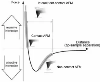
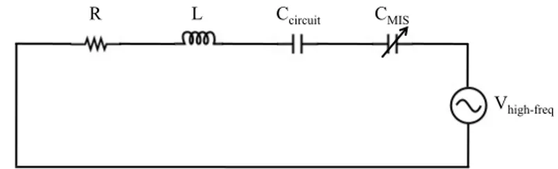
sam-ple. Various modes of operation of AFM are also indicated. . . . 29 2.2 Experimental set-up for Scanning Capacitance Microscopy . . . . 31 2.3 Schematic block diagram of resonating circuit used for ultra high
frequency capacitor sensor . . . 33 2.4 Schematic representation of (a) Conductive Atomic Force
Mi-croscopy, and (b) Torsion Resonance Conductive Atomic Force Microscopy applied to graphene. . . 34 2.5 (a) Optical microscopy of a few layers graphene sample, (b)
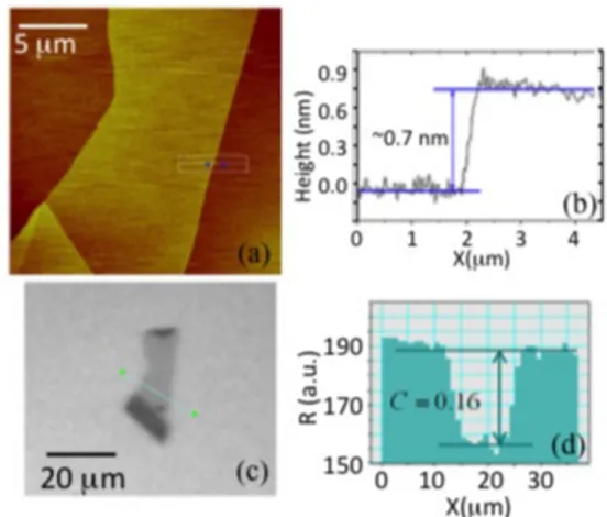
Mi-croRaman spectra measured on some selected positions indicated by the red, green and blue dots in the optical image, and (c) Atomic force microscopy image of the flake. . . 37 2.6 (a) AFM height map of the few layers graphene sample and (b)
height profile along the indicated line. . . 38 2.7 (a) Height of a few layers of graphene sheet versus the estimated
number of layers in the sheet. (b) Force-distance curves measured on FLG and (c) on SiO2. The black curves are collected with the tip approaching to the surface, while the red ones with the curves retracting from the surface. (d) Schematic explanation of the offset affecting the Step-height between single layers of graphene and SiO2. . . 39 2.8 (a) AFM image and (b) height linescan for a single layer graphene
flake deposited on 100 nm thick SiO2. (c) Optical microscopy on the same sample illuminated with light of 600 nm wavelength. (d) Illustration of the procedure to extract the optical contrast profile from the reflected light intensity. . . 41
LIST OF FIGURES
2.9 Optical contrast as a function of the flake thickness (and the number of graphene layers) for samples deposited on 300 nm SiO2 and illuminated with light of 400 nm (black triangles) and 600 nm (red squares) wavelengths. The lines represent the calculated contrast as a function of the number of layers. . . 41 2.10 MicroRaman spectra collected on several positions on the
epitax-ial graphene grown on 4H-SiC(0001) substrate. The spectrum collected on starting substrate (bare SiC) is also shown for com-parison. . . 43 2.11 Estimation of number of graphene layers by etching graphitized
SiC surface. The trenches are clearly seen in the phase images (a1), (b1) and (c1) (the scale bars are 5µm). The height profile taken over the etched regions on pristine 4H-SiC sample gives an estimation of overetched SiC. Progressively deeper trenches in (b) and (c) give an estimated 3, and 9 layers of graphene. . . 45 2.12 Fig. 3 High-resolution Transmission Electron Micrographs of
graphitized 4H-SiC(0001) (a) Sample 1, and (b) Sample 2. Graphene layers appear evident on SiC substrate. . . 45 2.13 Torsion Resonance Atomic Force Microscopy map in (a) and the
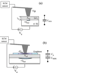
corresponding Torsion Resonance Conductive Atomic Force Mi-croscopy map in (b). In (c) are shown histograms extracted from the current map in (b). Evaluated three regions (region with graphene coverage (curves (ii) and (iii)) and region devoid of graphene (curve (i)) are indicated distinctly. . . 47 2.14 TR morphology (a) and current map (b) collected on EG2 sample. 48 3.1 Schematic illustration of the experimental system, when the AFM
tip is on SiO2 (a) and on graphene (b) . . . 58 3.2 Typical set of 25 |∆C|-Vg characteristics measured with the tip
at a fixed position on SiO2 (a) and at a fixed position on the graphene monolayer (b). In (c), set of 25 |∆C|-Vg characteris-tics measured on an array of 5 × 5 different tip positions in the region across the graphene monolayer and SiO2. The red and green curves are the calculated average values, respectively. In the inserts, the histograms of |∆C| at fixed bias (Vg=-8 V) is reported. . . 61
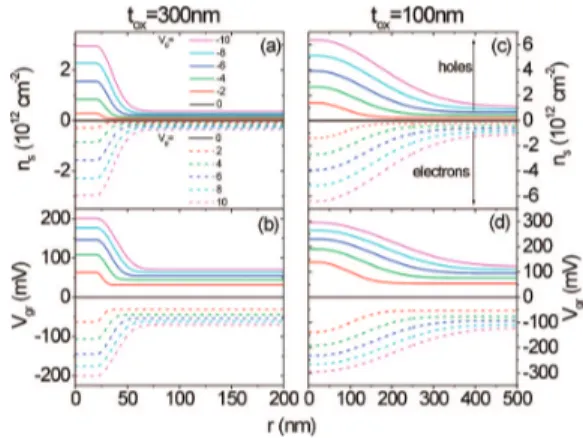
3.3 On the left axis, the average ratio N=|∆Ctot|/|∆CM OS| between the capacitance variations measured with the tip on graphene and with the tip on SiO2, for samples with 300 nm oxide thickness (a) and 100 nm oxide thickness (b). On the right axis, the average screening radius rs calculated from N(Vg) for the sample with 300 nm oxide thickness (a) and 100 nm oxide thickness (b). . . . 62 3.4 Screening charge density distribution for different values of the
applied bias Vg, for the sample with 300 nm oxide thickness (a) and 100 nm oxide thickness (c). Local potential on graphene Vgr(r) for different values of Vg, for the sample with 300 nm oxide thickness (b) and 100 nm oxide thickness (d). . . 65 3.5 Potential drop in graphene ∆Vgr (a), quantum capacitance Cq
(b), density of states DOS (c) versus Vg for the sample with 300 nm oxide thickness (black line) and 100 nm oxide thickness (red line). In (d) the minimum area ADOS necessary to accommodate the charge induced by the bias Vg, according to the density of states in graphene, is reported on the right scale, whereas the effective area determined form the data in Figure 3.3 is reported on the right scale. . . 67 3.6 The rs vs Vg curves for all the tip positions on graphene (a)
and, in the inset, the histogram of the rs values distribution for fixed Vg=-5 V. Similarly, in (b), the Cq vs Vg curves for all the tip positions and, in the inset, the histogram of the Cq values distribution for fixed Vg=-5 V are shown. Finally, in (c), the DOS vs Vg curves for all the tip positions and, in the inset, the histogram of the DOS values distribution for fixed Vg=-5 V are shown. . . 68 3.7 (a) Optical micrograph showing graphene deposited on STO.
Monolayer region can be seen with lighter contrast in a multi-layer stack. (b) Tapping mode AFM micrograph of a represen-tative DG-STO flake and (c) corresponding height profile in a linescan on monolayer-SrTiO3 region. . . 70 3.8 Representative characteristics obtained by Scanning Capacitance
Spectroscopy (SCapS) on (a) graphene deposited on SrTiO3 (DG-STO) and (b) graphene deposited on SiO2 (DG-SiO2). Two dis-tinct families of curves correspond to tip position ‘on graphene’ and ‘on substrate’ as indicated. A typical scan comprises of an array of 5×5 positions with an inter-step distance of 1μm×1μm. . 71
LIST OF FIGURES
3.9 Aef fas evaluated from the local capacitive measurements on DG-STO and DG-SiO2 as a function of EF is showed in (a). The corresponding Cq is depicted in (b). A relative increase in Cq of ~10× can be seen from the histograms in (c). . . 73 3.10 Local capacitance measurements (a) can be used to evaluate the
electron mean free path in graphene (b) supported by insulating and/or semiinsulating substrates. . . 75 4.1 Typical optical (a) and AFM (b) images on a sample containing
both monolayer (i) bilayer (ii) and multi-layer (iii) regions. The spots on the optical image indicate the spatial resolution of the Raman measurements. . . 81 4.2 Raman spectra on a single layer graphene not irradiated and
ir-radiated with 500 keV C ions at 1×10¹³, 2×10¹³, 5×10¹³ and 1×1014 cm−2 fluences. In the insert, the D peak for the four fluences is reported (here intensities are normalized). . . 83 4.3 AFM images acquired on 1×1 μm scan areas on SiO2 and
sup-ported graphene for not irradiated samples and for irradiated (fluences of 1×10¹³, 5×10¹³and 1×1014cm−2). Power spectra of the AFM maps were calculated for all the samples and reported in a–d. . . 86 4.4 Raman spectra taken after 1014 ion/cm2 irradiation in a single-,
double- and multi-layer graphene pieces together with the spec-trum of an as prepared single layer graphene . . . 87 4.5 Ratio of the D peak and G peak intensities (ID/IG) as a function
of the ion fluence for a single layer, a double layer and a multi-layer of graphene. . . 88 4.6 G’ peak for the irradiated (1013ions/cm2) single and double
lay-ers together with the signals obtained in the D line region, dupli-cated in frequency to compare them with the second order signal. 89 4.7 SCapS curves obtained on (a) pristine graphene, (b) graphene
irradiated with a fluence of 1×10¹³ ions/cm2, and (c) 1×10¹⁴ ions/cm2. . . 91 4.8 N (left axis) and Aef f (right axis) obtained on (a) pristine graphene,
and graphene irradiated with a fluence of (b) 1×10¹³ ions/cm2 and (c) 1×10¹⁴ions/cm2. . . 92
4.9 Histograms showing quantitative variations for (a) N, (b) Aef f and (c) νF. The cases for pristine graphene are depicted in (1), while (2) and(3) indicate the cases for graphene irradiated with a fluence of 1×1013cm−2 and 1×1014cm−2 respectively. The two distributions observed distinctly indicate probed sites that are defected and non-defected, especially, the broader distribution at lower values are associated with defected sites. . . 93 4.10 Density of states (left axis) and quantum capacitance per unit
area (right axis) obtained on (a) pristine graphene, (b) graphene irradiated with a fluence of 1×10¹³ions/cm2and (c) a fluence of 1×10¹⁴ ions/cm2. Distributions of DOS at fixed backgate bias (Vg=1 V) for (d) pristine graphene and graphene irradiated with fluences of (e) 1×10¹³ions/cm2and (f) 1×10¹⁴ions/cm2. . . 95 4.11 | !C | vs Vg measurements on arrays of several tip positions
on (a) not irradiated graphene, and on irradiated graphene at fluences (b) 1×10¹³, and (c) 1×1014 cm−2, respectively. Curves measured with the tip on SiO2 reported for comparison. His-tograms of the capacitance values at Vg=1 V for (d) not irradi-ated graphene, and irradiirradi-ated graphene at (e) 1×10¹³, and (f) 1×1014 cm−2. (g) Percentage of counts under peaks 1 and 2 in the distributions vs the irradiated fluence. . . 97 4.12 Local electron mean free path vs V1/2
g and n1/2for several tip po-sitions on (a) not irradiated graphene and on irradiated graphene at fluences (b) 1×10¹³, and (c) 1×1014cm−2. . . 98 4.13 Local mobility vs Vg and n for several tip positions on (a) not
irradiated graphene, and on irradiated graphene at fluences (b) 1×10¹³, and (c) 1×1014cm−2. Histograms of µ and l at V
g= 1 V on (d) not irradiated graphene and (e,f) on irradiated graphene with the two fluences. . . 100 5.1 Schematic representation of graphene/substrate interface for (a)
graphene grown epitaxially on 4H-SiC(0001) (EG), (b) graphene exfoliated and deposited on 4H-SiC(0001) (DG-SiC), and (c) graphene exfoliated and deposited on SiO2 (DG-SiO2). Commonly ob-served buffer layer between the last SiC bilayer and first graphene layer at the interface in EG is depicted in (a). Such buffer layer is absent in DG-SiC and DG-SiO2. . . 109
LIST OF FIGURES
5.2 (a) Current map of DG on 4H-SiC(0001) at tip voltage of 1 V. The tip positions on graphene and on 4H-SiC are shown. (b) Typical set of SCurS I-V characteristics. Two distinct families of curves are associated with the tip positions on graphene and on 4H-SiC are indicated. . . 110 5.3 MicroRaman spectra collected on several positions on the
epi-taxial graphene grown on 4H-SiC(0001) substrate along with the spectrum collected on starting substrate (bare SiC) is also shown for comparison. The number of graphene layers was found to vary rapidly at micrometer scale. The estimated number of layers are depicted on each spectrum. . . 111 5.4 (a) Topography and (b) corresponding current map of EG on
4H-SiC(0001). The tip positions on regions covered by EG and on regions devoid of EG are indicated. The corresponding I-V curves are reported in (c). . . 112 5.5 Histograms of SBHs evaluated for Pt/graphene/4H-SiC and
Pt/4H-SiC in the cases of (a) DG and (b) EG. . . 113 5.6 Band diagrams of graphene/4HSiC(0001) Schottky contact for
(a) DG-SiC(0001) and (b) EG-SiC(0001). In contrast to DG, due to presence of positively charged buffer layer, the EG film is negatively doped. . . 114 5.7 Tapping mode AFM micrograph of (a) a prototypical graphene
flake deposited on 4H-SiC(0001) and (b) graphene epitaxially grown on 4H-SiC(0001). Corresponding linescan on a mono-layer exfoliated graphene in (c) and TR-CAFM map on epitaxial graphene in (d). . . 116 5.8 A typical set of SCS curves obtained on (a) graphene deposited on
4H-SiC(0001), (b) graphene epitaxially grown on 4H-SiC(0001). Two families of curves corresponding to SCS signal (i) on graphene and (ii) on 4H-SiC(0001) can be distinguished. . . 118 5.9 Screening length as evaluated in DG and EG. Wider variations
in rsfor EG can be observed and are indicative of local variations in electrostatic properties in EG. . . 119 5.10 Local variations, as evaluated from screening length (rs), in
quan-tum capacitance (Cq) are shown in (a) and (b) while those in local density of states (LDOS) are shown in (c) and (d) for (i) DG and (ii) EG. . . 120
5.11 Representative characteristics obtained by SCapS on (a) graphene deposited on 4H-SiC(0001) (DG-SiC), (b) graphene epitaxially grown on 4H-SiC(0001) (EG-SiC), and (c) graphene deposited on SiO2 (DG-SiO2). Two distinct families of curves correspond to tip placement (i) “on graphene” and (ii) “on substrate” are indicated. A typical scan comprises of an array of 5×5 positions with an interstep distance of 1×1 μm2. . . 122 5.12 Evaluated electron mean-free path in graphene (lgr) for (i)
DG-SiC, (ii) EG-DG-SiC, and (iii) DG-SiO2 is depicted in (a). In (b) are depicted the corresponding histograms plotted at nV g-n0 = 1.5×1011 cm−2. An average increase of ~4× and ~1.5× can be seen in lgr for DG-SiC and EG-SiC, respectively, as compared to lgr for DG-SiO2. . . 124 5.13 A representative graph of prominent limiting contributions to
the room temperature electron mean free path in graphene eval-uated for the cases of (a) DG-SiC and (b) DG-SiO2: lSP P (red up-triangles) and lci(green circles). The lciis simulated by vary-ing the charged-impurity density Nci. The best match between leq_sim(black solid line) and lavg_exp(blue diamonds) was found for Nci= 7×1010cm−2 (DG-SiC), 1.8×1011 cm−2 (DG-SiO2). . . 126
List of Tables
5.1 The characteristic SPP frequencies and the corresponding Fröh-lich coupling constants for SiO2 and 4H-SiC. . . 126
Chapter 1
Introduction
1.1 Nanoscale science and technology: A primer
Nanoscale science and technology is forming and use of materials, structures, devices, and systems that have unique properties because of their small size as well as it includes the technologies that enable the control of materials at the nanoscale. National Nanotechnology Initiative (NNI) [1] defines Nanoscale sci-ence and technology as ‘the understanding and control of matter at dimensions of roughly 1 to 100 nm, where unique phenomena enable novel applications.’
What does it involve?
Current research in nanoscience and technology involves three main thrusts of research [2]:
• nanoscale science (or ‘nanoscience’ – the science of interaction and behav-ior at the nanoscale),
• nanomaterials development (the actual experimental development of nano-scale materials, including their use in device applications), and
• modeling (computer modeling of interactions and properties of nanoscale materials).
With nanoscience and technology, we start on the atomic scale and, controlling atomic/molecular placement and arrangement, we build up the technology into
unique devices, materials, and structures. This new type of formation requires new types of synthesis, requiring a new understanding of the formation of ma-terials on the nanoscale. Furthermore, many mama-terials have extremely unique properties when they are developed at a nanoscale. Many materials configure themselves in different atomic arrangements not seen in the bulk form of the same materials. Understanding the changes that these materials undergo as they are formed on a smaller scale is vital to developing the use of these materials in devices.
Nanoscale science and technology is a multidisciplinary field. Since, on the nanoscale, the laws of nature merge the laws of the very small (quantum me-chanics) and the laws of the large (classical physics), physics is very important to understanding nanotechnology; since the material is vital to the function of device and structure, the science and engineering of materials are vital to de-veloping nanotechnology. Additionally, specific applications require extensive knowledge from chemistry and biology as well.
Characterization tools
Nanoscale science and technology has been propelled further by the character-ization tools capable of ‘seeing at the nanoscale’ by enabling us to perceive further and deeper than we were able to before. Prominent amongst them are, • Electron microscopy: The development of electron microscopy has made possible imaging materials at the nanoscale. For a typical low-voltage scanning electron microscope (SEM) with a beam energy of 5 kiloelectron volts (keV), the wavelength of the electron beam is around 0.0173 nm. For a 100 keV transmission electron microscope (TEM), the wavelength is even smaller, 0.0037 nm. For a 400 keV electron beam, the wavelength is 0.00028 nm. Of course, this theoretical limit and the actual resolu-tion of the microscope are affected significantly by aberraresolu-tions, defects, astigmatisms, and other practical considerations to reduce the resolution [3]. However, with certain configurations, these electron microscopes can even distinguish individual atoms. This enables us to discover and inves-tigate nanomaterials and study how their atomic makeup impacts their properties.
• Scanning probe microscopy (SPM): It is not a ‘microscope’ in a conven-tional way [4]. In general, a scanning probe ‘feels’ the specimen and different aspects of it can be observed and understood by the acquired images. Scanning probe microscopes provide researchers with several new
Sushan t Sonde, PhD in Nanoscience, Scuola Sup eriore of the Univ ersit y of Catania, 2010 .
1.1. Nanoscale science and technology: A primer
directions in which to study a material or manipulate it. For one, they provide three-dimensional information about the surface of the specimen instead of the two-dimensional information that electron microscopes pro-vide. Samples viewed by some types of SPM do not require any special treatments that irreversibly alter the sample. Furthermore, it is easier to study macromolecules and biological samples with an SPM than it is with electron microscopes. Electron microscopes require a vacuum, while SPMs can typically be used in a standard room environment or even in liquid. Scanning probe microscopy does have its limits such as low throughput, probe tip wear, atmospheric disturbance. Despite this SPM based tech-niques are important for characterization and manipulation at nanoscale.
Nanomaterials
Current nanoscale science and technology has a heavy focus on the discovery, characterization, and utilization of nanomaterials. Formation of such materi-als can be done either by breaking to smaller fractions from larger, known as ‘top-down’ technology; or the formation of materials from atomic or molecular structures known as ‘bottom-up’ technology. The materials that are being de-veloped can be divided into two basic categories: organic (i.e., carbon based) and inorganic (i.e., not carbon based).
Carbon nanomaterials include,
• the buckyballs (all three spatial dimensions are confined to nanoscale – referred to as zero dimensional materials),
• carbon nanotubes (two spatial dimensions are confined to nanoscale – referred to as one dimensional materials) and very recently,
• graphene (one spatial dimension is confined to nanoscale – referred to as two dimensional materials).
The equivalent of these in inorganic materials are quantum dots (QDs), nanowires and ‘thin films’.
Considering that the topic of this thesis work is fabrication, identification and characterization of graphene for its use in prospective electronic applications, the next section traces current semiconductor technology’s path into nanoscale regime, and how this has led to the technology facing fundamental limitations. This to a greater extent has motivated pursuits for alternative technologies. The succeeding section reviews carbon materials in nanoelectronics; their relative
Sushan t Sonde, PhD in Nanos cience, Scuola Sup eriore of the Univ ersit y of Catania, 2010 .
advantages to incumbent technology and the research efforts that have been made to establish carbon materials into mainstream electron device applications.
1.2 Nanoelectronics in retrospect
The semiconductor sector is one of the highest tempo fields of the business in the world, whether in communications, in the automobile industry, in rela-tion to broadband and access technology, in mobile communicarela-tions, healthcare equipments or memory products [5]. With its unparallel technological successes semiconductor products have brought about a revolution in all strata of to-day’s modern life. Advances powered by semiconductors give businesses and consumers new flexibility, freedom, and opportunity. Activities that once con-fined people to the home or office can now be performed at any time any place, almost anywhere in the world. The semiconductor industry is bringing new opportunities, socio-economic advance and new human development to nations and societies around the world [6].
For the past four decades Silicon (Si) has been the flag-bearer of this mega industry–almost synonymous with it. Si, found in ordinary sand, is the second most abundant element in the earth’s crust after oxygen. With robust bandgap of 1.1 eV together with higher specific resistance resulting in far lower reverse current, Si surpassed other materials (especially Germanium, bandgap of 0.67 eV) as a material of choice to make transistors [?]. But the greatest asset of Si proved to be the fact that it readily sustains a protective oxide layer grown on its surface [7]. Frosh and Derick went on to demonstrate how this silicon dioxide (SiO2) coating could be used as a selective mask in the diffusion process [8] leading to its use for junction formation. The experience gained by fabrication of junctions via SiO2masking in bipolar devices led D. Kahng and M. M. Atalla to report the first MOSFET (Metal-Oxide-Semiconductor Field-Effect-Transistor) on a Si substrate in 1960 [9]. The observation of junction passivation by Hoerni in the planar process in 1960 led to its use for improved junction characteristics [10]. Using SiO2it was possible to construct planar semiconducting structures, each layer essentially separated by a thin oxide layer. SiO2 proved to be an extremely good insulator on which Al wiring could subsequently be adherently deposited [11]. This planar technology opened a new era in the semiconductor integration propelling the growth of Semiconductor industry by many-folds. Thus, Silicon’s superior behavior at high temperature and great versatility of its oxide surface layer in manufacturing processes led to its current dominance of the semiconductor industry.
Sushan t Sonde, PhD in Nanoscience, Scuola Sup eriore of the Univ ersit y of Catania, 2010 .
1.3. Carbon materials for prospective nanoelectronics
In 1965, Gordon Moore observed that the total number of devices on a chip would double every 12 months. He predicted that the trend would continue in the 1970’s but would slow down in the 1980s, when the total number of devices would double every 24 months. Known widely as ‘Moore’s law’, it became the guiding principle for the Semiconductor industry. These observations made the case for continued wafer and die size growth, defect density reduction and increased transistor density as manufacturing matured and technology scaled [12]. Throughout all this equally important has been the circuit cleverness, i.e. the reduction in number of devices and chip area to implement the given circuit or function. Hence, the driving force for continued integration complexity has been the reduction in cost per function for the chip [13]. The 1970’s brought on the widespread use of dimensional scaling as the predominant means to increase device density and lower transistor cost via R. Dennard’s scaling methodology [14].
Since then device scaling has been the engine driving the integrated circuit (IC) microelectronics revolution [15]. The critical elements in device scaling are the gate dielectric thickness, the channel length and the junction (and now) extension junction depth [16]. These dimensions have long reduced from their early 1970’s values of 50–100 nm, 7.5 μm and 1 μm respectively to 1.1–1.6 nm, 45 nm and 25 nm (extension junction depth) for the high performance microprocessor (MPU) for the 100 nm technology generation as described in ITRS [17]. Si technology has already entered the regime of nanotechnology (sub 100 nm) by roadmap driven feature size reduction. But as the device features are pushed towards the deep sub-100 nm regime, the conventional scaling methods of the semiconductor industry face increasing technological and fundamental challenges [18].
1.3 Carbon materials for prospective
nanoelec-tronics
The obstacles for Si circuitry has called for a need for development of alterative device technologies which are designed and interconnected in an appropriate architecture for nanoscale regime. This provides an opportunity to develop new concepts and/or new materials for the electronic applications. Though some paradigm shifting approaches involve development of spin-based devices, oth-ers continue to pursue traditional electron transport based devices, but involve replacement of the conducting channel in the FET with carbon nanomaterials
Sushan t Sonde, PhD in Nanos cience, Scuola Sup eriore of the Univ ersit y of Catania, 2010 .
such as one-dimensional (1D) carbon nanotubes (CNT) or two-dimensional (2D) graphene layers, which have superior electrical properties [19]. As an added pos-sibility the semiconducting CNTs, being a direct bandgap material, provide an ideal system to study optics and optoelectronics in one dimension and explore the possibility of basing both electronics and optoelectronic technologies on the same material.
From a device integration point of view metallic, particularly multiwalled, CNTs offer the possibility of use as high-performance interconnects in very-large-scale integrated systems [20], whereas semiconducting CNTs are useful candidates to be used as a basis of novel transistors. Indeed, the first CNT-FETs were reported in 1998 [21, 22]. The atomic and electronic structures of the CNT give it a number of unique advantages as a FET channel. First, its small diameter (1–2 nm) allows the gate to control the potential of the chan-nel optimally. The strong coupling with the gate makes the CNT the ultimate ‘thin-body’ semiconductor system and allows the devices to be made shorter while avoiding the short-channel effects [23], which basically involve the loss of control of the device by the gate field. The fact that all bonds in the CNT are satisfied and the surface is smooth also has important implications. Scattering by surface states and roughness, which affects conventional FETs, especially at high gate voltage values, is absent. The key advantage is the low scattering in the CNT and the high mobility of the FET channel.
For the use in logic applications CNTFETs offer multiple advantages over Si MOSFETs because of their much lower capacitance of the order of ~10 aF (for a dCN T (diameter of CNT) = 1 nm, L (lenght of CNT) = 10 nm, tox(gate oxide thickness) = 5 nm device) and their somewhat lower operating voltage. Furthermore, the small size of the CNTs allow the fabrication of aligned ar-rays with high packing density. Also CNTFETs have lower switching energy per logic transition. The dynamic switching energy of a device is given by: 1/2(Cdev+Cwire)V2, where Cdev and Cwire are the device and wiring capaci-tance contributions, respectively. To minimize the switching energy, minimum-sized devices, and interconnects should be used, as well as the minimum supply voltage. Then the CNT can have a considerable advantage, of up to a factor of six, because of its smaller intrinsic capacitance and size [24].
The fabrication and evaluation of CNT-based devices has advanced beyond single devices to include logic gates [25, 26, 27, 28] and, more recently more com-plex structures such as ring oscillators have been fabricated [29] using the energy efficient CMOS (complementary-MOS) architecture (by utilizing the ambipolar behavior of the undoped CNT).
In addition to be used as transistors, CNTFET devices can also be used as
Sushan t Sonde, PhD in Nanoscience, Scuola Sup eriore of the Univ ersit y of Catania, 2010 .
1.3. Carbon materials for prospective nanoelectronics
a light emitter or a light detector. Choosing between these different modes of operation only requires changes in the electrical inputs. In order to fabricate LEDs, or other electroluminescent devices, one must generate and bring together significant populations of electrons and holes. The quasi-1D character of the CNT confines the two types of carriers, which are driven towards each other. Indeed, radiative recombination in an ambipolar CNTFET was reported in ref. [30]. Although the mechanism of that emission is similar to that of an LED, there is an important difference: the CNT is not doped so there is no clear p–n junction. As a result, the light does not originate from a fixed point along the CNT, but its origin can be translated by simply changing the gate voltage, which determines the local potential in a long CNT device [30]. Single CNT photoconductivity was reported for the first time in 2003 [31, 32]. The resonant excitation of a CNT generates an electric current and can be used as a nanosized photodetector, a photo switch, or as a spectroscopic tool. Alternatively, in the open-circuit configuration the device generates a photovoltage.
Opportunities also exist for integrating nanotube electronics with other chem-ical, mechanchem-ical, or biological systems. For example, nanotube electronic de-vices function perfectly well under biological conditions (i.e., salty water) and have dimensions comparable to typical biomolecules (e.g., DNA, whose width is approximately 2 nm). This makes them an excellent candidate for electrical sensing of individual biomolecules. There are also a host of other device geome-tries beyond the simple wire and FET structures that are under exploration, for example the p-n and p-n-p devices [33] and [34], nanotube/nanotube junctions [35, 36, 37], and electromechanical devices [38, 39].
However the major challenge faced by CNT based technology is the device manufacturability. Although a great deal of work has been done, the progress to date has been modest [40]. For example, in tube synthesis, the diameter of the tubes can be controlled, but not the chirality. As a result, the tubes are a mix-ture of metal and semiconductors. In chemical vapor deposition (CVD) growth of CNT, the general location for tube growth can be controlled by patterning the catalyst material, but the number of tubes and their orientation relative to the substrate are still not well defined. Furthermore, the high growth tem-perature (900 °C) for CVD tubes is incompatible with many other standard Si processes. The alternative approach, depositing tubes on a substrate after growth, avoids this high temperature issue but suffers from the chirality and positioning limitations. In addition to the patterning and device architecture related challenges CNT based devices possess unacceptably large contact resis-tance. To date, there are no reliable, rapid, and reproducible approaches to creating complex arrays of nanotube devices. This manufacturing issue is by far
Sushan t Sonde, PhD in Nanos cience, Scuola Sup eriore of the Univ ersit y of Catania, 2010 .
the most significant impediment to using nanotubes in electronics applications. However, the problems faced by CNT based electronics can be obviated while retaining their essential electronic properties by using the fundamental building block of both a graphite crystal and a CNT – the graphene layer.
1.4 Graphene
A two-dimensional (2D) allotrope of carbon is called graphene. It is made out of carbon atoms arranged on a honeycomb structure made out of hexagons. Graphene assumes an important role in understanding the electronic properties of all other carbon allotropes. As evidence, Fullerenes [41] are molecules where carbon atoms are arranged spherically, and hence, from the physical point of view, are zero-dimensional objects with discrete energy states. Fullerenes can be obtained from graphene with the introduction of pentagons (that create positive curvature defects), and hence, fullerenes can be thought as wrapped-up graphene. Carbon nanotubes [42, 43] are obtained by rolling graphene along a given direction and reconnecting the carbon bonds. Hence carbon nanotubes have only hexagons and can be thought of as one-dimensional (1D) objects. Graphite is a three dimensional (3D) allotrope of carbon.
Graphene layer is shown schematically in Figure 1.1(a). The atomic struc-ture is characterized by two types of C–C bonds (σ", π) constructed from the four valence orbitals (2s, 2px, 2py, 2pz), where the z-direction is perpendicular to the sheet [44]. Three σ"-bonds join a C atom to its three neighbors. They are quite strong, leading to optical-phonon frequencies much higher than ob-served in diamond. In addition, the C–C bonding is enhanced by a fourth bond associated with the overlap of pz (or π) orbitals. The electronic properties of graphene, graphite and carbon nanotubes are determined by the bonding π-and antibonding π*-orbitals, that form wide electronic valence π-and conduction bands (Figure 1.1(b)).
Theoretical calculations show that the π-band overlap in graphite disappears as the layers are further separated over their equilibrium distance in graphite. This leads to decoupled graphene layers that can be described as a zero-gap semiconductor. The π-band electronic dispersion for graphene near the six cor-ners of the 2D hexagonal Brillouin zone is found to be linear. Thus, ‘cones’ of carriers (holes and electrons) appear in the corners of a 2D Brillouin zone whose points touch at the Fermi energy, as shown in Figure 1.1(c). The linear electronic band dispersion leads to the description of carriers in graphene as ‘massless Dirac fermions’. The six points where the cones touch are referred to
Sushan t Sonde, PhD in Nanoscience, Scuola Sup eriore of the Univ ersit y of Catania, 2010 .
1.5. Graphene and other 2D Semiconductor structures
Electron and Phonon Properties of Graphene 675
Fig. 1. Illustration of the carbon valence orbitals. (a) The three inplane σ (s, px, py)
orbitals in graphene and the π (pz) orbital perpendicular to the sheet. The inplane
σ and the π bonds in the carbon hexagonal network strongly connect the carbon
atoms and are responsible for the large binding energy and the elastic properties of the graphene sheet. The π orbitals are perpendicular to the surface of the sheet. The corresponding bonding and the antibonding σ bands are separated by a large energy gap of∼ 12 eV (b), while the bonding and antibonding π states lie in the
vicinity of the Fermi level (EF). Consequently, the σ bonds are frequently neglected
for the prediction of the electronic properties of graphene around the Fermi energy. Dirac cones located at the six corners of the 2D Brillouin zone are illustrated in (c)
the optical phonons in graphene that are directly accessible by Raman spec-troscopy and give rise to the most prominent Raman peaks when graphene is folded into nanotubes. We focus on their coupling to electrons, which is key to understanding many phenomena in graphene and nanotubes.
For example, it was recently argued that in doped graphene, the adia-batic Born–Oppenheimer approximation [16], valid in many solid-state sys-tems, breaks down [17]. The electron–phonon interaction in graphene has also been carefully re-examined and has been recently shown to give rise to Kohn anomalies in the phonon dispersion at important points (Γ , K) in the Brillouin zone where the phonons can be studied by Raman spectroscopy [18–
21]. Many of these new ideas proposed for graphene and nGLs carry over to nanotubes. Kohn anomalies are responsible for the different Raman spectra of metallic and semiconducting nanotubes, and non-Born–Oppenheimer effects strongly shape the Raman spectra of doped and annealed nanotubes [19,22]. These connections are also discussed in this review.
2 Electronic Properties and Transport Measurements
2.1 Graphene
2.1.1 Electronic Band Structure
Figure 1.1: Illustration of the carbon valence orbitals. (a) The three inplane σ" (s, px , py ) orbitals in graphene and the π (pz) orbital perpendicular to the sheet. The inplane σ" and the π bonds in the carbon hexagonal network strongly connect the carbon atoms and are responsible for the large binding energy and the elastic properties of the graphene sheet. The π orbitals are perpendicular to the surface of the sheet. The corresponding bonding and the antibonding σ" bands are separated by a large energy gap of ~12 eV (b), while the bonding and antibonding π states lie in the vicinity of the Fermi level (EF). Consequently, the σ"bonds are frequently neglected for the prediction of the electronic properties of graphene around the Fermi energy. Dirac cones located at the six corners of the 2D Brillouin zone are illustrated in (c) (adopted from [44]).
as the ‘Dirac’ points.
1.5 Graphene and other 2D Semiconductor
struc-tures
Graphene is a true two-dimensional electron system. There are, broadly speak-ing, four qualitative differences [45] between 2D graphene and 2D semiconductor systems found in Si inversion layers in MOSFETs, GaAs-AlGaAs heterostruc-tures, quantum wells, etc.
1. First, 2D semiconductor systems typically have very large (>1 eV) bandgaps so that 2D electrons and 2D holes must be studied using completely dif-ferent electron-doped or hole-doped structures. By contrast, graphene is a gapless semiconductor with the nature of the carrier system changing at the Dirac point from electrons to holes (or vice versa) in a single structure. A direct corollary of this gapless (or small gap) nature of graphene, is of course, the ‘always metallic’ nature of 2D graphene, where the chemical
Sushan t Sonde, PhD in Nanos cience, Scuola Sup eriore of the Univ ersit y of Catania, 2010 .
potential (‘Fermi level’) is always in the conduction or the valence band. By contrast, the 2D semiconductor becomes insulating below a threshold voltage, as the Fermi level enters the bandgap.
2. Graphene systems are chiral, whereas 2D semiconductors are non-chiral. Chirality of graphene leads to some important consequences for transport behavior. (For example, 2kF -backscattering is suppressed in MLG at low temperature.)
3. Monolayer graphene dispersion is linear, whereas 2D semiconductors have quadratic energy dispersion. This leads to substantial quantitative differ-ences in the transport properties of the two systems.
4. Finally, the carrier confinement in 2D graphene is ideally two-dimensional, since the graphene layer is precisely one atomic monolayer thick. For 2D semiconductor structures, the quantum dynamics is two dimensional by virtue of confinement induced by an external electric field, and as such, 2D semiconductors are quasi-2D systems, and always have an average width or thickness 〈t〉 (≈ 5 nm to 50 nm) in the third direction with 〈t〉≤ λF, where λF is the 2D Fermi wavelength (or equivalently the carrier de Broglie wavelength). The condition 〈t〉 < λF defines a 2D electron system. In particular, for a system to be defined as 2D, λF = 2π/kF > t where λF is the Fermi wavelength (i.e. the operational quantum wavelength of the system). For graphene, we have λF ≈ (35/√n") nm, where n" = n/(1012 cm−2), and since t ≈ 0.1 nm to 0.2 nm (the monolayer atomic thickness), the condition λF>>t is always satisfied, even for unphysically large n=1014 cm−2. The clas-sic technique to verify the 2D nature of a particular system is to show that the orbital electronic dynamics is sensitive only to a magnetic field perpendicular to the 2D plane (or more precisely, that the system response depends only on the perpendicular component Bcosθ of an applied magnetic field (B) at angle θ to the z-direction) of confinement. Therefore, the observation of magnetoresis-tance oscillations (Shubnikov-de Hass effect) depending only on Bcosθ, proves the 2D nature, or if the cyclotron resonance properties depend only on Bcosθ, then the 2D nature is established. Both of these are true in graphene. The most definitive evidence for 2D nature, however, is the observation of the quantum Hall effect, which is a quintessentially 2D phenomenon. Any system manifest-ing an unambiguous quantized Hall plateau is 2D in nature, and therefore the observation of the quantum Hall effect in graphene in 2005 by Novoselov et al. [46, 47] and Zhang et al. is an absolute evidence of its 2D nature (Figure 1.2).
Sushan t Sonde, PhD in Nanoscience, Scuola Sup eriore of the Univ ersit y of Catania, 2010 .
1.5. Graphene and other 2D Semiconductor structures
PROGRESS ARTICLE
nature materials| VOL 6 | MARCH 2007 | www.nature.com/naturematerials 187
phase
9,10,57. Th e additional phase leads to a π-shift in the phase of
quantum oscillations and, in the QHE limit, to a half-step shift .
Bilayer graphene exhibits an equally anomalous QHE (Fig 4b)
56.
Experimentally, it shows up less spectacularly. Th e standard sequence
of Hall plateaux σ
xy= ±N4e
2/h is measured, but the very fi rst plateau
at N = 0 is missing, which also implies that bilayer graphene remains
metallic at the neutrality point
56. Th e origin of this anomaly lies in the
rather bizarre nature of quasiparticles in bilayer graphene, which are
described
58by
ћ
22m
–
=
H
(k
0
0
x+ik
y)
2(k
x–ik
y)
2.
(2)
Th is hamiltonian combines the off -diagonal structure, similar to the
Dirac equation, with Schrödinger-like terms p
ˆ
2/2m. Th e resulting
quasiparticles are chiral, similar to massless Dirac fermions, but have
a fi nite mass m ≈ 0.05m
0. Such massive chiral particles would be an
oxymoron in relativistic quantum theory. Th e Landau quantization
of ‘massive Dirac fermions’ is given
58by E
N
= ± ħω
√N(N–1) with two
degenerate levels N = 0 and 1 at zero E (ω is the cyclotron frequency).
Th is additional degeneracy leads to the missing zero-E plateau
and the double-height step in Fig. 4b. Th ere is also a pseudospin
associated with massive Dirac fermions, and its orbital rotation
leads to a geometrical phase of 2π. Th is phase is indistinguishable
from zero in the quasiclassical limit (N >> 1) but reveals itself in the
double degeneracy of the zero-E LL (Fig. 4d)
56.
It is interesting that the ‘standard’ QHE with all the plateaux
present can be recovered in bilayer graphene by the electric
fi eld eff ect (Fig. 4b). Indeed, gate voltage not only changes n but
simultaneously induces an asymmetry between the two graphene
layers, which results in a semiconducting gap
59,60. Th e electric-fi
eld-induced gap eliminates the additional degeneracy of the zero-E LL
and leads to the uninterrupted QHE sequence by splitting the double
step into two (Fig. 4e)
59,60. However, to observe this splitting in the
QHE measurements, the neutrality region needs to be probed at
fi nite gate voltages, which can be achieved by additional chemical
doping
60. Note that bilayer graphene is the only known material in
which the electronic band structure changes signifi cantly via the
electric fi eld eff ect, and the semiconducting gap ∆E can be tuned
continuously from zero to ≈0.3 eV if SiO
2is used as a dielectric.
CONDUCTIVITY ‘WITHOUT’ CHARGE CARRIERS
Another important observation is that graphene’s zero-fi eld
conductivity σ does not disappear in the limit of vanishing n but
instead exhibits values close to the conductivity quantum e
2/h per
carrier type
9. Figure 5 shows the lowest conductivity σ
min
measured
near the neutrality point for nearly 50 single-layer devices. For
all other known materials, such a low conductivity unavoidably
leads to a metal–insulator transition at low T but no sign of the
transition has been observed in graphene down to liquid-helium T.
Moreover, although it is the persistence of the metallic state with σ
of the order of e
2/h that is most exceptional and counterintuitive,
a relatively small spread of the observed conductivity values
(see Fig. 5) also allows speculation about the quantization of
σ
min. We emphasize that it is the resistivity (conductivity) that is
quantized in graphene, in contrast to the resistance (conductance)
quantization known in many other transport phenomena.
Minimum quantum conductivity has been predicted for Dirac
fermions by a number of theories
5,45,46,48,61–65. Some of them rely on
a vanishing density of states at zero E for the linear 2D spectrum.
However, comparison between the experimental behaviour of
massless and massive Dirac fermions in graphene and its bilayer
allows chirality- and masslessness-related eff ects to be distinguished.
To this end, bilayer graphene also exhibits a minimum conductivity of
the order of e
2/h per carrier type
56,66, which indicates that it is chirality,
rather than the linear spectrum, that is more important. Most theories
suggest σ
min= 4e
2/hπ, which is about π times smaller than the typical
values observed experimentally. It can be seen in Fig. 5 that the
experimental data do not approach this theoretical value and mostly
cluster around σ
min= 4e
2/h (except for one low-μ sample that is rather
unusual by also exhibiting 100%-normal weak localization behaviour
at high n; see below). Th is disagreement has become known as ‘the
mystery of a missing pie’, and it remains unclear whether it is due
2 0 6 4 0 4 2 Undoped Doped 10 4 K 12 T 4 K 14 T 5 0 –4 –2 0 ½ –½ n (1012 cm–2) –100 –50 50 100 –8 –6 –4 –2 Vg (V) ρxx (kΩ ) a b c d e D 0 E E E –32 2 3 –52 2 5 –72 2 7 σxy (4e 2/h ) σ xy (4e 2 /h )
Figure 4 Chiral quantum Hall effects. a, The hallmark of massless Dirac fermions is QHE plateaux in σxy at half integers of 4e2/h (adapted from ref. 9). b, Anomalous QHE for massive Dirac fermions in bilayer graphene is more subtle (red curve56): σ
xy exhibits the standard QHE sequence with plateaux at all integer N of 4e2/h except for N = 0. The missing plateau is indicated by the red arrow. The zero-N plateau can be recovered after chemical doping, which shifts the neutrality point to high Vg so that an asymmetry gap (≈0.1eV in this case) is opened by the electric fi eld effect (green curve60). c–e, Different types of Landau quantization in graphene. The sequence of Landau levels in the density of states D is described by EN∝ √N for massless Dirac fermions in single-layer graphene (c) and by EN∝ √N(N–1) for massive Dirac fermions in bilayer graphene (d). The standard LL sequence EN∝ N + ! is expected to recover if an electronic gap is opened in the bilayer (e).
Figure 1.2: Quantum Hall effect in graphene. The plataue in σxyat half integers of 4e2/! is a hallmark of massless Dirac fermions. ρ
xx vanishes for the same carrier concentrations.
In fact, the quantum Hall effect in graphene persists to room temperature [48], indicating that graphene remains a strict 2D electronic material even at room temperature.
As a final note, from a structural viewpoint the existence of finite 2D flakes of graphene with crystalline order at finite temperature does not in any way violate the Hohenberg-Mermin-Wagner-Coleman theorem, which rules out the breaking of a continuous symmetry in two dimensions. This is because the theorem only asserts a slow power law decay of the crystalline (i.e. positional order) correlation with distance, and hence, very large flat 2D crystalline flakes of graphene (or for that matter, of any material) are manifestly allowed by this theorem. Hence, it is not forbidden to have finite 2D crystals with quasi-long-range positional order at finite temperatures, which is what we have in 2D graphene flakes [45]. Sushan t Sonde, PhD in Nanos cience, Scuola Sup eriore of the Univ ersit y of Catania, 2010 . 11
trino” billiards
!
Berry and Modragon, 1987
;
Miao et al.,
2007
". It has also been suggested that Coulomb
interac-tions are considerably enhanced in smaller geometries,
such as graphene quantum dots
!
Milton Pereira et al.,
2007
", leading to unusual Coulomb blockade effects
!
Geim and Novoselov, 2007
" and perhaps to magnetic
phenomena such as the Kondo effect. The transport
properties of graphene allow for their use in a plethora
of applications ranging from single molecule detection
!
Schedin et al., 2007
;
Wehling et al., 2008
" to spin
injec-tion
!
Cho et al., 2007
;
Hill et al., 2007
;
Ohishi et al., 2007
;
Tombros et al., 2007
".
Because of its unusual structural and electronic
flex-ibility, graphene can be tailored chemically and/or
struc-turally in many different ways: deposition of metal
at-oms
!
Calandra and Mauri, 2007
;
Uchoa et al., 2008
" or
molecules
!
Schedin et al., 2007
;
Leenaerts et al., 2008
;
Wehling et al., 2008
" on top; intercalation #as done in
graphite intercalated compounds
!
Dresselhaus et al.,
1983
;
Tanuma and Kamimura, 1985
;
Dresselhaus and
Dresselhaus, 2002
"$; incorporation of nitrogen and/or
boron in its structure
!
Martins et al., 2007
;
Peres,
Klironomos, Tsai, et al., 2007
" #in analogy with what has
been done in nanotubes
!
Stephan et al., 1994
"$; and using
different substrates that modify the electronic structure
!
Calizo et al., 2007
;
Giovannetti et al., 2007
;
Varchon et
al.
, 2007
;
Zhou et al., 2007
;
Das et al., 2008
;
Faugeras et
al.
, 2008
". The control of graphene properties can be
extended in new directions allowing for the creation of
graphene-based systems with magnetic and
supercon-ducting properties
!
Uchoa and Castro Neto, 2007
" that
are unique in their 2D properties. Although the
graphene field is still in its infancy, the scientific and
technological possibilities of this new material seem to
be unlimited. The understanding and control of this
ma-terial’s properties can open doors for a new frontier in
electronics. As the current status of the experiment and
potential applications have recently been reviewed
!
Geim and Novoselov, 2007
", in this paper we
concen-trate on the theory and more technical aspects of
elec-tronic properties with this exciting new material.
II. ELEMENTARY ELECTRONIC PROPERTIES OF
GRAPHENE
A. Single layer: Tight-binding approach
Graphene is made out of carbon atoms arranged in
hexagonal structure, as shown in Fig.
2
. The structure
can be seen as a triangular lattice with a basis of two
atoms per unit cell. The lattice vectors can be written as
a
1=
a
2
!3,
%
3", a
2=
a
2
!3,−
%
3",
!1"
where a
&1.42 Å is the carbon-carbon distance. The
reciprocal-lattice vectors are given by
b
1=
2
!
3a
!1,
%
3", b
2=
2
!
3a
!1,−
%
3".
!2"
Of particular importance for the physics of graphene are
the two points K and K
!
at the corners of the graphene
Brillouin zone
!BZ". These are named Dirac points for
reasons that will become clear later. Their positions in
momentum space are given by
K =
'
2
!
3a
,
2
!
3
%
3a
(
, K
!
=
'
2
!
3a
,−
2
!
3
%
3a
(
.
!3"
The three nearest-neighbor vectors in real space are
given by
!
1=
a
2
!1,
%
3
"
!
2=
a
2
!1,−
%
3
"
"
3= − a
!1,0"
!4"
while the six second-nearest neighbors are located at
"
1!
= ±a
1,
"
2!
= ±a
2,
"
3!
= ±
!a
2−a
1".
The tight-binding Hamiltonian for electrons in
graphene considering that electrons can hop to both
nearest- and next-nearest-neighbor atoms has the form
!we use units such that #=1"
H
= − t
)
*i,j+,$!a
$,i †b
$,j+ H.c.
"
− t
!
)
**i,j++,$!a
$,i †a
$,j+ b
$,i†b
$,j+ H.c.",
!5"
where a
i,$!a
i†,$" annihilates !creates" an electron with
spin
$
!
$
= ↑ , ↓" on site R
ion sublattice A
!an
equiva-lent definition is used for sublattice B", t!&2.8 eV" is the
nearest-neighbor hopping energy
!hopping between
dif-ferent sublattices
", and t
!
is the next nearest-neighbor
hopping energy
1!hopping in the same sublattice". The
energy bands derived from this Hamiltonian have the
form
!
Wallace, 1947
"
E
±!k" = ± t
%
3 + f!k" − t
!
f
!k",
1
The value of t
!
is not well known but ab initio calculations
!
Reich et al., 2002
" find 0.02t%t
!
%
0.2t depending on the
tight-binding parametrization. These calculations also include the
effect of a third-nearest-neighbors hopping, which has a value
of around 0.07 eV. A tight-binding fit to cyclotron resonance
experiments
!
Deacon et al., 2007
" finds t
!
&0.1 eV.
a a 1 2 b b 1 2 K Γ k k x y 1 2 3 M δ δ δ A B K’
FIG. 2.
!Color online" Honeycomb lattice and its Brillouin
zone. Left: lattice structure of graphene, made out of two
in-terpenetrating triangular lattices
!a
1and a
2are the lattice unit
vectors, and
"
i, i=1,2,3 are the nearest-neighbor vectors
".
Right: corresponding Brillouin zone. The Dirac cones are
lo-cated at the K and K
!
points.
Figure 1.3: Honeycomb lattice and the Brillouin zone in graphene. (a) the lattice structure in graphene is made of two interpenetrating triangular lattices (a1and a2 are the lattice unit vectors and δi, i=1, 2, 3 are the nearest-neighbor vectors, (b) corresponding Brillouin zone. The Dirac cones are located at the K and K!
points (adopted from [49]).
1.6 Bandstructure of graphene and elementary
electronic properties [49]
Graphene honeycomb lattice along with its Brillouin zone is as shown in Figure 1.3.
The structure can be seen as a triangular lattice with a basis of two atoms per unit cell. The lattice vectors can be written as,
a1= a 2(3, √ 3) a2= a 2(3,− √ 3) (1.1)
where a≈1.42 Å is the carbon-carbon distance. The reciprocal-lattice vectors are given by,
b1= 2π 3a(1, √ 3) b2= 2π 3a(1,− √ 3) (1.2)
Of particular importance for the physics of graphene are the two points K and K!
at the corners of the graphene Brillouin zone (BZ). These are named Dirac points. Their positions in momentum space are given by,
K = !2π 3a, 2π 3√3a " K"= !2π 3a,− 2π 3√3a " (1.3) The three nearest-neighbor vectors in real space are given by,
12 Sushan t Sonde, PhD in Nanoscience, Scuola Sup eriore of the Univ ersit y of Catania, 2010 .
1.6. Bandstructure of graphene and elementary electronic properties δ1= a 2 # 1,√3$, δ2= a 2 # 1,−√3$, δ3=−a (1, 0) (1.4) while the six second-nearest neighbors are located at,
δ!1=±a1 δ
!
2=±a1 δ
!
3=±(a2− a1)
The tight-binding Hamiltonian for electrons in graphene considering that electrons can hop to both nearest-and next-nearest-neighbor atoms has the form (using units such that !=1)
H =−t% &a∗σ,ibσ,j+ h.c'− t% &a∗σ,iaσ,j+ b∗σ,ibσ,j+ h.c' (1.5) where ai,σ (a*i,σ) annihilates (creates) an electron with spin σ (σ=up, down) on site Ri on sublattice A (an equivalent definition is used for sublattice B), t (≈2.8 eV) is the nearest-neighbor hopping energy (hopping between different sublattices), and t!
is the next nearest-neighbor hopping energy (hopping in the same sublattice). The energy bands derived from this Hamiltonian have the form: E±(k) =±t(3 + f (k)− t!f (k) (1.6) f (k) = 2 cos#√3kya $ + 4 cos ) √ 3 2 kya * cos !3 2kxa "
where the plus sign applies to the upper (π) and the minus sign the lower (π*) band. It is clear from Equation 1.6 that the spectrum is symmetric around zero energy if t!
=0. For finite values of t!
the electron-hole symmetry is broken and the π and π* bands become asymmetric. Figure 1.4, shows the full band structure of graphene with both t and t’. The band structure close to one of the Dirac points (at the K or K’ point in the BZ) can be obtained by expanding the full band structure, Equation 1.6, close to the K (or K’) vector, Equation 1.3, as k = K + q, with |q|<<K: [50], E±(q)≈ ±νF|q| + O !#q K $2" (1.7) where q is the momentum measured relatively to the Dirac points and νF is the Fermi velocity, given by νF = 3ta/2, with a value νF ≈1×10⁶m/s.
Sushan t Sonde, PhD in Nanos cience, Scuola Sup eriore of the Univ ersit y of Catania, 2010 .
![Fig. 2. (a) Electronic band structure of graphene from ab-initio calculations [ 23 ]. The bonding σ and the antibonding σ ∗ bands are separated by a large energy gap](https://thumb-eu.123doks.com/thumbv2/123dokorg/4515797.34726/34.748.209.589.319.574/electronic-structure-graphene-calculations-bonding-antibonding-separated-energy.webp)